EP4016843A1 - Circuit de mise en forme de signal et circuit d'attaque de grille correspondant - Google Patents
Circuit de mise en forme de signal et circuit d'attaque de grille correspondant Download PDFInfo
- Publication number
- EP4016843A1 EP4016843A1 EP20896816.4A EP20896816A EP4016843A1 EP 4016843 A1 EP4016843 A1 EP 4016843A1 EP 20896816 A EP20896816 A EP 20896816A EP 4016843 A1 EP4016843 A1 EP 4016843A1
- Authority
- EP
- European Patent Office
- Prior art keywords
- nmos transistor
- gate
- resistor
- drain
- pmos transistor
- Prior art date
- Legal status (The legal status is an assumption and is not a legal conclusion. Google has not performed a legal analysis and makes no representation as to the accuracy of the status listed.)
- Granted
Links
Images


Classifications
-
- H—ELECTRICITY
- H03—ELECTRONIC CIRCUITRY
- H03K—PULSE TECHNIQUE
- H03K5/00—Manipulating of pulses not covered by one of the other main groups of this subclass
- H03K5/01—Shaping pulses
-
- H—ELECTRICITY
- H03—ELECTRONIC CIRCUITRY
- H03K—PULSE TECHNIQUE
- H03K5/00—Manipulating of pulses not covered by one of the other main groups of this subclass
- H03K5/15—Arrangements in which pulses are delivered at different times at several outputs, i.e. pulse distributors
- H03K5/151—Arrangements in which pulses are delivered at different times at several outputs, i.e. pulse distributors with two complementary outputs
- H03K5/1515—Arrangements in which pulses are delivered at different times at several outputs, i.e. pulse distributors with two complementary outputs non-overlapping
-
- H—ELECTRICITY
- H03—ELECTRONIC CIRCUITRY
- H03K—PULSE TECHNIQUE
- H03K5/00—Manipulating of pulses not covered by one of the other main groups of this subclass
- H03K5/125—Discriminating pulses
- H03K5/1252—Suppression or limitation of noise or interference
-
- H—ELECTRICITY
- H03—ELECTRONIC CIRCUITRY
- H03K—PULSE TECHNIQUE
- H03K19/00—Logic circuits, i.e. having at least two inputs acting on one output; Inverting circuits
- H03K19/0175—Coupling arrangements; Interface arrangements
- H03K19/0185—Coupling arrangements; Interface arrangements using field effect transistors only
- H03K19/018507—Interface arrangements
- H03K19/018521—Interface arrangements of complementary type, e.g. CMOS
Definitions
- the present disclosure relates to the field of electricity, and in particular, to the field of circuit anti-interference technologies, and specifically refers to a signal shaping circuit and a corresponding gate driving circuit.
- offset noise In some control circuits, due to the deviation of an actual manufacturing process, there is a mismatch between two level shift circuits, and noise caused by an amplitude difference in output signals of the level shift circuits is called offset noise here.
- the offset noise may also be transmitted as an input signal by a subsequent-stage circuit, which may lead to a system failure due to an error state. In a traditional circuit structure, the difference signal cannot be identified and eliminated.
- control circuits in the form of integrated circuits have gradually replaced conventional control systems built by separate devices.
- High-voltage and low-voltage control circuits, various devices with protection functions, high-voltage power devices and other devices are integrated through packaging integration or process integration, to greatly improve the integration and reliability of the whole system.
- a half-bridge driving circuit which is mainly used to drive a power transistor of an external half-bridge topology.
- a bootstrap capacitive structure is more convenient and more widely used.
- an electrical signal of a high-voltage-side control circuit is mainly generated by dual short pulse circuits, and then on/off pulses are converted into normal control signals for a power transistor through an RS flip-flop.
- the high-voltage-side circuit uses a floating power supply, during fast switching, in a process of charging and discharging a parasitic capacitor, a displacement current is generated in a high-voltage level conversion circuit, and a voltage drop is formed on a resistor of a high-voltage side, that is, common mode noise.
- the voltage signal easily triggers a subsequent-stage circuit, leading to circuit damage or burnout due to an error state.
- a pulse filter circuit is used to eliminate the noise.
- Fairchild Semiconductor generally uses an analog filter circuit to filter out noise signals, and other companies such as Mitsubishi use digital filters to filter out noise.
- Fig. 1 shows an anti-noise high-side driving circuit in the related art, which includes a double-pulse generating circuit, a noise filter circuit, an RS flip-flop, and an output driving circuit.
- Fig. 2 is a circuit diagram of the noise filter circuit in the anti-noise high-side driving circuit in Fig. 1 .
- the objective of the present disclosure is to overcome at least one of the above-mentioned shortcomings of the related art, and provide a signal shaping circuit with good anti-interference effect and stable performance and a corresponding gate driving circuit.
- the signal shaping circuit and the corresponding gate driving circuit of the present disclosure are as follows:
- the signal shaping circuit includes a turn-on signal shaping module and a turn-off signal shaping module,
- the turn-on signal shaping module further includes a third PMOS transistor, a fifth NMOS transistor, a sixth NMOS transistor, and a fifth resistor;
- a gate driving circuit with the signal shaping circuit is provided, where the gate driving circuit further includes:
- the level shift circuit includes a ninth NMOS transistor and a tenth NMOS transistor,
- the level shift circuit further includes a first Zener diode and a second Zener diode;
- the noise filter circuit includes a first inverter chain, a ninth resistor, a third capacitor, a first Schmitt trigger, a second inverter chain, a tenth resistor, a fourth capacitor, and a second Schmitt trigger;
- the output stage driving circuit includes a first NAND gate, a third inverter chain, a fifth PMOS transistor, an eleventh resistor, a second NAND gate, a fourth inverter chain, an eleventh NMOS transistor, and a twelfth resistor;
- the output stage driving circuit includes a third NAND gate, a fourth NAND gate, a fifth inverter chain, a sixth inverter chain, a twelfth NMOS transistor, a thirteenth NMOS transistor, and a fourteenth NMOS transistor, a fifteenth NMOS transistor, a sixth PMOS transistor, a seventh PMOS transistor, an eighth PMOS transistor, and a ninth PMOS transistor;
- Agate driving circuit using the signal shaping circuit further includes a pulse generating circuit, a level shift circuit, a noise filter circuit and an output stage driving circuit, and the offset noise and common mode noise can be effectively filtered out through the cooperation of the circuits.
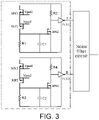
- a signal shaping circuit of the present disclosure includes a turn-on signal shaping module and a turn-off signal shaping module.
- the turn-on signal shaping module includes a first PMOS transistor MP1, a first NMOS transistor MN1, a second NMOS transistor MN2, a first resistor R1, a second resistor R2, a first capacitor C1, and a first inverter INV1.
- a gate of the first PMOS transistor MP1 is connected with a first input signal Vput1, a drain of the first PMOS transistor MP1 is respectively connected with a first end of the first resistor R1, a first end of the first capacitor C1, and a gate of the second NMOS transistor MN2, and a source of the first PMOS transistor MP1 is connected with a source of the first NMOS transistor MN1.
- a gate of the first NMOS transistor MN1 is connected with a second input signal Vput2, and a drain of the first NMOS transistor MN1 and a first end of the second resistor R2 are both connected with a reference voltage VB.
- a drain of the second NMOS transistor MN2 is connected with a second end of the second resistor R2, and a source of the second NMOS transistor MN2, a second end of the first resistor R1, and a second end of the first capacitor C1 are all grounded.
- An input end of the first inverter INV1 is connected with a second end of the second resistor R2, a voltage end of the first inverter INV1 is connected with the reference voltage VB, a ground end of the first inverter INV1 is grounded, and an output end of the first inverter INV1 constitutes a first output end of the signal shaping circuit.
- the turn-off signal shaping module includes a second PMOS transistor MP2, a third NMOS transistor MN3, a fourth NMOS transistor MN4, a third resistor R3, a fourth resistor R4, a second capacitor C2, and a second inverter INV2.
- a gate of the second PMOS transistor MP2 is connected with the second input signal Vput2, a drain of the second PMOS transistor MP2 is respectively connected with a first end of the third resistor R3, a first end of the second capacitor C2, and a gate of the fourth NMOS transistor MN4, and a source of the second PMOS transistor MP2 is connected with a source of the third NMOS transistor MN3.
- a gate of the third NMOS transistor MN3 is connected with the first input signal Vput1, and a drain of the third NMOS transistor MN3 and a first end of the fourth resistor R4 are both connected with the reference voltage VB.
- a drain of the fourth NMOS transistor MN4 is connected with a second end of the fourth resistor R4, and a source of the fourth NMOS transistor MN4, a second end of the third resistor R3, and a second end of the second capacitor C2 are all grounded.
- An input end of the second inverter INV2 is connected with a second end of the fourth resistor R4, a voltage end of the second inverter INV2 is connected with the reference voltage VB, a ground end of the second inverter INV2 is grounded, and an output end of the second inverter INV2 constitutes a second output end of the signal shaping circuit.
- a signal shaping circuit of the present disclosure is further provided with a third PMOS transistor MP3, a fifth NMOS transistor MN5, a sixth NMOS transistor MN6, and a fifth resistor R5 in the turn-on signal shaping module.
- a gate of the third PMOS transistor MP3 is connected with the second input signal Vput2, and a drain of the third PMOS transistor MP3 is respectively connected with a drain and a gate of the fifth NMOS transistor MN5 and a gate of the sixth NMOS transistor MN6; a source of the third PMOS transistor MP3 is connected with the reference voltage VB through the fifth resistor R5.
- a source of the fifth NMOS transistor MN5 and a source of the sixth NMOS transistor MN6 are both grounded.
- a drain of the sixth NMOS transistor MN6 is connected with a drain of the first PMOS transistor MP1.
- the turn-off signal shaping module is further provided with a fourth PMOS transistor MP4, a seventh NMOS transistor MN7, an eighth NMOS transistor MN8, and a sixth resistor R6.
- a gate of the fourth PMOS transistor MP4 is connected with the first input signal Vput1, and a drain of the fourth PMOS transistor MP4 is respectively connected with a drain and a gate of the seventh NMOS transistor MN7 and a gate of the eighth NMOS transistor MN8; a source of the fourth PMOS transistor MP4 is connected with the reference voltage VB through the sixth resistor R6.
- a source of the seventh NMOS transistor MN7 and a source of the eighth NMOS transistor MN8 are both grounded.
- a drain of the eighth NMOS transistor MN8 is connected with a drain of the second PMOS transistor MP2.
- Performance of the signal shaping circuit in the embodiment of Fig. 4 is better than the signal shaping circuit in the embodiment of Fig. 3 .
- the circuit in Fig. 3 can also output corresponding signals according to the first input signal Vput1 and the second input signal Vput2 to achieve the effect of eliminating offset noise.
- the circuit in Fig. 3 can only provide a pull-down function through the first resistor R1 and the third resistor R3, the pull-down capability is weak, and anti-interference performance is not as good as the signal shaping circuit in the embodiment in Fig. 4 .
- the upper part of the circuit includes a first PMOS transistor MP1, a first NMOS transistor MN1, a second NMOS transistor MN2, a first resistor R1, a second resistor R2, a first capacitor C1, a first inverter INV1, a third PMOS transistor MP3, a fifth NMOS transistor MN5, a sixth NMOS transistor MN6, and a fifth resistor R5.
- the first PMOS transistor MP1, the first NMOS transistor MN1, the third PMOS transistor MP3, the fifth NMOS transistor MN5, and the sixth NMOS transistor MN6 form a signal input stage structure.
- the fifth NMOS transistor MN5 and the sixth NMOS transistor MN6 form a current mirror.
- the first PMOS transistor MP1 and the third PMOS transistor MP3 form a differential pair input structure. As shown in Fig. 4 , one first NMOS transistor MN1 is connected in series to the first PMOS transistor MP1, and the same input signal is connected with gates of the first NMOS transistor MN1 and the third PMOS transistor MP3.
- the first PMOS transistor MP1 and the first NMOS transistor MN1 are turned on at the same time only when a difference between the first input signal Vput1 and the second input signal Vput2 needs to at least exceed a sum of thresholds of the first PMOS transistor MP1 and the first NMOS transistor MN1 (assuming that the threshold of the first NMOS transistor MN1 is Vthn1, thresholds of the first PMOS transistor MP1 and the third PMOS transistor MP3 are both Vthp1, then a sum of the thresholds of the first PMOS transistor MP1 and the first NMOS transistor MN1 is Vthn1 + Vthp1).
- the circuit is further provided with a first resistor R1 and a first capacitor C1.
- an amplitude of a differential signal inputted to the circuit needs to be higher than the sum of the thresholds of the first PMOS transistor MP1 and the first NMOS transistor MN1 for a certain period of time to generate a second-stage input signal.
- some interference or offset noise caused by device mismatch can be effectively filtered out.
- a first output end and a second output end of the signal shaping circuit in Fig. 3 and Fig. 4 are both connected with a post-stage noise filter circuit.
- the above-mentioned signal shaping circuit can also be applied to other situations, and is connected with a corresponding circuit of a subsequent stage.
- a gate driving circuit including the above-mentioned signal shaping circuit further includes:
- the level shift circuit includes a ninth NMOS transistor MN9 and a tenth NMOS transistor MN10, and the ninth NMOS transistor MN9 and the tenth NMOS transistor MN10 are two high-voltage NMOS transistors.
- a gate of the ninth NMOS transistor MN9 is connected with the pulse-on signal Von, a source of the ninth NMOS transistor MN9 is grounded, and a drain of the ninth NMOS transistor MN9 is respectively connected with a first end of the seventh resistor R7 and an anode of the first Zener diode Z1.
- a second end of the seventh resistor R7 and a cathode of the first Zener diode Z1 are both connected with the reference voltage VB.
- a drain of the ninth NMOS transistor MN9 is further served as a first output end of the level shift circuit to output the first input signal Vput1.
- a gate of the tenth NMOS transistor MN10 is connected with the pulse-off signal Voff, a source of the tenth NMOS transistor MN10 is grounded, and a drain of the tenth NMOS transistor MN10 is respectively connected with a first end of the eighth resistor R8 and an anode of the second Zener diode Z2.
- a second end of the eighth resistor R8 and a cathode of the second Zener diode Z2 are both connected with the reference voltage VB.
- a drain of the tenth NMOS transistor MN10 is further served as a second output end of the level shift circuit to output the second input signal Vput2.
- a working principle of the level shift circuit is as follows:
- a pull-down current is generated to pass through the seventh resistor R7, and a voltage signal relative to the reference voltage VB, namely, the first input signal Vput1, is generated.
- a pull-down current is generated to pass through the eighth resistor R8, and a voltage signal relative to the reference voltage VB, namely, the second input signal Vput2, is generated.
- the first Zener diode Z1 and the second Zener diode Z2 are used for clamping to prevent the first input signal Vput1 and the second input signal Vput2 from falling too much relative to the reference voltage VB, thus avoiding damage to the circuit.
- a noise filter circuit is configured to further eliminate short-pulse noise in a signal outputted by the signal shaping circuit.
- the noise filter circuit includes a first inverter chain, a ninth resistor R9, a third capacitor C3, a first Schmitt trigger SIMT1, a second inverter chain, a tenth resistor R10, a fourth capacitor C4, and a second Schmitt trigger SIMT2.
- An input end of the first inverter chain is connected with a first output end of the signal shaping circuit.
- An output end of the first inverter chain is connected with a first end of the ninth resistor R9.
- a second end of the ninth resistor R9 is respectively connected with a first end of the third capacitor C3 and an input end of the first Schmitt trigger SIMT1.
- a second end of the third capacitor C3 is grounded.
- An output end of the first Schmitt trigger SIMT1 constitutes a first output end of the noise filter circuit, and is connected with a first input end of the output stage driving circuit.
- An input end of the second inverter chain is connected with a second output end of the signal shaping circuit.
- An output end of the second inverter chain is connected with a first end of the tenth resistor R10.
- a second end of the tenth resistor R10 is respectively connected with a first end of the fourth capacitor C4 and an input end of the second Schmitt trigger SIMT2.
- a second end of the fourth capacitor C4 is grounded.
- An output end of the second Schmitt trigger SIMT2 constitutes a second output end of the noise filter circuit, and is connected with a second input end of the output stage driving circuit.
- the ninth resistor R9 and the third capacitor C3 form a filter circuit to further filter a signal outputted by a previous-stage signal shaping circuit to eliminate a short-pulse noise signal.
- the output stage driving circuit is connected with the noise filter circuit and outputs a gate driving signal OUT.
- the output stage driving circuit includes a first NAND gate NAND1, a third inverter chain, a fifth PMOS transistor MP5, an eleventh resistor R11, a second NAND gate NAND2, a fourth inverter chain, an eleventh NMOS transistor MN11, and a twelfth resistor R12.
- a first end of the first NAND gate NAND1 constitutes a first input end of the output stage driving circuit.
- An output end of the first NAND gate NAND1 is respectively connected with an input end of the third inverter chain and a second end of the second NAND gate NAND2.
- An output end of the third inverter chain is connected with a gate of the fifth PMOS transistor MP5.
- a source of the fifth PMOS transistor MP5 is connected with the reference voltage VB, and a drain of the fifth PMOS transistor MP5 is connected with a first end of the eleventh resistor R11.
- a first end of the second NAND gate NAND2 constitutes a second input end of the output stage driving circuit.
- An output end of the second NAND gate NAND2 is respectively connected with an input end of the fourth inverter chain and a second end of the first NAND gate NAND1.
- An output end of the fourth inverter chain is connected with a gate of the eleventh NMOS transistor MN11.
- a source of the eleventh NMOS transistor MN11 is grounded, and a drain of the eleventh NMOS transistor MN11 is connected with a first end of the twelfth resistor R12.
- an RS flip-flop formed by the first NAND gate NAND1 and the second NAND gate NAND2 can effectively lock and save an effective pulse input signal.
- a final gate driving signal OUT is generated after the pulse input signal passes through the fifth PMOS transistor, the eleventh NMOS transistor, the eleventh resistor R11, and the twelfth resistor R12 in the subsequent stage.
- FIG. 6 for structures of the noise filter circuit and the output stage driving circuit in this embodiment, where the first inverter chain, the second inverter chain, the third inverter chain, and the fourth inverter chain can all include cascaded inverters.
- End A and end B in the noise filter circuit in FIG. 6 are respectively connected with end A and end B in Fig. 3 or Fig. 4 .
- the output stage driving circuit can also be implemented by a circuit groove shown in FIG. 7 , which includes a third NAND gate NAND3, a fourth NAND gate NAND4, a fifth inverter chain, a sixth inverter chain, a twelfth NMOS transistor MN12, a thirteenth NMOS transistor MN13, and a fourteenth NMOS transistor MN14, a fifteenth NMOS transistor MN15, a sixth PMOS transistor MP6, a seventh PMOS transistor MP7, an eighth PMOS transistor MP8, and a ninth PMOS transistor MP9.
- a first end of the third NAND gate NAND3 constitutes a first input end of the output stage driving circuit.
- An output end of the third NAND gate NAND3 is respectively connected with an input end of the fifth inverter chain and a second end of the fourth NAND gate NAND4.
- a first end of the fourth NAND gate NAND4 constitutes a second input end of the output stage driving circuit, and an output end of the fourth NAND gate NAND4 is connected with a second end of the third NAND gate NAND3.
- An output end of the fifth inverter chain is respectively connected with an input end of the sixth inverter chain, a gate of the seventh PMOS transistor MP7, and a gate of the fourteenth NMOS transistor MN14.
- An output end of the sixth inverter chain is respectively connected with a drain of the twelfth NMOS transistor MN12, a gate of the thirteenth NMOS transistor MN13, a drain of the sixth PMOS transistor MP6, and a gate of the eighth PMOS transistor MP8.
- a drain of the seventh PMOS transistor MP7 is respectively connected with a drain of the thirteenth NMOS transistor MN13, a gate of the ninth PMOS transistor MP9, and a gate of the sixth PMOS transistor MP6.
- a drain of the fourteenth NMOS transistor MN14 is respectively connected with a drain of the eighth PMOS transistor MP8, a gate of the fifteenth NMOS transistor MN15, and a gate of the twelfth NMOS transistor MN12.
- a source of the seventh PMOS transistor MP7, a source of the eighth PMOS transistor MP8, and a source of the ninth PMOS transistor MP9 are all connected with the reference voltage VB.
- a source of the twelfth NMOS transistor MN12, a source of the thirteenth NMOS transistor MN13, a source of the fourteenth NMOS transistor MN14, and a source of the fifteenth NMOS transistor MN15 are all grounded.
- the fifth inverter chain and the sixth inverter chain may include cascaded inverters.
- the output stage driving circuit in this embodiment respectively controls the ninth PMOS transistor MP9 and the fifteenth NMOS transistor MN15, which can prevent a passing-through current from damaging an output stage circuit, uses a two-stage inverter chain (the fifth inverter chain and the sixth inverter chain) to produce an extremely short dead time, and achieves a clamping effect through the sixth PMOS transistor MP6 and the twelfth NMOS transistor MN12 to avoid device damage caused by passing-through current resulted from the crossover of gate driving signals of devices in the output stage circuit, thereby achieving a minimal transmission delay and low circuit noise while ensuring the reliability.
- the control circuit can adapt to different application environments and has high reliability.
- the gate driving circuit in this embodiment can resist noise interference, and reduce the impact of offset noise, so that the circuit works more reliably.
- the circuit has a simple structure, stable performance and strong adaptability.
- An additional NMOS transistor is added to the signal shaping circuit, which improves requirements for the amplitude of an input differential signal.
- the amplitude of the input differential signal needs to be higher than a certain value for a certain period of time before being recognized as a trigger signal, and some interference or offset noise caused by device mismatch is effectively filtered out.
- a gate driving circuit using the signal shaping circuit further includes a pulse generating circuit, a level shift circuit, a noise filter circuit and an output stage driving circuit. The offset noise and common mode noise can be effectively filtered out through the cooperation of the circuits.
Landscapes
- Physics & Mathematics (AREA)
- Nonlinear Science (AREA)
- Logic Circuits (AREA)
- Electronic Switches (AREA)
- Amplifiers (AREA)
Applications Claiming Priority (2)
| Application Number | Priority Date | Filing Date | Title |
|---|---|---|---|
| CN201911212023.8A CN112994662B (zh) | 2019-12-02 | 2019-12-02 | 信号整形电路及相应的栅极驱动电路 |
| PCT/CN2020/133350 WO2021110043A1 (fr) | 2019-12-02 | 2020-12-02 | Circuit de mise en forme de signal et circuit d'attaque de grille correspondant |
Publications (4)
| Publication Number | Publication Date |
|---|---|
| EP4016843A1 true EP4016843A1 (fr) | 2022-06-22 |
| EP4016843A4 EP4016843A4 (fr) | 2022-10-12 |
| EP4016843B1 EP4016843B1 (fr) | 2023-11-08 |
| EP4016843C0 EP4016843C0 (fr) | 2023-11-08 |
Family
ID=76221430
Family Applications (1)
| Application Number | Title | Priority Date | Filing Date |
|---|---|---|---|
| EP20896816.4A Active EP4016843B1 (fr) | 2019-12-02 | 2020-12-02 | Circuit de mise en forme de signal et circuit d'attaque de grille correspondant |
Country Status (3)
| Country | Link |
|---|---|
| EP (1) | EP4016843B1 (fr) |
| CN (1) | CN112994662B (fr) |
| WO (1) | WO2021110043A1 (fr) |
Families Citing this family (13)
| Publication number | Priority date | Publication date | Assignee | Title |
|---|---|---|---|---|
| CN116047938B (zh) * | 2021-10-28 | 2025-11-11 | 华润微集成电路(无锡)有限公司 | 检测芯片、温度检测系统及湿度检测系统 |
| CN114583939B (zh) * | 2022-04-21 | 2025-12-05 | 西安航天民芯科技有限公司 | 一种用于高性能电源管理的超低压启动辅助电路 |
| CN114744997B (zh) * | 2022-06-08 | 2022-09-09 | 深圳芯能半导体技术有限公司 | 一种电平位移电路及集成电路 |
| CN115328246B (zh) * | 2022-08-12 | 2023-09-29 | 苏州大学 | 一种快速建立的低噪声基准电压源电路 |
| CN116827330B (zh) * | 2022-12-12 | 2024-03-12 | 南京微盟电子有限公司 | 强抗干扰通讯端口电路 |
| CN116169985B (zh) * | 2023-01-03 | 2025-07-25 | 深圳市美矽微半导体股份有限公司 | 一种具有电压与温度补偿的振荡电路 |
| CN116346120B (zh) * | 2023-05-29 | 2023-10-13 | 无锡市晶源微电子股份有限公司 | 电平转换电路 |
| CN117498854B (zh) * | 2023-09-20 | 2024-06-21 | 北京芯可鉴科技有限公司 | Igbt驱动电路及芯片 |
| CN117254682B (zh) * | 2023-11-20 | 2024-03-12 | 成都芯翼科技有限公司 | 一种抗干扰电压转换电路 |
| CN117477918B (zh) * | 2023-12-27 | 2024-03-29 | 成都氮矽科技有限公司 | 驱动信号输入检测电路、GaN栅驱动器和MOSFET栅驱动器 |
| CN119519687B (zh) * | 2024-11-07 | 2025-10-24 | 西安电子科技大学 | 一种具有对称式脉冲电流辅助结构的高压电平转换电路 |
| CN119134977B (zh) * | 2024-11-15 | 2025-05-27 | 上海紫鹰微电子有限公司 | 一种半桥驱动控制电路 |
| CN119543913B (zh) * | 2025-01-20 | 2025-04-04 | 苏州锴威特半导体股份有限公司 | 共模降噪电平位移电路 |
Family Cites Families (13)
| Publication number | Priority date | Publication date | Assignee | Title |
|---|---|---|---|---|
| TW293108B (fr) * | 1994-11-25 | 1996-12-11 | Hitachi Ltd | |
| KR101083093B1 (ko) * | 2004-09-03 | 2011-11-16 | 페어차일드코리아반도체 주식회사 | 게이트 드라이버 회로 |
| KR101573460B1 (ko) * | 2009-04-30 | 2015-12-02 | 삼성디스플레이 주식회사 | 게이트 구동회로 |
| CN101917811B (zh) * | 2010-08-02 | 2013-04-17 | 西安文理学院 | 一种抗噪声干扰的高端驱动电路 |
| EP2592381A1 (fr) * | 2011-11-08 | 2013-05-15 | EADS Construcciones Aeronauticas, S.A. | Dispositif de consolidation de signaux discrets et procédé et aéronef équipé de ce dispositif |
| CN102611425B (zh) * | 2012-03-08 | 2014-05-14 | 东南大学 | 一种抗电源噪声干扰的高压侧栅极驱动电路 |
| CN102647177B (zh) * | 2012-04-06 | 2014-05-14 | 东南大学 | 一种可抗共模噪声干扰的高压侧栅驱动电路 |
| CN105139816B (zh) * | 2015-09-24 | 2017-12-19 | 深圳市华星光电技术有限公司 | 栅极驱动电路 |
| CN106230416B (zh) * | 2016-07-14 | 2018-08-31 | 电子科技大学 | 一种带有源钳位的无自举栅极驱动电路 |
| KR20180106493A (ko) * | 2017-03-20 | 2018-10-01 | 에스케이하이닉스 주식회사 | 반도체장치 |
| CN107612528A (zh) * | 2017-09-29 | 2018-01-19 | 科域科技有限公司 | 一种脉冲滤波电路装置 |
| CN208079042U (zh) * | 2018-04-26 | 2018-11-09 | 无锡安趋电子有限公司 | 噪声消除电路及低延时高压侧驱动电路 |
| CN108288963B (zh) * | 2018-04-26 | 2023-09-05 | 无锡安趋电子有限公司 | 噪声消除电路及低延时高压侧驱动电路 |
-
2019
- 2019-12-02 CN CN201911212023.8A patent/CN112994662B/zh active Active
-
2020
- 2020-12-02 WO PCT/CN2020/133350 patent/WO2021110043A1/fr not_active Ceased
- 2020-12-02 EP EP20896816.4A patent/EP4016843B1/fr active Active
Also Published As
| Publication number | Publication date |
|---|---|
| EP4016843B1 (fr) | 2023-11-08 |
| WO2021110043A1 (fr) | 2021-06-10 |
| CN112994662A (zh) | 2021-06-18 |
| EP4016843C0 (fr) | 2023-11-08 |
| EP4016843A4 (fr) | 2022-10-12 |
| CN112994662B (zh) | 2023-03-14 |
Similar Documents
| Publication | Publication Date | Title |
|---|---|---|
| EP4016843B1 (fr) | Circuit de mise en forme de signal et circuit d'attaque de grille correspondant | |
| CN108288963B (zh) | 噪声消除电路及低延时高压侧驱动电路 | |
| CN102769453B (zh) | 一种可抗噪声干扰的高压侧栅驱动电路 | |
| CN109039029B (zh) | 一种适用于GaN功率器件栅驱动电路的自举充电电路 | |
| CN103762969B (zh) | 一种抗噪声干扰的高压侧栅驱动电路 | |
| KR100933651B1 (ko) | 하프-브릿지 드라이버 및 그러한 드라이버를 갖는 파워 변환 시스템 | |
| JP4327411B2 (ja) | 半導体装置 | |
| EP2873154B1 (fr) | Circuits et techniques connexes permettant de piloter le côté haut d'un circuit en demi-pont | |
| CN113965194B (zh) | 一种具有噪声检测的低延时高压侧驱动电路 | |
| US6130556A (en) | Integrated circuit I/O buffer with 5V well and passive gate voltage | |
| CN102647177B (zh) | 一种可抗共模噪声干扰的高压侧栅驱动电路 | |
| CN101083430A (zh) | 浮动驱动电路 | |
| WO2014171190A1 (fr) | Circuit de décalage de niveau | |
| CN118054782A (zh) | 提升高压栅驱动芯片抗噪能力的电平移位电路 | |
| CN117394844A (zh) | 电平移位电路、驱动电路和半桥电路 | |
| CN114640331B (zh) | 一种抗噪声干扰的高压侧栅驱动电路 | |
| Zhang et al. | A capacitive-loaded level shift circuit for improving the noise immunity of high voltage gate drive IC | |
| US7626441B2 (en) | Drive circuit with BOT level shifter for transmitting an input signal and assigned method | |
| CN116865208A (zh) | 欠压保护电路 | |
| CN113472185B (zh) | 一种适用于高压GaN半桥栅驱动系统的电平移位电路 | |
| CN109687861B (zh) | 一种抗噪声的高压栅驱动电路 | |
| CN116885923A (zh) | 一种高dv/dt噪声抑制的高压侧驱动电路 | |
| WO2025251646A1 (fr) | Circuit de décalage de niveau à forte immunité au bruit et à faible retard pour puce d'attaque en demi-pont en gan | |
| US10797704B2 (en) | Differential signal transfer systems and associated methods | |
| CN114640339A (zh) | 一种无上电不定态的电平转换电路 |
Legal Events
| Date | Code | Title | Description |
|---|---|---|---|
| STAA | Information on the status of an ep patent application or granted ep patent |
Free format text: STATUS: THE INTERNATIONAL PUBLICATION HAS BEEN MADE |
|
| PUAI | Public reference made under article 153(3) epc to a published international application that has entered the european phase |
Free format text: ORIGINAL CODE: 0009012 |
|
| STAA | Information on the status of an ep patent application or granted ep patent |
Free format text: STATUS: REQUEST FOR EXAMINATION WAS MADE |
|
| 17P | Request for examination filed |
Effective date: 20220316 |
|
| AK | Designated contracting states |
Kind code of ref document: A1 Designated state(s): AL AT BE BG CH CY CZ DE DK EE ES FI FR GB GR HR HU IE IS IT LI LT LU LV MC MK MT NL NO PL PT RO RS SE SI SK SM TR |
|
| REG | Reference to a national code |
Ref country code: DE Ref legal event code: R079 Free format text: PREVIOUS MAIN CLASS: H03K0005010000 Ipc: H03K0005125200 Ref document number: 602020020887 Country of ref document: DE |
|
| A4 | Supplementary search report drawn up and despatched |
Effective date: 20220913 |
|
| RIC1 | Information provided on ipc code assigned before grant |
Ipc: H03K 19/0185 20060101ALN20220907BHEP Ipc: H03K 5/151 20060101ALI20220907BHEP Ipc: H03K 5/1252 20060101AFI20220907BHEP |
|
| DAV | Request for validation of the european patent (deleted) | ||
| DAX | Request for extension of the european patent (deleted) | ||
| RIC1 | Information provided on ipc code assigned before grant |
Ipc: H03K 19/0185 20060101ALN20230406BHEP Ipc: H03K 5/151 20060101ALI20230406BHEP Ipc: H03K 5/1252 20060101AFI20230406BHEP |
|
| GRAP | Despatch of communication of intention to grant a patent |
Free format text: ORIGINAL CODE: EPIDOSNIGR1 |
|
| STAA | Information on the status of an ep patent application or granted ep patent |
Free format text: STATUS: GRANT OF PATENT IS INTENDED |
|
| INTG | Intention to grant announced |
Effective date: 20230524 |
|
| GRAS | Grant fee paid |
Free format text: ORIGINAL CODE: EPIDOSNIGR3 |
|
| GRAA | (expected) grant |
Free format text: ORIGINAL CODE: 0009210 |
|
| STAA | Information on the status of an ep patent application or granted ep patent |
Free format text: STATUS: THE PATENT HAS BEEN GRANTED |
|
| AK | Designated contracting states |
Kind code of ref document: B1 Designated state(s): AL AT BE BG CH CY CZ DE DK EE ES FI FR GB GR HR HU IE IS IT LI LT LU LV MC MK MT NL NO PL PT RO RS SE SI SK SM TR |
|
| REG | Reference to a national code |
Ref country code: GB Ref legal event code: FG4D |
|
| REG | Reference to a national code |
Ref country code: CH Ref legal event code: EP |
|
| REG | Reference to a national code |
Ref country code: DE Ref legal event code: R096 Ref document number: 602020020887 Country of ref document: DE |
|
| REG | Reference to a national code |
Ref country code: IE Ref legal event code: FG4D |
|
| U01 | Request for unitary effect filed |
Effective date: 20231130 |
|
| U07 | Unitary effect registered |
Designated state(s): AT BE BG DE DK EE FI FR IT LT LU LV MT NL PT SE SI Effective date: 20231218 |
|
| U20 | Renewal fee for the european patent with unitary effect paid |
Year of fee payment: 4 Effective date: 20231219 |
|
| PG25 | Lapsed in a contracting state [announced via postgrant information from national office to epo] |
Ref country code: GR Free format text: LAPSE BECAUSE OF FAILURE TO SUBMIT A TRANSLATION OF THE DESCRIPTION OR TO PAY THE FEE WITHIN THE PRESCRIBED TIME-LIMIT Effective date: 20240209 |
|
| PG25 | Lapsed in a contracting state [announced via postgrant information from national office to epo] |
Ref country code: IS Free format text: LAPSE BECAUSE OF FAILURE TO SUBMIT A TRANSLATION OF THE DESCRIPTION OR TO PAY THE FEE WITHIN THE PRESCRIBED TIME-LIMIT Effective date: 20240308 |
|
| PG25 | Lapsed in a contracting state [announced via postgrant information from national office to epo] |
Ref country code: ES Free format text: LAPSE BECAUSE OF FAILURE TO SUBMIT A TRANSLATION OF THE DESCRIPTION OR TO PAY THE FEE WITHIN THE PRESCRIBED TIME-LIMIT Effective date: 20231108 |
|
| PG25 | Lapsed in a contracting state [announced via postgrant information from national office to epo] |
Ref country code: IS Free format text: LAPSE BECAUSE OF FAILURE TO SUBMIT A TRANSLATION OF THE DESCRIPTION OR TO PAY THE FEE WITHIN THE PRESCRIBED TIME-LIMIT Effective date: 20240308 Ref country code: GR Free format text: LAPSE BECAUSE OF FAILURE TO SUBMIT A TRANSLATION OF THE DESCRIPTION OR TO PAY THE FEE WITHIN THE PRESCRIBED TIME-LIMIT Effective date: 20240209 Ref country code: ES Free format text: LAPSE BECAUSE OF FAILURE TO SUBMIT A TRANSLATION OF THE DESCRIPTION OR TO PAY THE FEE WITHIN THE PRESCRIBED TIME-LIMIT Effective date: 20231108 |
|
| PG25 | Lapsed in a contracting state [announced via postgrant information from national office to epo] |
Ref country code: RS Free format text: LAPSE BECAUSE OF FAILURE TO SUBMIT A TRANSLATION OF THE DESCRIPTION OR TO PAY THE FEE WITHIN THE PRESCRIBED TIME-LIMIT Effective date: 20231108 Ref country code: PL Free format text: LAPSE BECAUSE OF FAILURE TO SUBMIT A TRANSLATION OF THE DESCRIPTION OR TO PAY THE FEE WITHIN THE PRESCRIBED TIME-LIMIT Effective date: 20231108 Ref country code: NO Free format text: LAPSE BECAUSE OF FAILURE TO SUBMIT A TRANSLATION OF THE DESCRIPTION OR TO PAY THE FEE WITHIN THE PRESCRIBED TIME-LIMIT Effective date: 20240208 Ref country code: HR Free format text: LAPSE BECAUSE OF FAILURE TO SUBMIT A TRANSLATION OF THE DESCRIPTION OR TO PAY THE FEE WITHIN THE PRESCRIBED TIME-LIMIT Effective date: 20231108 |
|
| PG25 | Lapsed in a contracting state [announced via postgrant information from national office to epo] |
Ref country code: CZ Free format text: LAPSE BECAUSE OF FAILURE TO SUBMIT A TRANSLATION OF THE DESCRIPTION OR TO PAY THE FEE WITHIN THE PRESCRIBED TIME-LIMIT Effective date: 20231108 |
|
| PG25 | Lapsed in a contracting state [announced via postgrant information from national office to epo] |
Ref country code: SK Free format text: LAPSE BECAUSE OF FAILURE TO SUBMIT A TRANSLATION OF THE DESCRIPTION OR TO PAY THE FEE WITHIN THE PRESCRIBED TIME-LIMIT Effective date: 20231108 |
|
| PG25 | Lapsed in a contracting state [announced via postgrant information from national office to epo] |
Ref country code: SM Free format text: LAPSE BECAUSE OF FAILURE TO SUBMIT A TRANSLATION OF THE DESCRIPTION OR TO PAY THE FEE WITHIN THE PRESCRIBED TIME-LIMIT Effective date: 20231108 Ref country code: SK Free format text: LAPSE BECAUSE OF FAILURE TO SUBMIT A TRANSLATION OF THE DESCRIPTION OR TO PAY THE FEE WITHIN THE PRESCRIBED TIME-LIMIT Effective date: 20231108 Ref country code: RO Free format text: LAPSE BECAUSE OF FAILURE TO SUBMIT A TRANSLATION OF THE DESCRIPTION OR TO PAY THE FEE WITHIN THE PRESCRIBED TIME-LIMIT Effective date: 20231108 Ref country code: CZ Free format text: LAPSE BECAUSE OF FAILURE TO SUBMIT A TRANSLATION OF THE DESCRIPTION OR TO PAY THE FEE WITHIN THE PRESCRIBED TIME-LIMIT Effective date: 20231108 |
|
| REG | Reference to a national code |
Ref country code: CH Ref legal event code: PL |
|
| REG | Reference to a national code |
Ref country code: DE Ref legal event code: R097 Ref document number: 602020020887 Country of ref document: DE |
|
| PG25 | Lapsed in a contracting state [announced via postgrant information from national office to epo] |
Ref country code: MC Free format text: LAPSE BECAUSE OF FAILURE TO SUBMIT A TRANSLATION OF THE DESCRIPTION OR TO PAY THE FEE WITHIN THE PRESCRIBED TIME-LIMIT Effective date: 20231108 |
|
| PG25 | Lapsed in a contracting state [announced via postgrant information from national office to epo] |
Ref country code: MC Free format text: LAPSE BECAUSE OF FAILURE TO SUBMIT A TRANSLATION OF THE DESCRIPTION OR TO PAY THE FEE WITHIN THE PRESCRIBED TIME-LIMIT Effective date: 20231108 |
|
| PLBE | No opposition filed within time limit |
Free format text: ORIGINAL CODE: 0009261 |
|
| STAA | Information on the status of an ep patent application or granted ep patent |
Free format text: STATUS: NO OPPOSITION FILED WITHIN TIME LIMIT |
|
| REG | Reference to a national code |
Ref country code: IE Ref legal event code: MM4A |
|
| PG25 | Lapsed in a contracting state [announced via postgrant information from national office to epo] |
Ref country code: IE Free format text: LAPSE BECAUSE OF NON-PAYMENT OF DUE FEES Effective date: 20231202 |
|
| 26N | No opposition filed |
Effective date: 20240809 |
|
| PG25 | Lapsed in a contracting state [announced via postgrant information from national office to epo] |
Ref country code: CH Free format text: LAPSE BECAUSE OF NON-PAYMENT OF DUE FEES Effective date: 20231231 |
|
| PG25 | Lapsed in a contracting state [announced via postgrant information from national office to epo] |
Ref country code: IE Free format text: LAPSE BECAUSE OF NON-PAYMENT OF DUE FEES Effective date: 20231202 Ref country code: CH Free format text: LAPSE BECAUSE OF NON-PAYMENT OF DUE FEES Effective date: 20231231 |
|
| U20 | Renewal fee for the european patent with unitary effect paid |
Year of fee payment: 5 Effective date: 20241009 |
|
| PG25 | Lapsed in a contracting state [announced via postgrant information from national office to epo] |
Ref country code: CY Free format text: LAPSE BECAUSE OF FAILURE TO SUBMIT A TRANSLATION OF THE DESCRIPTION OR TO PAY THE FEE WITHIN THE PRESCRIBED TIME-LIMIT; INVALID AB INITIO Effective date: 20201202 |
|
| PG25 | Lapsed in a contracting state [announced via postgrant information from national office to epo] |
Ref country code: HU Free format text: LAPSE BECAUSE OF FAILURE TO SUBMIT A TRANSLATION OF THE DESCRIPTION OR TO PAY THE FEE WITHIN THE PRESCRIBED TIME-LIMIT; INVALID AB INITIO Effective date: 20201202 |
|
| GBPC | Gb: european patent ceased through non-payment of renewal fee |
Effective date: 20241202 |
|
| PG25 | Lapsed in a contracting state [announced via postgrant information from national office to epo] |
Ref country code: GB Free format text: LAPSE BECAUSE OF NON-PAYMENT OF DUE FEES Effective date: 20241202 |
|
| PG25 | Lapsed in a contracting state [announced via postgrant information from national office to epo] |
Ref country code: TR Free format text: LAPSE BECAUSE OF FAILURE TO SUBMIT A TRANSLATION OF THE DESCRIPTION OR TO PAY THE FEE WITHIN THE PRESCRIBED TIME-LIMIT Effective date: 20231108 |
|
| U20 | Renewal fee for the european patent with unitary effect paid |
Year of fee payment: 6 Effective date: 20251230 |