EP4020146A1 - Procédé d'analyse de fréquence de détection tactile pour écrans tactiles capacitifs projetés - Google Patents
Procédé d'analyse de fréquence de détection tactile pour écrans tactiles capacitifs projetés Download PDFInfo
- Publication number
- EP4020146A1 EP4020146A1 EP21211887.1A EP21211887A EP4020146A1 EP 4020146 A1 EP4020146 A1 EP 4020146A1 EP 21211887 A EP21211887 A EP 21211887A EP 4020146 A1 EP4020146 A1 EP 4020146A1
- Authority
- EP
- European Patent Office
- Prior art keywords
- row
- touch
- column
- conductors
- signals
- Prior art date
- Legal status (The legal status is an assumption and is not a legal conclusion. Google has not performed a legal analysis and makes no representation as to the accuracy of the status listed.)
- Withdrawn
Links
Images



Classifications
-
- G—PHYSICS
- G06—COMPUTING OR CALCULATING; COUNTING
- G06F—ELECTRIC DIGITAL DATA PROCESSING
- G06F3/00—Input arrangements for transferring data to be processed into a form capable of being handled by the computer; Output arrangements for transferring data from processing unit to output unit, e.g. interface arrangements
- G06F3/01—Input arrangements or combined input and output arrangements for interaction between user and computer
- G06F3/03—Arrangements for converting the position or the displacement of a member into a coded form
- G06F3/041—Digitisers, e.g. for touch screens or touch pads, characterised by the transducing means
- G06F3/044—Digitisers, e.g. for touch screens or touch pads, characterised by the transducing means by capacitive means
-
- G—PHYSICS
- G06—COMPUTING OR CALCULATING; COUNTING
- G06F—ELECTRIC DIGITAL DATA PROCESSING
- G06F3/00—Input arrangements for transferring data to be processed into a form capable of being handled by the computer; Output arrangements for transferring data from processing unit to output unit, e.g. interface arrangements
- G06F3/01—Input arrangements or combined input and output arrangements for interaction between user and computer
- G06F3/03—Arrangements for converting the position or the displacement of a member into a coded form
- G06F3/041—Digitisers, e.g. for touch screens or touch pads, characterised by the transducing means
- G06F3/0416—Control or interface arrangements specially adapted for digitisers
- G06F3/04164—Connections between sensors and controllers, e.g. routing lines between electrodes and connection pads
-
- G—PHYSICS
- G06—COMPUTING OR CALCULATING; COUNTING
- G06F—ELECTRIC DIGITAL DATA PROCESSING
- G06F3/00—Input arrangements for transferring data to be processed into a form capable of being handled by the computer; Output arrangements for transferring data from processing unit to output unit, e.g. interface arrangements
- G06F3/01—Input arrangements or combined input and output arrangements for interaction between user and computer
- G06F3/03—Arrangements for converting the position or the displacement of a member into a coded form
- G06F3/041—Digitisers, e.g. for touch screens or touch pads, characterised by the transducing means
- G06F3/0416—Control or interface arrangements specially adapted for digitisers
- G06F3/04166—Details of scanning methods, e.g. sampling time, grouping of sub areas or time sharing with display driving
-
- G—PHYSICS
- G06—COMPUTING OR CALCULATING; COUNTING
- G06F—ELECTRIC DIGITAL DATA PROCESSING
- G06F3/00—Input arrangements for transferring data to be processed into a form capable of being handled by the computer; Output arrangements for transferring data from processing unit to output unit, e.g. interface arrangements
- G06F3/01—Input arrangements or combined input and output arrangements for interaction between user and computer
- G06F3/03—Arrangements for converting the position or the displacement of a member into a coded form
- G06F3/041—Digitisers, e.g. for touch screens or touch pads, characterised by the transducing means
- G06F3/044—Digitisers, e.g. for touch screens or touch pads, characterised by the transducing means by capacitive means
- G06F3/0446—Digitisers, e.g. for touch screens or touch pads, characterised by the transducing means by capacitive means using a grid-like structure of electrodes in at least two directions, e.g. using row and column electrodes
Definitions
- the subject matter disclosed herein relates generally to touchscreen technology, and more particularly to frequency analysis methods of touch detection for projected capacitive (PCAP) touch sensors to enable their use in avionics environments, both in civil certified and other high-criticality installations.
- PCAP projected capacitive
- Multi-touch input is an expected and requested feature for new display products across military and commercial avionics market segments.
- Touch technology enables improved cockpit usability and crew efficiency, with consumer electronic experiences forming expectations for the user interface.
- PCAP touch sensors provide a user-friendly experience with gesturing, light touch, and multi-touch capabilities.
- susceptibility to electromagnetic interference (EMI) causing false touch event detection has prevented their adoption in avionics displays.
- PCAP touch sensors offer additional advantages in terms of reliability due to solid state construction and optical improvements including reduced reflection and improved contrast as compared to resistive touch sensors.
- a touch sensor For PCAP devices, a common touch sensor configuration includes a set of conductors arranged and connected to form rows and columns, wherein the rows and columns are electrically isolated. The points at which the row signals cross over the column signals form nodes. To detect touch events, the controller interacts with the touch sensor to measure the capacitance of each node. When the controller encounters a significant change in the measured capacitance of a node, the change is analyzed to determine if a touch event is occurring. The change in capacitance due to a touch is much lower than the overall capacitance of the touch system, which makes the measurement difficult.
- Methods for measuring capacitance in touch sensors include relaxation oscillators, charge time, charge transfer, sigma-delta modulation, successive approximation, and resonance change. Each of these methods employs a different method of measuring capacitance to determine the small change induced by a touch.
- the present disclosure provides a method of touch detection for a projected capacitive (PCAP) touch sensor comprising a network of row conductors and column conductors capacitively coupled at a plurality of nodes.
- PCAP projected capacitive
- the method includes generating a frequency set including a plurality of sine wave signals each characterized by a unique row frequency, transmitting the plurality of sine wave signals to the row conductors according to a predetermined rolling frequency scheme, receiving column signals from the column conductors each a summation of the unique row frequencies transmitted on the row conductors, processing the column signals using an algorithm (e.g., fast Fourier transform (FFT) algorithm) to deconstruct each column signal into the unique row frequencies transmitted on the row conductors and the magnitude of each frequency, analyzing the relative magnitudes of the unique row frequencies of the deconstructed column signals, and determining the presence of a touch at one of the plurality of nodes based on a change in the relative magnitude of one of the unique row frequencies.
- FFT fast Fourier transform
- the method may further include mapping a status of each of the plurality of nodes including recording the magnitude of the unique row frequency at each respective node and/or reporting a touch event to a coupled processor.
- the rotating frequency scheme for the row conductors requires that each transmitted sine wave signal for each row conductor be different from the most recently transmitted sine wave signal for that same row conductor.
- the frequency spacing between each of the plurality of sine wave signals is equal.
- each of the generating, transmitting, receiving and processing steps may be implemented on a touch controller comprising a plurality of electronic components, and the touch controller may be implemented as one of a microcontroller, a field programmable gate array (FPGA), and an application specific integrated circuit (ASIC).
- a touch controller comprising a plurality of electronic components
- the touch controller may be implemented as one of a microcontroller, a field programmable gate array (FPGA), and an application specific integrated circuit (ASIC).
- FPGA field programmable gate array
- ASIC application specific integrated circuit
- the present disclosure provides a PCAP touch system including first and second touch sensors each comprising row conductors and column conductors capacitively coupled at nodes formed at row-column conductor intersections such that signals transmitted on the row conductors propagate to the column conductors at capacitive connections of the nodes, and first and second touch controllers, wherein the first touch controller is coupled to the first touch sensor and the second touch controller is coupled to the second touch sensor, and wherein the first touch sensor and the first controller function independently of the second touch sensor and the second controller.
- the frequency set generated by the first controller may be different from the frequency set of the second controller such that the first and second touch controllers can operate on the respective first and second touch sensors in close proximity without interference.
- the first and second touch sensors may be implemented in a display wherein the first and second touch sensors are separate and positioned side-by-side.
- the first and second touch sensors may be implemented in a display wherein their row conductors and their column conductors are interleaved such that a first set of every other row conductor and every other column conductor is coupled to the first controller, and a second set of every other row conductor and every other column conductor is coupled to the second controller.
- any reference to “one embodiment” or “some embodiments” means that a particular element, feature, structure, or characteristic described in connection with the embodiment is included in at least one embodiment disclosed herein.
- the appearances of the phrase “in some embodiments” in various places in the specification are not necessarily all referring to the same embodiment, and embodiments may include one or more of the features expressly described or inherently present herein, or any combination or sub-combination of two or more such features, along with any other features which may not necessarily be expressly described or inherently present in the instant disclosure.
- the present disclosure describes a frequency analysis method for touch detection in PCAP touch sensors, a touch controller for implementing the touch detection method, and touchscreen devices including dual touch sensors and controllers for redundancy.
- a touch sensing system 100 generally includes a touch sensor 102 and a touch controller 104 coupled to the touch sensor 102.
- the touch sensor 102 generally includes a predetermined number of row conductors 106, illustrated as row conductors F0, F1, F2... Fn, and a predetermined number of column conductors 108, wherein the number of row conductors and the number of column conductors may or may not correspond.
- the row conductors 106 and the column conductors 108 are electrically isolated and are capacitively coupled at each of a plurality of nodes 110 (i.e., row/column conductor intersections).
- the row conductors 106 are the driving conductors
- the column conductors 108 are the sensing conductors.
- FIG. 1 While a particular matrix of row conductors 106 and column conductors 108 is shown in FIG. 1 as a diamond-shaped grid common in touch sensors due to maximum surface area coverage with minimal overlap, the configuration of the conductors is provided as exemplary only and other configurations are possible and intended in which signals are transmitted on one or more sets of conductors and received on one or more sets of other conductors.
- Alternative conductor configurations can include, but are not limited to, different shapes, sets and subsets of row and column conductors.
- the row conductors 106 and the column conductors 108 are arranged such that signals transmitted on the row conductors 106 propagate to the column conductors 108 at the capacitive connections of the nodes 110.
- sine wave signals transmitted at individual isolated frequencies on the energized row conductors 106 add to produce compound waveforms (i.e., simultaneous sinusoids) transmitted on the column conductors 108.
- Each compound waveform therefore consists of a summation of the individual frequencies transmitted on the row conductors 106, as well as any ambient noise transmitted on the column conductors 108.
- the touch controller 104 both outputs the row conductor signals and inputs the column conductor signals.
- the touch controller 104 includes a plurality of electronic components each operable for performing a touch detection function including, but not limited to, generation of the row conductor frequency set(s), transmission of the row conductor signals, reception of the column conductor signals, processing of the received column conductor signals, detecting touches, and reporting touches to a higher-level of the system.
- the physical implementation of the touch controller 104 can take many forms including, but not limited to, microcontrollers, field programmable gate arrays (FPGA), and application specific integrated circuits (ASIC).
- the touch controller 104 may be coupled to a processor implemented as special purpose hardware processor or general-purpose processor configured to execute processor-executable code stored in a memory to carry out the functionality described herein.
- the memory may be implemented as any type of persistent or volatile data storage element and stores data and processor-executable code.
- Each row conductor 106 is driven by a driving signal, for instance a sine wave signal (e.g., sinusoid) having a predetermined frequency as output by the touch controller 104 and line driver circuitry 112.
- the signal frequencies may be generated by digital means, for instance a digital sine wave generator element of the touch controller 104.
- the output signal frequencies may be filtered by a filter bank, with each filter of the filter bank outputting a single signal frequency to its assigned row conductor 106.
- the single signal assigned to each row conductor 106 is unique for each row conductor such that no two row conductors 106 are energized by the same signal frequency simultaneously.
- the touch controller 104 is operable for generating a set of unique driving signal frequencies, referred to herein as the "frequency set,” or implementing a frequency set received from a coupled signal generating element, wherein the spacing of the individual frequencies is chosen such that the subsequent analysis of the column signals can separate and distinguish the individual signal frequencies.
- the signal frequencies are selected with sufficient spacing therebetween to be separable and distinguishable by a receiver component of the touch controller 104, for example, 100 kHz signal spacing between row conductors 106.
- the predetermined spacing between adjacent signal frequencies i.e., adjacent row conductors 106) may be constant.
- no simple harmonic relationships exist between the selected signal frequencies.
- the frequency set used for the row conductors can be chosen such that the harmonics do not correspond with any of the other fundamental frequencies.
- the available frequency set may be based upon the desired frequency spacing for each row, and the maximum frequency range. As more frequencies are added to the frequency set, the more the harmonics will overlap the available slots and spread out the overall operation range.
- the method may include using prime number multiples of the frequency spacing to avoid overlaps with the fundamental frequencies.
- the compound waveform signals from the column conductors 108 may be buffered and minimally filtered by receiver buffers 114 before being transmitted to the touch controller 104.
- the compound waveform signals may be filtered using a low-pass filter to filter out high-frequency noise from normal operation of the touch sensor and/or the filters may be configured to filter out frequencies falling outside of the frequency set.
- the touch controller 104 is further operable for receiving and processing the individual compound waveform signals from the individual column conductors 108, which in some embodiments may be buffered and/or filtered.
- the received compound waveform signals are deconstructed into their individual signal frequencies.
- deconstruction is accomplished using a fast Fourier transform (FFT) algorithm wherein the output of the FFT includes a set of the signal frequencies and the magnitude of each signal frequency.
- FFT fast Fourier transform
- the touch controller 104 may perform a signal frequency deconstruction on the digitized compound waveforms to output a data set of frequency components associated with each of the column conductor signals.
- the data set may be limited to a selected frequency range corresponding to the frequency set.
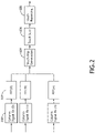
- the individual column signals received (Step 200) are deconstructed to provide the complete set of the FFT results (Step 202), which are then used to generate a touch map including the status of each of the nodes (Step 204).
- the mapping records the magnitude of the frequency of interest at each of the nodes. The magnitude can be thresholded against a running average for each node to normalize the data, for further processing, for instance to account for capacitance differences across the touch sensor array.
- the normalized mapping may then be input into more standardized touch detection algorithms, which may include multiple passes through the data to isolate touch positions and interpolate an accurate position (Step 206). Final touch positions are then reported to the higher-level system (Step 208).
- each column conductor of the touch sensor is measured over a predetermined period of time using an analog to digital converter (i.e., digitized).
- the sample set is then analyzed using the FFT algorithm and the FFT results are used to analyze the relative magnitude of the row conductor frequencies transmitted on each column conductor. A change in magnitude of one of the row frequencies indicates a touch on the row/column node.
- a change in the magnitude of a signal frequency of interest is used to determine the presence of a touch event (e.g., screen contact or close proximity gesture), as an object (e.g., finger, stylus, gloved finger, etc.) near a node will introduce an additional capacitance to the touch screen thereby decreasing the magnitude of the signal frequency coupled from a row to a column, and the location of the touch can be determined by analyzing the change in magnitude of the frequency of interest in the deconstructed column signal to determine in which corresponding row the touch occurred.
- a touch event e.g., screen contact or close proximity gesture
- each scan by the touch controller may include an output of the frequency set, receipt of the column signals, and deconstruction of the received column signals to identify a change in magnitude in one or more of the row frequencies of interest.
- Scans may occur periodically according to a predetermined scan rate, for example, approximately every 5 milliseconds such that a single touch will show on multiple successive scans.
- Touch points are detected by finding magnitude differences exceeding a predetermined threshold value and/or relative to neighboring node values (e.g., vertically, horizontally, and in some cases diagonally adjacent node neighbors).
- Additional system functionality may include more advanced touch event recognition algorithms such as object tracking over time by comparing successive scans or scan sets.
- the row conductor frequencies may be changed periodically so that a single EMI frequency is not able to affect a single row conductor.
- Such functionality may be implemented by rotating the row conductor that each unique frequency sine wave is transmitted on. For example, on the initial scan, FO may be transmitted on Row 0, on the second scan F0 may be transmitted on Row 1, and so on for each scan.
- FO may be transmitted on Row 0
- FO may be transmitted on Row 1
- any external signal frequency noise source will not interfere with the operation of the touch sensor.
- the number of signal frequencies in the signal set may correspond directly with the number of row conductors, e.g., 10 rows and 10 signal frequencies. In other embodiments, the number of signal frequencies may exceed the number of row conductors, e.g., 10 rows and 20 frequencies to increase the margin of EMI immunity.
- the touch controller 104 can be implemented in different touch sensitive display systems generally including a processor, a memory connected to the processor, a display, and a touch sensor applied to the display, for instance in an aircraft avionics display.
- two touch controllers can operate on sensor conductors in close proximity without interference by carefully choosing two separate frequency sets.
- redundant touch displays can be achieved as described further below.
- an exemplary embodiment of a display is shown at 400 including two separate functioning halves 302a, 302b.
- Each half includes a dedicated touch sensor 304a, 304b driven by its own dedicated touch controller 306a, 306b.
- the two halves operate separately, such that if one half fails the other remains operational.
- a touch sensor including a break in the middle of the row conductors could be used to achieve similar redundancy on the touch sensor side.
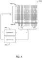
- an exemplary embodiment of another display is shown at 400 which includes interleaved conductors.
- every other row conductor and every other column conductor is driven and sensed by two separate touch controllers.
- every other row conductor 402a and every other column conductor 404a is driven by a first touch controller 406a
- every other row conductor 402b and every other column conductor 404b is driven by a second touch controller 406b.
- Each controller outputs a separate and distinct frequency set to its respective row conductors, and likewise receives column signals from its respective column electrodes.
- the touch sensor may have a standard pitch node pattern (e.g., diamond pattern) wherein in the case of single touch controller failure the resolution would decrease but the touch sensor would still operate.
- failure information could be shared with the graphic drawing application and only use areas of the display with good touch sensitivity.
- the touch sensor pattern could use smaller pitch nodes where the number of row and column conductors for the same size display is doubled, effectively doubling the resolution when both sensors are operational and in case of a single controller failure, the resolution would remain close to that of a standard pitch node pattern.
- Other configurations of interleaved row and column conductors are possible and envisioned.
- two individual controllers may each operate to input their unique frequency set to the same row conductors (R1, R2, R3..Rn).
- the two sinusoids one from the first controller (C1) and one from the second controller (C2), are added together and are output to the same row conductor (e.g., R1).
- Each column (L1, L2..Ln) of the sensor branches into two branches with each branch connected to one of the first controller (C1) and the second controller (C2).
- a 100-column sensor may include 100 column connections connected to the sensor inputs of the first controller (C1) and 100 column connections connected to the sensor inputs of the second controller (C2).
- the touch detection methodologies and hardware for implementing the same provides improved EMI immunity as compared to currently available capacitive touch systems.
- the touch detection methodologies further allow for a higher full screen scan rate, thereby reducing touch detection latency, allowing for multiple scans to further verify a touch event and validation while also allowing for redundant operation architectures.
Landscapes
- Engineering & Computer Science (AREA)
- General Engineering & Computer Science (AREA)
- Theoretical Computer Science (AREA)
- Human Computer Interaction (AREA)
- Physics & Mathematics (AREA)
- General Physics & Mathematics (AREA)
- Computer Networks & Wireless Communication (AREA)
- Position Input By Displaying (AREA)
Applications Claiming Priority (1)
| Application Number | Priority Date | Filing Date | Title |
|---|---|---|---|
| US17/131,371 US20220197436A1 (en) | 2020-12-22 | 2020-12-22 | Frequency analysis method of touch detection for projected capacitive touchscreens |
Publications (1)
| Publication Number | Publication Date |
|---|---|
| EP4020146A1 true EP4020146A1 (fr) | 2022-06-29 |
Family
ID=78821143
Family Applications (1)
| Application Number | Title | Priority Date | Filing Date |
|---|---|---|---|
| EP21211887.1A Withdrawn EP4020146A1 (fr) | 2020-12-22 | 2021-12-02 | Procédé d'analyse de fréquence de détection tactile pour écrans tactiles capacitifs projetés |
Country Status (2)
| Country | Link |
|---|---|
| US (1) | US20220197436A1 (fr) |
| EP (1) | EP4020146A1 (fr) |
Families Citing this family (2)
| Publication number | Priority date | Publication date | Assignee | Title |
|---|---|---|---|---|
| WO2022212920A1 (fr) * | 2021-04-01 | 2022-10-06 | Giant.Ai, Inc. | Architecture analogique et numérique combinée pour la gestion de données d'entrée sensorielles |
| TWI812973B (zh) * | 2021-07-02 | 2023-08-21 | 矽統科技股份有限公司 | 觸控系統及其感測方法與主動筆 |
Citations (4)
| Publication number | Priority date | Publication date | Assignee | Title |
|---|---|---|---|---|
| EP2264576A1 (fr) * | 2009-06-18 | 2010-12-22 | Wacom Co., Ltd. | Appareil de détection de pointeur et procédé de détection de pointeur |
| US20140152621A1 (en) * | 2011-11-11 | 2014-06-05 | Panasonic Corporation | Touch-panel device |
| US20160188085A1 (en) * | 2014-12-08 | 2016-06-30 | Tactual Labs Co. | Differential transmission for reduction of cross-talk in projective capacitive touch sensors |
| US20160224164A1 (en) * | 2012-08-23 | 2016-08-04 | Shanghai Tianma Micro-electronics Co., Ltd. | Mutual Capacitive Touch Panel |
Family Cites Families (5)
| Publication number | Priority date | Publication date | Assignee | Title |
|---|---|---|---|---|
| US9753586B2 (en) * | 2009-10-08 | 2017-09-05 | 3M Innovative Properties Company | Multi-touch touch device with multiple drive frequencies and maximum likelihood estimation |
| WO2015166898A1 (fr) * | 2014-04-28 | 2015-11-05 | シャープ株式会社 | Dispositif d'entrée et dispositif d'affichage |
| US20160231854A1 (en) * | 2015-02-06 | 2016-08-11 | Qualcomm Technologies, Inc. | Orthogonal frequency division scanning method for sensors |
| JP6309055B2 (ja) * | 2016-09-02 | 2018-04-11 | Nissha株式会社 | 抵抗膜式タッチパネルからのデータ取得方法、及び抵抗膜式タッチパネル装置 |
| US10503312B2 (en) * | 2018-01-18 | 2019-12-10 | Elo Touch Solutions, Inc. | Large PCAP screen with multiple touch controller ASICS with interleaved receiver connections |
-
2020
- 2020-12-22 US US17/131,371 patent/US20220197436A1/en not_active Abandoned
-
2021
- 2021-12-02 EP EP21211887.1A patent/EP4020146A1/fr not_active Withdrawn
Patent Citations (4)
| Publication number | Priority date | Publication date | Assignee | Title |
|---|---|---|---|---|
| EP2264576A1 (fr) * | 2009-06-18 | 2010-12-22 | Wacom Co., Ltd. | Appareil de détection de pointeur et procédé de détection de pointeur |
| US20140152621A1 (en) * | 2011-11-11 | 2014-06-05 | Panasonic Corporation | Touch-panel device |
| US20160224164A1 (en) * | 2012-08-23 | 2016-08-04 | Shanghai Tianma Micro-electronics Co., Ltd. | Mutual Capacitive Touch Panel |
| US20160188085A1 (en) * | 2014-12-08 | 2016-06-30 | Tactual Labs Co. | Differential transmission for reduction of cross-talk in projective capacitive touch sensors |
Also Published As
| Publication number | Publication date |
|---|---|
| US20220197436A1 (en) | 2022-06-23 |
Similar Documents
| Publication | Publication Date | Title |
|---|---|---|
| US9760192B2 (en) | Touch sensing | |
| US9753586B2 (en) | Multi-touch touch device with multiple drive frequencies and maximum likelihood estimation | |
| TWI501122B (zh) | 用以辨識在多接觸同時輸入指示的實際接觸點之方法及多接觸輸入裝置 | |
| EP3144790B1 (fr) | Panneau et circuit de détection tactiles | |
| US8232970B2 (en) | Scan sequence generator | |
| US20110181519A1 (en) | System and method of driving a touch screen | |
| US20130050132A1 (en) | Techniques for capacitive touch screen control | |
| JP5801638B2 (ja) | タッチパネル | |
| US20160195993A1 (en) | Multi-touch detection | |
| US20130106759A1 (en) | Narrow-Band Touch Detection | |
| US9606670B2 (en) | Real-time spectral noise monitoring for proximity sensing device | |
| EP3190485B1 (fr) | Panneau tactile capacitif | |
| WO2012075191A1 (fr) | Détecteur de capacitance à couche simple projetée linéaire | |
| JP2013004102A (ja) | 多周波の容量検出を伴うマルチタッチのタッチセンサー式装置 | |
| CN104641325B (zh) | 触摸感应显示器的改进 | |
| EP4020146A1 (fr) | Procédé d'analyse de fréquence de détection tactile pour écrans tactiles capacitifs projetés | |
| US10216322B2 (en) | Capacitive touch sense unit computation power reduction using keypad electrodes crosstalk | |
| EP2853999B1 (fr) | Panneau tactile capacitif | |
| GB2584669A (en) | Touch-sensitive apparatus and method | |
| EP4428663B1 (fr) | Détection de localisation de panneau tactile avec différentes combinaisons de décalage de phase de fréquence de signaux d'électrode | |
| US20190317656A1 (en) | Drive line allocation | |
| US11635851B2 (en) | Sensor filter for calibrating a touch system | |
| GB2623544A (en) | Touch-sensitive apparatus and method | |
| GB2607596A (en) | Touch-sensitive apparatus and method |
Legal Events
| Date | Code | Title | Description |
|---|---|---|---|
| PUAI | Public reference made under article 153(3) epc to a published international application that has entered the european phase |
Free format text: ORIGINAL CODE: 0009012 |
|
| STAA | Information on the status of an ep patent application or granted ep patent |
Free format text: STATUS: THE APPLICATION HAS BEEN PUBLISHED |
|
| AK | Designated contracting states |
Kind code of ref document: A1 Designated state(s): AL AT BE BG CH CY CZ DE DK EE ES FI FR GB GR HR HU IE IS IT LI LT LU LV MC MK MT NL NO PL PT RO RS SE SI SK SM TR |
|
| STAA | Information on the status of an ep patent application or granted ep patent |
Free format text: STATUS: REQUEST FOR EXAMINATION WAS MADE |
|
| 17P | Request for examination filed |
Effective date: 20221228 |
|
| RBV | Designated contracting states (corrected) |
Designated state(s): AL AT BE BG CH CY CZ DE DK EE ES FI FR GB GR HR HU IE IS IT LI LT LU LV MC MK MT NL NO PL PT RO RS SE SI SK SM TR |
|
| STAA | Information on the status of an ep patent application or granted ep patent |
Free format text: STATUS: EXAMINATION IS IN PROGRESS |
|
| 17Q | First examination report despatched |
Effective date: 20231204 |
|
| STAA | Information on the status of an ep patent application or granted ep patent |
Free format text: STATUS: THE APPLICATION HAS BEEN WITHDRAWN |
|
| 18W | Application withdrawn |
Effective date: 20240403 |