EP4020227B1 - Dynamische gemeinsame cache-partition für arbeitslast mit grossem code-fussabdruck - Google Patents
Dynamische gemeinsame cache-partition für arbeitslast mit grossem code-fussabdruck Download PDFInfo
- Publication number
- EP4020227B1 EP4020227B1 EP21196229.5A EP21196229A EP4020227B1 EP 4020227 B1 EP4020227 B1 EP 4020227B1 EP 21196229 A EP21196229 A EP 21196229A EP 4020227 B1 EP4020227 B1 EP 4020227B1
- Authority
- EP
- European Patent Office
- Prior art keywords
- cache
- code
- workload
- ways
- level
- Prior art date
- Legal status (The legal status is an assumption and is not a legal conclusion. Google has not performed a legal analysis and makes no representation as to the accuracy of the status listed.)
- Active
Links
Images








Classifications
-
- G—PHYSICS
- G06—COMPUTING OR CALCULATING; COUNTING
- G06F—ELECTRIC DIGITAL DATA PROCESSING
- G06F12/00—Accessing, addressing or allocating within memory systems or architectures
- G06F12/02—Addressing or allocation; Relocation
- G06F12/08—Addressing or allocation; Relocation in hierarchically structured memory systems, e.g. virtual memory systems
- G06F12/0802—Addressing of a memory level in which the access to the desired data or data block requires associative addressing means, e.g. caches
- G06F12/0806—Multiuser, multiprocessor or multiprocessing cache systems
- G06F12/084—Multiuser, multiprocessor or multiprocessing cache systems with a shared cache
-
- G—PHYSICS
- G06—COMPUTING OR CALCULATING; COUNTING
- G06F—ELECTRIC DIGITAL DATA PROCESSING
- G06F12/00—Accessing, addressing or allocating within memory systems or architectures
- G06F12/02—Addressing or allocation; Relocation
- G06F12/08—Addressing or allocation; Relocation in hierarchically structured memory systems, e.g. virtual memory systems
- G06F12/0802—Addressing of a memory level in which the access to the desired data or data block requires associative addressing means, e.g. caches
- G06F12/0806—Multiuser, multiprocessor or multiprocessing cache systems
- G06F12/0811—Multiuser, multiprocessor or multiprocessing cache systems with multilevel cache hierarchies
-
- G—PHYSICS
- G06—COMPUTING OR CALCULATING; COUNTING
- G06F—ELECTRIC DIGITAL DATA PROCESSING
- G06F12/00—Accessing, addressing or allocating within memory systems or architectures
- G06F12/02—Addressing or allocation; Relocation
- G06F12/08—Addressing or allocation; Relocation in hierarchically structured memory systems, e.g. virtual memory systems
- G06F12/0802—Addressing of a memory level in which the access to the desired data or data block requires associative addressing means, e.g. caches
- G06F12/0844—Multiple simultaneous or quasi-simultaneous cache accessing
- G06F12/0846—Cache with multiple tag or data arrays being simultaneously accessible
- G06F12/0848—Partitioned cache, e.g. separate instruction and operand caches
-
- G—PHYSICS
- G06—COMPUTING OR CALCULATING; COUNTING
- G06F—ELECTRIC DIGITAL DATA PROCESSING
- G06F12/00—Accessing, addressing or allocating within memory systems or architectures
- G06F12/02—Addressing or allocation; Relocation
- G06F12/08—Addressing or allocation; Relocation in hierarchically structured memory systems, e.g. virtual memory systems
- G06F12/0802—Addressing of a memory level in which the access to the desired data or data block requires associative addressing means, e.g. caches
- G06F12/0866—Addressing of a memory level in which the access to the desired data or data block requires associative addressing means, e.g. caches for peripheral storage systems, e.g. disk cache
- G06F12/0871—Allocation or management of cache space
-
- G—PHYSICS
- G06—COMPUTING OR CALCULATING; COUNTING
- G06F—ELECTRIC DIGITAL DATA PROCESSING
- G06F12/00—Accessing, addressing or allocating within memory systems or architectures
- G06F12/02—Addressing or allocation; Relocation
- G06F12/08—Addressing or allocation; Relocation in hierarchically structured memory systems, e.g. virtual memory systems
- G06F12/0802—Addressing of a memory level in which the access to the desired data or data block requires associative addressing means, e.g. caches
- G06F12/0893—Caches characterised by their organisation or structure
- G06F12/0895—Caches characterised by their organisation or structure of parts of caches, e.g. directory or tag array
-
- G—PHYSICS
- G06—COMPUTING OR CALCULATING; COUNTING
- G06F—ELECTRIC DIGITAL DATA PROCESSING
- G06F9/00—Arrangements for program control, e.g. control units
- G06F9/06—Arrangements for program control, e.g. control units using stored programs, i.e. using an internal store of processing equipment to receive or retain programs
- G06F9/46—Multiprogramming arrangements
- G06F9/50—Allocation of resources, e.g. of the central processing unit [CPU]
- G06F9/5005—Allocation of resources, e.g. of the central processing unit [CPU] to service a request
- G06F9/5011—Allocation of resources, e.g. of the central processing unit [CPU] to service a request the resources being hardware resources other than CPUs, Servers and Terminals
- G06F9/5016—Allocation of resources, e.g. of the central processing unit [CPU] to service a request the resources being hardware resources other than CPUs, Servers and Terminals the resource being the memory
Definitions
- This disclosure generally relates to processor technology, processor cache technology, and cache controller technology.
- code and data caches closest to the processor may be referred to as first level (L1) caches (e.g., a L1 code cache and a L1 data cache).
- the next level caches e.g., a second level (L2) cache, a third level cache (L3), etc.
- LLC mid-level cache
- a last level cache (LLC) may refer to a highest-level cache that may be shared by functional units in the same chip/package with the LLC.
- US2012054442 discloses partitioning an unified cache into a first portion of lines that only store copies of instructions retrieved from a memory and a second portion of lines that only store copies of data retrieved from the memory.
- US6532520 discloses allocating data and instructions within a shared cache.
- Embodiments discussed herein variously provide techniques and mechanisms for controlling a cache.
- the technologies described herein may be implemented in one or more electronic devices.
- electronic devices that may utilize the technologies described herein include any kind of mobile device and/or stationary device, such as cameras, cell phones, computer terminals, desktop computers, electronic readers, facsimile machines, kiosks, laptop computers, netbook computers, notebook computers, internet devices, payment terminals, personal digital assistants, media players and/or recorders, servers (e.g., blade server, rack mount server, combinations thereof, etc.), set-top boxes, smart phones, tablet personal computers, ultra-mobile personal computers, wired telephones, combinations thereof, and the like. More generally, the technologies described herein may be employed in any of a variety of electronic devices including integrated circuitry which is operable to control or utilize a cache.
- signals are represented with lines. Some lines may be thicker, to indicate a greater number of constituent signal paths, and/or have arrows at one or more ends, to indicate a direction of information flow. Such indications are not intended to be limiting. Rather, the lines are used in connection with one or more exemplary embodiments to facilitate easier understanding of a circuit or a logical unit. Any represented signal, as dictated by design needs or preferences, may actually comprise one or more signals that may travel in either direction and may be implemented with any suitable type of signal scheme.
- connection means a direct connection, such as electrical, mechanical, or magnetic connection between the things that are connected, without any intermediary devices.
- coupled means a direct or indirect connection, such as a direct electrical, mechanical, or magnetic connection between the things that are connected or an indirect connection, through one or more passive or active intermediary devices.
- circuit or “module” may refer to one or more passive and/or active components that are arranged to cooperate with one another to provide a desired function.
- signal may refer to at least one current signal, voltage signal, magnetic signal, or data/clock signal.
- the meaning of "a,” “an,” and “the” include plural references.
- the meaning of "in” includes “in” and "on.”
- scaling generally refers to converting a design (schematic and layout) from one process technology to another process technology and subsequently being reduced in layout area.
- scaling generally also refers to downsizing layout and devices within the same technology node.
- scaling may also refer to adjusting (e.g., slowing down or speeding up - i.e. scaling down, or scaling up respectively) of a signal frequency relative to another parameter, for example, power supply level.
- the terms “substantially,” “close,” “approximately,” “near,” and “about,” generally refer to being within +/- 10% of a target value.
- the terms “substantially equal,” “about equal” and “approximately equal” mean that there is no more than incidental variation between among things so described. In the art, such variation is typically no more than +/-10% of a predetermined target value.
- a first material "over" a second material in the context of a figure provided herein may also be "under” the second material if the device is oriented upside-down relative to the context of the figure provided.
- one material disposed over or under another may be directly in contact or may have one or more intervening materials.
- one material disposed between two materials may be directly in contact with the two layers or may have one or more intervening layers.
- a first material "on" a second material is in direct contact with that second material. Similar distinctions are to be made in the context of component assemblies.
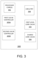
- an embodiment of an integrated circuit 100 may include a core 111, a first level core cache memory 112 coupled to the core 111, a shared core cache memory 113 coupled to the core 111, a first cache controller 114a coupled to the core 111 and communicatively coupled to the first level core cache memory 112, a second cache controller 114b coupled to the core 111 and communicatively coupled to the shared core cache memory 113, and circuitry 115 coupled to the core 111 and communicatively coupled to the first cache controller 114a and the second cache controller 114b to determine if a workload has a large code footprint, and, if so determined, partition N ways of the shared core cache memory 113 into first and second chunks of ways with the first chunk of M ways reserved for code cache lines from the workload and the second chunk of N minus M ways reserved for data cache lines from the workload, where N and M are positive integer values and N minus M is greater than zero.
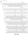
- Some embodiments of the method 200 may further include restricting code cache lines from the workload to occupy the first chunk of ways for code for the workload at box 230, and restricting data cache lines from the workload to occupy the second chunk of ways for data for the workload at box 231.
- the method 200 may also include decreasing priority of non-hit cache lines in only the first chunk of ways for code in response to a demand hit to a cache line in the first chunk of ways for code at box 232, and decreasing priority of non-hit cache lines in only the second chunk of ways for data in response to a demand hit to a cache line in the second chunk of ways for data at box 233.
- Processor cores may be implemented in different ways, for different purposes, and in different processors.
- implementations of such cores may include: 1) a general purpose in-order core intended for general-purpose computing; 2) a high performance general purpose out-of-order core intended for general-purpose computing; 3) a special purpose core intended primarily for graphics and/or scientific (throughput) computing.
- Implementations of different processors may include: 1) a CPU including one or more general purpose in-order cores intended for general-purpose computing and/or one or more general purpose out-of-order cores intended for general-purpose computing; and 2) a coprocessor including one or more special purpose cores intended primarily for graphics and/or scientific (throughput).
- Such different processors lead to different computer system architectures, which may include: 1) the coprocessor on a separate chip from the CPU; 2) the coprocessor on a separate die in the same package as a CPU; 3) the coprocessor on the same die as a CPU (in which case, such a coprocessor is sometimes referred to as special purpose logic, such as integrated graphics and/or scientific (throughput) logic, or as special purpose cores); and 4) a system on a chip that may include on the same die the described CPU (sometimes referred to as the application core(s) or application processor(s)), the above described coprocessor, and additional functionality.
- Exemplary core architectures are described next, followed by descriptions of exemplary processors and computer architectures.
- FIG. 6A is a block diagram illustrating both an exemplary in-order pipeline and an exemplary register renaming, out-of-order issue/execution pipeline according to embodiments of the invention.
- FIG. 6B is a block diagram illustrating both an exemplary embodiment of an in-order architecture core and an exemplary register renaming, out-of-order issue/execution architecture core to be included in a processor according to embodiments of the invention.
- the solid lined boxes in FIGs. 6A-B illustrate the in-order pipeline and in-order core, while the optional addition of the dashed lined boxes illustrates the register renaming, out-of-order issue/execution pipeline and core. Given that the in-order aspect is a subset of the out-of-order aspect, the out-of-order aspect will be described.
- a processor pipeline 900 includes a fetch stage 902, a length decode stage 904, a decode stage 906, an allocation stage 908, a renaming stage 910, a scheduling (also known as a dispatch or issue) stage 912, a register read/memory read stage 914, an execute stage 916, a write back/memory write stage 918, an exception handling stage 922, and a commit stage 924.
- FIG. 6B shows processor core 990 including a front end unit 930 coupled to an execution engine unit 950, and both are coupled to a memory unit 970.
- the core 990 may be a reduced instruction set computing (RISC) core, a complex instruction set computing (CISC) core, a very long instruction word (VLIW) core, or a hybrid or alternative core type.
- the core 990 may be a special-purpose core, such as, for example, a network or communication core, compression engine, coprocessor core, general purpose computing graphics processing unit (GPGPU) core, graphics core, or the like.
- GPGPU general purpose computing graphics processing unit
- the front end unit 930 includes a branch prediction unit 932 coupled to an instruction cache unit 934, which is coupled to an instruction translation lookaside buffer (TLB) 936, which is coupled to an instruction fetch unit 938, which is coupled to a decode unit 940.
- the decode unit 940 (or decoder) may decode instructions, and generate as an output one or more micro-operations, micro-code entry points, microinstructions, other instructions, or other control signals, which are decoded from, or which otherwise reflect, or are derived from, the original instructions.
- the decode unit 940 may be implemented using various different mechanisms.
- the core 990 includes a microcode ROM or other medium that stores microcode for certain macroinstructions (e.g., in decode unit 940 or otherwise within the front end unit 930).
- the decode unit 940 is coupled to a rename/allocator unit 952 in the execution engine unit 950.
- the execution engine unit 950 includes the rename/allocator unit 952 coupled to a retirement unit 954 and a set of one or more scheduler unit(s) 956.
- the scheduler unit(s) 956 represents any number of different schedulers, including reservations stations, central instruction window, etc.
- the scheduler unit(s) 956 is coupled to the physical register file(s) unit(s) 958.
- Each of the physical register file(s) units 958 represents one or more physical register files, different ones of which store one or more different data types, such as scalar integer, scalar floating point, packed integer, packed floating point, vector integer, vector floating point, status (e.g., an instruction pointer that is the address of the next instruction to be executed), etc.
- the physical register file(s) unit 958 comprises a vector registers unit, a write mask registers unit, and a scalar registers unit. These register units may provide architectural vector registers, vector mask registers, and general purpose registers.
- the physical register file(s) unit(s) 958 is overlapped by the retirement unit 954 to illustrate various ways in which register renaming and out-of-order execution may be implemented (e.g., using a reorder buffer(s) and a retirement register file(s); using a future file(s), a history buffer(s), and a retirement register file(s); using a register maps and a pool of registers; etc.).
- the retirement unit 954 and the physical register file(s) unit(s) 958 are coupled to the execution cluster(s) 960.
- the execution cluster(s) 960 includes a set of one or more execution units 962 and a set of one or more memory access units 964.
- the execution units 962 may perform various operations (e.g., shifts, addition, subtraction, multiplication) and on various types of data (e.g., scalar floating point, packed integer, packed floating point, vector integer, vector floating point). While some embodiments may include a number of execution units dedicated to specific functions or sets of functions, other embodiments may include only one execution unit or multiple execution units that all perform all functions.
- the scheduler unit(s) 956, physical register file(s) unit(s) 958, and execution cluster(s) 960 are shown as being possibly plural because certain embodiments create separate pipelines for certain types of data/operations (e.g., a scalar integer pipeline, a scalar floating point/packed integer/packed floating point/vector integer/vector floating point pipeline, and/or a memory access pipeline that each have their own scheduler unit, physical register file(s) unit, and/or execution cluster - and in the case of a separate memory access pipeline, certain embodiments are implemented in which only the execution cluster of this pipeline has the memory access unit(s) 964). It should also be understood that where separate pipelines are used, one or more of these pipelines may be out-of-order issue/execution and the rest in-order.
- the set of memory access units 964 is coupled to the memory unit 970, which includes a data TLB unit 972 coupled to a data cache unit 974 coupled to a level 2 (L2) cache unit 976.
- the memory access units 964 may include a load unit, a store address unit, and a store data unit, each of which is coupled to the data TLB unit 972 in the memory unit 970.
- the instruction cache unit 934 is further coupled to a level 2 (L2) cache unit 976 in the memory unit 970.
- the L2 cache unit 976 is coupled to one or more other levels of cache and eventually to a main memory.
- the exemplary register renaming, out-of-order issue/execution core architecture may implement the pipeline 900 as follows: 1) the instruction fetch 938 performs the fetch and length decoding stages 902 and 904; 2) the decode unit 940 performs the decode stage 906; 3) the rename/allocator unit 952 performs the allocation stage 908 and renaming stage 910; 4) the scheduler unit(s) 956 performs the schedule stage 912; 5) the physical register file(s) unit(s) 958 and the memory unit 970 perform the register read/memory read stage 914; the execution cluster 960 perform the execute stage 916; 6) the memory unit 970 and the physical register file(s) unit(s) 958 perform the write back/memory write stage 918; 7) various units may be involved in the exception handling stage 922; and 8) the retirement unit 954 and the physical register file(s) unit(s) 958 perform the commit stage 924.
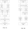
- FIG. 7B is an expanded view of part of the processor core in FIG. 7A according to embodiments of the invention.
- FIG. 7B includes an L1 data cache 1006A part of the L1 cache 1006, as well as more detail regarding the vector unit 1010 and the vector registers 1014.
- the vector unit 1010 is a 16-wide vector processing unit (VPU) (see the 16-wide ALU 1028), which executes one or more of integer, single-precision float, and double-precision float instructions.
- the VPU supports swizzling the register inputs with swizzle unit 1020, numeric conversion with numeric convert units 1022A-B, and replication with replication unit 1024 on the memory input.
- Write mask registers 1026 allow predicating resulting vector writes.
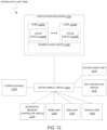
- various I/O devices 1314 may be coupled to first bus 1316, along with a bus bridge 1318 which couples first bus 1316 to a second bus 1320.
- one or more additional processor(s) 1315 such as coprocessors, high-throughput MIC processors, GPGPU's, accelerators (such as, e.g., graphics accelerators or digital signal processing (DSP) units), field programmable gate arrays, or any other processor, are coupled to first bus 1316.
- second bus 1320 may be a low pin count (LPC) bus.
- Embodiments of the mechanisms disclosed herein may be implemented in hardware, software, firmware, or a combination of such implementation approaches.
- Embodiments of the invention may be implemented as computer programs or program code executing on programmable systems comprising at least one processor, a storage system (including volatile and non-volatile memory and/or storage elements), at least one input device, and at least one output device.
- Program code such as code 1330 illustrated in FIG. 10
- Program code 1330 illustrated in FIG. 10 may be applied to input instructions to perform the functions described herein and generate output information.
- the output information may be applied to one or more output devices, in known fashion.
- a processing system includes any system that has a processor, such as, for example; a digital signal processor (DSP), a microcontroller, an application specific integrated circuit (ASIC), or a microprocessor.
- DSP digital signal processor
- ASIC application specific integrated circuit
- IP cores may be stored on a tangible, machine readable medium and supplied to various customers or manufacturing facilities to load into the fabrication machines that actually make the logic or processor.
- embodiments of the invention also include non-transitory, tangible machine-readable media containing instructions or containing design data, such as Hardware Description Language (HDL), which defines structures, circuits, apparatuses, processors and/or system features described herein.
- HDL Hardware Description Language
- Such embodiments may also be referred to as program products.
- Emulation including binary translation, code morphing, etc.
- an instruction converter may be used to convert an instruction from a source instruction set to a target instruction set.
- the instruction converter may translate (e.g., using static binary translation, dynamic binary translation including dynamic compilation), morph, emulate, or otherwise convert an instruction to one or more other instructions to be processed by the core.
- the instruction converter may be implemented in software, hardware, firmware, or a combination thereof.
- the instruction converter may be on processor, off processor, or part on and part off processor.
- FIG. 13 is a block diagram contrasting the use of a software instruction converter to convert binary instructions in a source instruction set to binary instructions in a target instruction set according to embodiments of the invention.
- the instruction converter is a software instruction converter, although alternatively the instruction converter may be implemented in software, firmware, hardware, or various combinations thereof.
- FIG. 13 shows a program in a high level language 1602 may be compiled using an x86 compiler 1604 to generate x86 binary code 1606 that may be natively executed by a processor with at least one x86 instruction set core 1616.
Landscapes
- Engineering & Computer Science (AREA)
- Theoretical Computer Science (AREA)
- Physics & Mathematics (AREA)
- General Engineering & Computer Science (AREA)
- General Physics & Mathematics (AREA)
- Software Systems (AREA)
- Memory System Of A Hierarchy Structure (AREA)
Claims (8)
- Integrierte Schaltung, die Folgendes umfasst:einen Kern (111);einen Kern-Cache-Speicher (112) erster Ebene, der mit dem Kern (111) gekoppelt ist;einen gemeinsam genutzten Kern-Cache-Speicher (113), der mit dem Kern (111) gekoppelt ist;eine erste Cache-Steuerung (114a), die mit dem Kern (111) gekoppelt ist und kommunikativ mit dem Kern-Cache-Speicher (112) erster Ebene gekoppelt ist;eine zweite Cache-Steuerung (114b), die mit dem Kern (111) gekoppelt ist und kommunikativ mit dem gemeinsam genutzten Kern-Cache-Speicher (113) gekoppelt ist; undeine Schaltungsanordnung (115), die mit dem Kern (111) gekoppelt ist und kommunikativ mit der ersten Cache-Steuerung (113) und der zweiten Cache-Steuerung (114b) gekoppelt ist, um Folgendes durchzuführen:Bestimmen, ob eine Arbeitslast einen großen Code-Fußabdruck hat, basierend auf einer Anzahl von Code-Cache-Fehlversuchen der ersten Ebene von der Arbeitslast und einer Anzahl von Daten-Cache-Fehlversuchen der ersten Ebene von der Arbeitslast, und, falls so bestimmt,Partitionieren von N Wegen des gemeinsam genutzten Kern-Cache-Speichers (113) in erste und zweite Blöcke von Wegen, wobei der erste Block von M Wegen für Code-Cache-Zeilen von der Arbeitslast reserviert ist und der zweite Block von N minus M Wegen für Daten-Cache-Zeilen von der Arbeitslast reserviert ist, wobei N und M positive ganzzahlige Werte sind und N minus M größer als Null ist, dadurch gekennzeichnet, dass:
das Bestimmen, ob eine Arbeitslast einen großen Code-Fußabdruck aufweist, Folgendes umfasst:Zählen der Anzahl der Code-Cache-Fehlversuche der ersten Ebene von der Arbeitslast;Zählen der Anzahl der Daten-Cache-Fehlversuche der ersten Ebene von der Arbeitslast; undBestimmen, dass die Arbeitslast den großen Code-Fußabdruck hat, wenn die gezählte Anzahl von Code-Cache-Fehlversuchen der ersten Ebene die gezählte Anzahl von Daten-Cache-Fehlversuchen der ersten Ebene übersteigt,nachdem eine gezählte Anzahl von Cache-Fehlversuchen der ersten Ebene einen Schwellenwert überschreitet. - Integrierte Schaltung nach Anspruch 1, wobei die Schaltung ferner für Folgendes ausgebildet ist:Zurücksetzen der Anzahl von Code-Cache-Fehlversuchen der ersten Ebene auf die Hälfte der gezählten Anzahl von Code-Cache-Fehlversuchen der ersten Ebene, nachdem die gezählte Anzahl von Cache-Fehlversuchen der ersten Ebene den Schwellenwert überschritten hat;Zurücksetzen der Anzahl von Daten-Cache-Fehlversuchen der ersten Ebene auf die Hälfte der gezählten Anzahl von Daten-Cache-Fehlversuchen der ersten Ebene, nachdem die gezählte Anzahl von Cache-Fehlversuchen der ersten Ebene den Schwellenwert überschritten hat; undZurücksetzen der Anzahl der Cache-Fehlversuche der ersten Ebene auf Null, nachdem die gezählte Anzahl der Cache-Fehlversuche der ersten Ebene den Schwellenwert überschritten hat.
- Integrierte Schaltung nach einem der Ansprüche 1 bis 2, wobei die Schaltung ferner für Folgendes ausgebildet ist:Beschränken von Code-Cache-Zeilen aus der Arbeitslast, um den ersten Block von Wegen für Code für die Arbeitslast zu belegen; undBeschränken der Daten-Cache-Zeilen aus der Arbeitslast, um den zweiten Block von Wegen für Daten für die Arbeitslast zu belegen.
- Verfahren (200) zur Steuerung eines Caches, das Folgendes umfasst:Bestimmen (221), ob eine Arbeitslast einen großen Code-Fußabdruck hat, basierend auf einer Anzahl von Code-Cache-Fehlversuchen der ersten Ebene von der Arbeitslast und einer Anzahl von Daten-Cache-Fehlversuchen der ersten Ebene von der Arbeitslast; und, falls so bestimmt,Partitionieren (222) von N Wegen des gemeinsam genutzten Kern-Cache-Speichers in erste und zweite Blöcke von Wegen, wobei der erste Block von M Wegen für Code-Cache-Zeilen von der Arbeitslast reserviert ist und der zweite Block von N minus M Wegen für Daten-Cache-Zeilen von der Arbeitslast reserviert ist, wobei N und M positive ganzzahlige Werte sind und N minus M größer als Null ist, dadurch gekennzeichnet, dass:
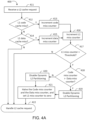
wobei das Bestimmen, ob eine Arbeitslast einen großen Code-Fußabdruck hat, Folgendes umfasst:Zählen der Anzahl der Code-Cache-Fehlversuche der ersten Ebene durch die Arbeitslast;Zählen der Anzahl der Daten-Cache-Fehlversuche der ersten Ebene durch die Arbeitslast;und Bestimmen, dass die Arbeitslast den großen Code-Fußabdruck hat, wenn die gezählte Anzahl von Code-Cache-Fehlversuchen der ersten Ebene die gezählte Anzahl von Daten-Cache-Fehlversuchen der ersten Ebene übersteigt, nachdem eine gezählte Anzahl von Cache-Fehlversuchen der ersten Ebene einen Schwellenwert überschreitet. - Verfahren (200) nach Anspruch 4, das ferner Folgendes umfasst:Beschränken (230) von Code-Cache-Zeilen aus der Arbeitslast, um den ersten Block von Wegen für Code für die Arbeitslast zu belegen; undBeschränken (231) von Daten-Cache-Zeilen aus der Arbeitslast, um den zweiten Block von Wegen für Daten für die Arbeitslast zu belegen.
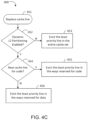
- Verfahren nach Anspruch 5, das ferner Folgendes umfasst:Verringern der Priorität von Nicht-Treffer-Cache-Zeilen nur in dem ersten Block von Wegen für Code als Reaktion auf einen Bedarfstreffer auf eine Cache-Zeile in dem ersten Block von Wegen für Code; undVerringern der Priorität von Nicht-Treffer-Cache-Zeilen nur in dem zweiten Block von Wegen für Daten als Reaktion auf eine Anforderung, die auf eine Cache-Zeile in dem zweiten Block von Wegen für Daten trifft.
- Verfahren nach einem der Ansprüche 5 bis 6, das ferner Folgendes umfasst:Entfernen einer Cache-Zeile mit der niedrigsten Priorität nur aus dem ersten Block von Wegen für Code, um eine Code-Cache-Zeile in den ersten Block von Wegen für Code einzufügen; undEntfernen einer Cache-Zeile mit der niedrigsten Priorität nur aus dem zweiten Block von Wegen für Daten, um eine Daten-Cache-Zeile in den zweiten Block von Wegen für Daten einzufügen.
- Mindestens ein nichtflüchtiges computerlesbares Medium, das eine Vielzahl von Anweisungen umfasst, die als Reaktion auf die Ausführung auf einer Rechenvorrichtung die Rechenvorrichtung veranlassen, ein Verfahren nach einem der Ansprüche 4 bis 7 auszuführen.
Applications Claiming Priority (1)
| Application Number | Priority Date | Filing Date | Title |
|---|---|---|---|
| US17/130,698 US12066945B2 (en) | 2020-12-22 | 2020-12-22 | Dynamic shared cache partition for workload with large code footprint |
Publications (2)
| Publication Number | Publication Date |
|---|---|
| EP4020227A1 EP4020227A1 (de) | 2022-06-29 |
| EP4020227B1 true EP4020227B1 (de) | 2025-02-26 |
Family
ID=77738971
Family Applications (1)
| Application Number | Title | Priority Date | Filing Date |
|---|---|---|---|
| EP21196229.5A Active EP4020227B1 (de) | 2020-12-22 | 2021-09-13 | Dynamische gemeinsame cache-partition für arbeitslast mit grossem code-fussabdruck |
Country Status (4)
| Country | Link |
|---|---|
| US (1) | US12066945B2 (de) |
| EP (1) | EP4020227B1 (de) |
| CN (1) | CN114661629A (de) |
| TW (1) | TW202225978A (de) |
Families Citing this family (5)
| Publication number | Priority date | Publication date | Assignee | Title |
|---|---|---|---|---|
| US12182018B2 (en) | 2020-12-23 | 2024-12-31 | Intel Corporation | Instruction and micro-architecture support for decompression on core |
| US12242851B2 (en) | 2021-09-09 | 2025-03-04 | Intel Corporation | Verifying compressed stream fused with copy or transform operations |
| US12417182B2 (en) | 2021-12-14 | 2025-09-16 | Intel Corporation | De-prioritizing speculative code lines in on-chip caches |
| US12360768B2 (en) | 2021-12-16 | 2025-07-15 | Intel Corporation | Throttling code fetch for speculative code paths |
| CN115827547A (zh) * | 2022-11-16 | 2023-03-21 | 中山大学 | 一种多核处理器动态缓存分区隔离系统及其控制方法 |
Family Cites Families (5)
| Publication number | Priority date | Publication date | Assignee | Title |
|---|---|---|---|---|
| US6532520B1 (en) | 1999-09-10 | 2003-03-11 | International Business Machines Corporation | Method and apparatus for allocating data and instructions within a shared cache |
| US6378044B1 (en) * | 1999-09-22 | 2002-04-23 | Vlsi Technology, Inc. | Method and system for cache replacement among configurable cache sets |
| US8244981B2 (en) * | 2009-07-10 | 2012-08-14 | Apple Inc. | Combined transparent/non-transparent cache |
| US8909867B2 (en) | 2010-08-24 | 2014-12-09 | Advanced Micro Devices, Inc. | Method and apparatus for allocating instruction and data for a unified cache |
| US10642618B1 (en) * | 2016-06-02 | 2020-05-05 | Apple Inc. | Callgraph signature prefetch |
-
2020
- 2020-12-22 US US17/130,698 patent/US12066945B2/en active Active
-
2021
- 2021-09-09 TW TW110133608A patent/TW202225978A/zh unknown
- 2021-09-13 EP EP21196229.5A patent/EP4020227B1/de active Active
- 2021-11-22 CN CN202111388882.XA patent/CN114661629A/zh active Pending
Also Published As
| Publication number | Publication date |
|---|---|
| TW202225978A (zh) | 2022-07-01 |
| CN114661629A (zh) | 2022-06-24 |
| US12066945B2 (en) | 2024-08-20 |
| EP4020227A1 (de) | 2022-06-29 |
| US20220197794A1 (en) | 2022-06-23 |
Similar Documents
| Publication | Publication Date | Title |
|---|---|---|
| EP4020227B1 (de) | Dynamische gemeinsame cache-partition für arbeitslast mit grossem code-fussabdruck | |
| EP3394757B1 (de) | Hardware-vorrichtungen und verfahren zur erkennung von speicherkorruption | |
| US20230093247A1 (en) | Memory access tracker in device private memory | |
| US20240232096A9 (en) | Hardware assisted memory access tracking | |
| US12332802B2 (en) | Multi-stage cache tag with first stage tag size reduction | |
| US12153925B2 (en) | Alternate path decode for hard-to-predict branch | |
| WO2017172354A1 (en) | Hardware apparatuses and methods for memory performance monitoring | |
| US20140189192A1 (en) | Apparatus and method for a multiple page size translation lookaside buffer (tlb) | |
| EP4020229A1 (de) | System, vorrichtung und verfahren zum prefetching von physikalischen seiten in einem prozessor | |
| US11847053B2 (en) | Apparatuses, methods, and systems for a duplication resistant on-die irregular data prefetcher | |
| EP4002131B1 (de) | Sequestrierter speicher zur selektiven speicherung von metadaten entsprechend zwischengespeicherten daten | |
| US12449976B2 (en) | PASID granularity resource control for IOMMU | |
| US20220129763A1 (en) | High confidence multiple branch offset predictor | |
| US20220197798A1 (en) | Single re-use processor cache policy | |
| EP4020228B1 (de) | Vorrichtung, system und verfahren zum selektiven löschen von prefetch-befehlen für software | |
| US20230195634A1 (en) | Prefetcher with low-level software configurability | |
| EP3989063B1 (de) | Versatzprädiktor für hochvertraulichen multi-branch | |
| US12210446B2 (en) | Inter-cluster shared data management in sub-NUMA cluster | |
| US12111762B2 (en) | Dynamic inclusive last level cache | |
| US12487928B2 (en) | Two-stage cache partitioning | |
| US20210200538A1 (en) | Dual write micro-op queue | |
| EP4155912A1 (de) | Kernbasierte spekulative seitenfehlerliste |
Legal Events
| Date | Code | Title | Description |
|---|---|---|---|
| PUAI | Public reference made under article 153(3) epc to a published international application that has entered the european phase |
Free format text: ORIGINAL CODE: 0009012 |
|
| STAA | Information on the status of an ep patent application or granted ep patent |
Free format text: STATUS: THE APPLICATION HAS BEEN PUBLISHED |
|
| AK | Designated contracting states |
Kind code of ref document: A1 Designated state(s): AL AT BE BG CH CY CZ DE DK EE ES FI FR GB GR HR HU IE IS IT LI LT LU LV MC MK MT NL NO PL PT RO RS SE SI SK SM TR |
|
| STAA | Information on the status of an ep patent application or granted ep patent |
Free format text: STATUS: REQUEST FOR EXAMINATION WAS MADE |
|
| 17P | Request for examination filed |
Effective date: 20221122 |
|
| RBV | Designated contracting states (corrected) |
Designated state(s): AL AT BE BG CH CY CZ DE DK EE ES FI FR GB GR HR HU IE IS IT LI LT LU LV MC MK MT NL NO PL PT RO RS SE SI SK SM TR |
|
| GRAP | Despatch of communication of intention to grant a patent |
Free format text: ORIGINAL CODE: EPIDOSNIGR1 |
|
| STAA | Information on the status of an ep patent application or granted ep patent |
Free format text: STATUS: GRANT OF PATENT IS INTENDED |
|
| INTG | Intention to grant announced |
Effective date: 20240604 |
|
| GRAJ | Information related to disapproval of communication of intention to grant by the applicant or resumption of examination proceedings by the epo deleted |
Free format text: ORIGINAL CODE: EPIDOSDIGR1 |
|
| STAA | Information on the status of an ep patent application or granted ep patent |
Free format text: STATUS: REQUEST FOR EXAMINATION WAS MADE |
|
| INTC | Intention to grant announced (deleted) | ||
| GRAP | Despatch of communication of intention to grant a patent |
Free format text: ORIGINAL CODE: EPIDOSNIGR1 |
|
| STAA | Information on the status of an ep patent application or granted ep patent |
Free format text: STATUS: GRANT OF PATENT IS INTENDED |
|
| INTG | Intention to grant announced |
Effective date: 20241004 |
|
| GRAS | Grant fee paid |
Free format text: ORIGINAL CODE: EPIDOSNIGR3 |
|
| GRAA | (expected) grant |
Free format text: ORIGINAL CODE: 0009210 |
|
| STAA | Information on the status of an ep patent application or granted ep patent |
Free format text: STATUS: THE PATENT HAS BEEN GRANTED |
|
| AK | Designated contracting states |
Kind code of ref document: B1 Designated state(s): AL AT BE BG CH CY CZ DE DK EE ES FI FR GB GR HR HU IE IS IT LI LT LU LV MC MK MT NL NO PL PT RO RS SE SI SK SM TR |
|
| REG | Reference to a national code |
Ref country code: GB Ref legal event code: FG4D |
|
| REG | Reference to a national code |
Ref country code: CH Ref legal event code: EP |
|
| REG | Reference to a national code |
Ref country code: DE Ref legal event code: R096 Ref document number: 602021026683 Country of ref document: DE |
|
| P01 | Opt-out of the competence of the unified patent court (upc) registered |
Free format text: CASE NUMBER: APP_6595/2025 Effective date: 20250207 |
|
| REG | Reference to a national code |
Ref country code: IE Ref legal event code: FG4D |
|
| REG | Reference to a national code |
Ref country code: NL Ref legal event code: FP |
|
| PG25 | Lapsed in a contracting state [announced via postgrant information from national office to epo] |
Ref country code: RS Free format text: LAPSE BECAUSE OF FAILURE TO SUBMIT A TRANSLATION OF THE DESCRIPTION OR TO PAY THE FEE WITHIN THE PRESCRIBED TIME-LIMIT Effective date: 20250526 |
|
| PG25 | Lapsed in a contracting state [announced via postgrant information from national office to epo] |
Ref country code: FI Free format text: LAPSE BECAUSE OF FAILURE TO SUBMIT A TRANSLATION OF THE DESCRIPTION OR TO PAY THE FEE WITHIN THE PRESCRIBED TIME-LIMIT Effective date: 20250226 |
|
| PG25 | Lapsed in a contracting state [announced via postgrant information from national office to epo] |
Ref country code: PL Free format text: LAPSE BECAUSE OF FAILURE TO SUBMIT A TRANSLATION OF THE DESCRIPTION OR TO PAY THE FEE WITHIN THE PRESCRIBED TIME-LIMIT Effective date: 20250226 |
|
| PG25 | Lapsed in a contracting state [announced via postgrant information from national office to epo] |
Ref country code: ES Free format text: LAPSE BECAUSE OF FAILURE TO SUBMIT A TRANSLATION OF THE DESCRIPTION OR TO PAY THE FEE WITHIN THE PRESCRIBED TIME-LIMIT Effective date: 20250226 |
|
| REG | Reference to a national code |
Ref country code: LT Ref legal event code: MG9D |
|
| PG25 | Lapsed in a contracting state [announced via postgrant information from national office to epo] |
Ref country code: NO Free format text: LAPSE BECAUSE OF FAILURE TO SUBMIT A TRANSLATION OF THE DESCRIPTION OR TO PAY THE FEE WITHIN THE PRESCRIBED TIME-LIMIT Effective date: 20250526 Ref country code: IS Free format text: LAPSE BECAUSE OF FAILURE TO SUBMIT A TRANSLATION OF THE DESCRIPTION OR TO PAY THE FEE WITHIN THE PRESCRIBED TIME-LIMIT Effective date: 20250626 |
|
| PG25 | Lapsed in a contracting state [announced via postgrant information from national office to epo] |
Ref country code: HR Free format text: LAPSE BECAUSE OF FAILURE TO SUBMIT A TRANSLATION OF THE DESCRIPTION OR TO PAY THE FEE WITHIN THE PRESCRIBED TIME-LIMIT Effective date: 20250226 |
|
| PG25 | Lapsed in a contracting state [announced via postgrant information from national office to epo] |
Ref country code: PT Free format text: LAPSE BECAUSE OF FAILURE TO SUBMIT A TRANSLATION OF THE DESCRIPTION OR TO PAY THE FEE WITHIN THE PRESCRIBED TIME-LIMIT Effective date: 20250626 Ref country code: LV Free format text: LAPSE BECAUSE OF FAILURE TO SUBMIT A TRANSLATION OF THE DESCRIPTION OR TO PAY THE FEE WITHIN THE PRESCRIBED TIME-LIMIT Effective date: 20250226 |
|
| PG25 | Lapsed in a contracting state [announced via postgrant information from national office to epo] |
Ref country code: GR Free format text: LAPSE BECAUSE OF FAILURE TO SUBMIT A TRANSLATION OF THE DESCRIPTION OR TO PAY THE FEE WITHIN THE PRESCRIBED TIME-LIMIT Effective date: 20250527 Ref country code: BG Free format text: LAPSE BECAUSE OF FAILURE TO SUBMIT A TRANSLATION OF THE DESCRIPTION OR TO PAY THE FEE WITHIN THE PRESCRIBED TIME-LIMIT Effective date: 20250226 |
|
| REG | Reference to a national code |
Ref country code: AT Ref legal event code: MK05 Ref document number: 1771329 Country of ref document: AT Kind code of ref document: T Effective date: 20250226 |
|
| PGFP | Annual fee paid to national office [announced via postgrant information from national office to epo] |
Ref country code: NL Payment date: 20250704 Year of fee payment: 5 |
|
| PG25 | Lapsed in a contracting state [announced via postgrant information from national office to epo] |
Ref country code: SE Free format text: LAPSE BECAUSE OF FAILURE TO SUBMIT A TRANSLATION OF THE DESCRIPTION OR TO PAY THE FEE WITHIN THE PRESCRIBED TIME-LIMIT Effective date: 20250226 |
|
| PG25 | Lapsed in a contracting state [announced via postgrant information from national office to epo] |
Ref country code: SM Free format text: LAPSE BECAUSE OF FAILURE TO SUBMIT A TRANSLATION OF THE DESCRIPTION OR TO PAY THE FEE WITHIN THE PRESCRIBED TIME-LIMIT Effective date: 20250226 |
|
| PG25 | Lapsed in a contracting state [announced via postgrant information from national office to epo] |
Ref country code: DK Free format text: LAPSE BECAUSE OF FAILURE TO SUBMIT A TRANSLATION OF THE DESCRIPTION OR TO PAY THE FEE WITHIN THE PRESCRIBED TIME-LIMIT Effective date: 20250226 |
|
| PGFP | Annual fee paid to national office [announced via postgrant information from national office to epo] |
Ref country code: DE Payment date: 20250819 Year of fee payment: 5 |
|
| PG25 | Lapsed in a contracting state [announced via postgrant information from national office to epo] |
Ref country code: IT Free format text: LAPSE BECAUSE OF FAILURE TO SUBMIT A TRANSLATION OF THE DESCRIPTION OR TO PAY THE FEE WITHIN THE PRESCRIBED TIME-LIMIT Effective date: 20250226 |
|
| PGFP | Annual fee paid to national office [announced via postgrant information from national office to epo] |
Ref country code: GB Payment date: 20250821 Year of fee payment: 5 |
|
| PG25 | Lapsed in a contracting state [announced via postgrant information from national office to epo] |
Ref country code: AT Free format text: LAPSE BECAUSE OF FAILURE TO SUBMIT A TRANSLATION OF THE DESCRIPTION OR TO PAY THE FEE WITHIN THE PRESCRIBED TIME-LIMIT Effective date: 20250226 |
|
| PGFP | Annual fee paid to national office [announced via postgrant information from national office to epo] |
Ref country code: FR Payment date: 20250821 Year of fee payment: 5 |
|
| PG25 | Lapsed in a contracting state [announced via postgrant information from national office to epo] |
Ref country code: CZ Free format text: LAPSE BECAUSE OF FAILURE TO SUBMIT A TRANSLATION OF THE DESCRIPTION OR TO PAY THE FEE WITHIN THE PRESCRIBED TIME-LIMIT Effective date: 20250226 Ref country code: EE Free format text: LAPSE BECAUSE OF FAILURE TO SUBMIT A TRANSLATION OF THE DESCRIPTION OR TO PAY THE FEE WITHIN THE PRESCRIBED TIME-LIMIT Effective date: 20250226 |
|
| PG25 | Lapsed in a contracting state [announced via postgrant information from national office to epo] |
Ref country code: RO Free format text: LAPSE BECAUSE OF FAILURE TO SUBMIT A TRANSLATION OF THE DESCRIPTION OR TO PAY THE FEE WITHIN THE PRESCRIBED TIME-LIMIT Effective date: 20250226 |
|
| PG25 | Lapsed in a contracting state [announced via postgrant information from national office to epo] |
Ref country code: SK Free format text: LAPSE BECAUSE OF FAILURE TO SUBMIT A TRANSLATION OF THE DESCRIPTION OR TO PAY THE FEE WITHIN THE PRESCRIBED TIME-LIMIT Effective date: 20250226 |
|
| REG | Reference to a national code |
Ref country code: DE Ref legal event code: R097 Ref document number: 602021026683 Country of ref document: DE |
|
| PLBE | No opposition filed within time limit |
Free format text: ORIGINAL CODE: 0009261 |
|
| STAA | Information on the status of an ep patent application or granted ep patent |
Free format text: STATUS: NO OPPOSITION FILED WITHIN TIME LIMIT |
|
| 26N | No opposition filed |
Effective date: 20251127 |