EP4020447A1 - Circuit de pixels et son procédé d'excitation, substrat d'affichage et son procédé d'excitation, et dispositif d'affichage - Google Patents
Circuit de pixels et son procédé d'excitation, substrat d'affichage et son procédé d'excitation, et dispositif d'affichage Download PDFInfo
- Publication number
- EP4020447A1 EP4020447A1 EP19931503.7A EP19931503A EP4020447A1 EP 4020447 A1 EP4020447 A1 EP 4020447A1 EP 19931503 A EP19931503 A EP 19931503A EP 4020447 A1 EP4020447 A1 EP 4020447A1
- Authority
- EP
- European Patent Office
- Prior art keywords
- circuit
- voltage
- light
- terminal
- driving
- Prior art date
- Legal status (The legal status is an assumption and is not a legal conclusion. Google has not performed a legal analysis and makes no representation as to the accuracy of the status listed.)
- Granted
Links
Images




Classifications
-
- G—PHYSICS
- G09—EDUCATION; CRYPTOGRAPHY; DISPLAY; ADVERTISING; SEALS
- G09G—ARRANGEMENTS OR CIRCUITS FOR CONTROL OF INDICATING DEVICES USING STATIC MEANS TO PRESENT VARIABLE INFORMATION
- G09G3/00—Control arrangements or circuits, of interest only in connection with visual indicators other than cathode-ray tubes
- G09G3/20—Control arrangements or circuits, of interest only in connection with visual indicators other than cathode-ray tubes for presentation of an assembly of a number of characters, e.g. a page, by composing the assembly by combination of individual elements arranged in a matrix no fixed position being assigned to or needed to be assigned to the individual characters or partial characters
- G09G3/22—Control arrangements or circuits, of interest only in connection with visual indicators other than cathode-ray tubes for presentation of an assembly of a number of characters, e.g. a page, by composing the assembly by combination of individual elements arranged in a matrix no fixed position being assigned to or needed to be assigned to the individual characters or partial characters using controlled light sources
- G09G3/30—Control arrangements or circuits, of interest only in connection with visual indicators other than cathode-ray tubes for presentation of an assembly of a number of characters, e.g. a page, by composing the assembly by combination of individual elements arranged in a matrix no fixed position being assigned to or needed to be assigned to the individual characters or partial characters using controlled light sources using electroluminescent panels
- G09G3/32—Control arrangements or circuits, of interest only in connection with visual indicators other than cathode-ray tubes for presentation of an assembly of a number of characters, e.g. a page, by composing the assembly by combination of individual elements arranged in a matrix no fixed position being assigned to or needed to be assigned to the individual characters or partial characters using controlled light sources using electroluminescent panels semiconductive, e.g. using light-emitting diodes [LED]
- G09G3/3208—Control arrangements or circuits, of interest only in connection with visual indicators other than cathode-ray tubes for presentation of an assembly of a number of characters, e.g. a page, by composing the assembly by combination of individual elements arranged in a matrix no fixed position being assigned to or needed to be assigned to the individual characters or partial characters using controlled light sources using electroluminescent panels semiconductive, e.g. using light-emitting diodes [LED] organic, e.g. using organic light-emitting diodes [OLED]
- G09G3/3225—Control arrangements or circuits, of interest only in connection with visual indicators other than cathode-ray tubes for presentation of an assembly of a number of characters, e.g. a page, by composing the assembly by combination of individual elements arranged in a matrix no fixed position being assigned to or needed to be assigned to the individual characters or partial characters using controlled light sources using electroluminescent panels semiconductive, e.g. using light-emitting diodes [LED] organic, e.g. using organic light-emitting diodes [OLED] using an active matrix
- G09G3/3233—Control arrangements or circuits, of interest only in connection with visual indicators other than cathode-ray tubes for presentation of an assembly of a number of characters, e.g. a page, by composing the assembly by combination of individual elements arranged in a matrix no fixed position being assigned to or needed to be assigned to the individual characters or partial characters using controlled light sources using electroluminescent panels semiconductive, e.g. using light-emitting diodes [LED] organic, e.g. using organic light-emitting diodes [OLED] using an active matrix with pixel circuitry controlling the current through the light-emitting element
- G09G3/3241—Control arrangements or circuits, of interest only in connection with visual indicators other than cathode-ray tubes for presentation of an assembly of a number of characters, e.g. a page, by composing the assembly by combination of individual elements arranged in a matrix no fixed position being assigned to or needed to be assigned to the individual characters or partial characters using controlled light sources using electroluminescent panels semiconductive, e.g. using light-emitting diodes [LED] organic, e.g. using organic light-emitting diodes [OLED] using an active matrix with pixel circuitry controlling the current through the light-emitting element the current through the light-emitting element being set using a data current provided by the data driver, e.g. by using a two-transistor current mirror
- G09G3/325—Control arrangements or circuits, of interest only in connection with visual indicators other than cathode-ray tubes for presentation of an assembly of a number of characters, e.g. a page, by composing the assembly by combination of individual elements arranged in a matrix no fixed position being assigned to or needed to be assigned to the individual characters or partial characters using controlled light sources using electroluminescent panels semiconductive, e.g. using light-emitting diodes [LED] organic, e.g. using organic light-emitting diodes [OLED] using an active matrix with pixel circuitry controlling the current through the light-emitting element the current through the light-emitting element being set using a data current provided by the data driver, e.g. by using a two-transistor current mirror the data current flowing through the driving transistor during a setting phase, e.g. by using a switch for connecting the driving transistor to the data driver
-
- G—PHYSICS
- G09—EDUCATION; CRYPTOGRAPHY; DISPLAY; ADVERTISING; SEALS
- G09G—ARRANGEMENTS OR CIRCUITS FOR CONTROL OF INDICATING DEVICES USING STATIC MEANS TO PRESENT VARIABLE INFORMATION
- G09G3/00—Control arrangements or circuits, of interest only in connection with visual indicators other than cathode-ray tubes
- G09G3/20—Control arrangements or circuits, of interest only in connection with visual indicators other than cathode-ray tubes for presentation of an assembly of a number of characters, e.g. a page, by composing the assembly by combination of individual elements arranged in a matrix no fixed position being assigned to or needed to be assigned to the individual characters or partial characters
- G09G3/2007—Display of intermediate tones
- G09G3/2011—Display of intermediate tones by amplitude modulation
-
- G—PHYSICS
- G09—EDUCATION; CRYPTOGRAPHY; DISPLAY; ADVERTISING; SEALS
- G09G—ARRANGEMENTS OR CIRCUITS FOR CONTROL OF INDICATING DEVICES USING STATIC MEANS TO PRESENT VARIABLE INFORMATION
- G09G3/00—Control arrangements or circuits, of interest only in connection with visual indicators other than cathode-ray tubes
- G09G3/20—Control arrangements or circuits, of interest only in connection with visual indicators other than cathode-ray tubes for presentation of an assembly of a number of characters, e.g. a page, by composing the assembly by combination of individual elements arranged in a matrix no fixed position being assigned to or needed to be assigned to the individual characters or partial characters
- G09G3/2007—Display of intermediate tones
- G09G3/2014—Display of intermediate tones by modulation of the duration of a single pulse during which the logic level remains constant
-
- G—PHYSICS
- G09—EDUCATION; CRYPTOGRAPHY; DISPLAY; ADVERTISING; SEALS
- G09G—ARRANGEMENTS OR CIRCUITS FOR CONTROL OF INDICATING DEVICES USING STATIC MEANS TO PRESENT VARIABLE INFORMATION
- G09G3/00—Control arrangements or circuits, of interest only in connection with visual indicators other than cathode-ray tubes
- G09G3/20—Control arrangements or circuits, of interest only in connection with visual indicators other than cathode-ray tubes for presentation of an assembly of a number of characters, e.g. a page, by composing the assembly by combination of individual elements arranged in a matrix no fixed position being assigned to or needed to be assigned to the individual characters or partial characters
- G09G3/22—Control arrangements or circuits, of interest only in connection with visual indicators other than cathode-ray tubes for presentation of an assembly of a number of characters, e.g. a page, by composing the assembly by combination of individual elements arranged in a matrix no fixed position being assigned to or needed to be assigned to the individual characters or partial characters using controlled light sources
- G09G3/30—Control arrangements or circuits, of interest only in connection with visual indicators other than cathode-ray tubes for presentation of an assembly of a number of characters, e.g. a page, by composing the assembly by combination of individual elements arranged in a matrix no fixed position being assigned to or needed to be assigned to the individual characters or partial characters using controlled light sources using electroluminescent panels
- G09G3/32—Control arrangements or circuits, of interest only in connection with visual indicators other than cathode-ray tubes for presentation of an assembly of a number of characters, e.g. a page, by composing the assembly by combination of individual elements arranged in a matrix no fixed position being assigned to or needed to be assigned to the individual characters or partial characters using controlled light sources using electroluminescent panels semiconductive, e.g. using light-emitting diodes [LED]
- G09G3/3208—Control arrangements or circuits, of interest only in connection with visual indicators other than cathode-ray tubes for presentation of an assembly of a number of characters, e.g. a page, by composing the assembly by combination of individual elements arranged in a matrix no fixed position being assigned to or needed to be assigned to the individual characters or partial characters using controlled light sources using electroluminescent panels semiconductive, e.g. using light-emitting diodes [LED] organic, e.g. using organic light-emitting diodes [OLED]
- G09G3/3225—Control arrangements or circuits, of interest only in connection with visual indicators other than cathode-ray tubes for presentation of an assembly of a number of characters, e.g. a page, by composing the assembly by combination of individual elements arranged in a matrix no fixed position being assigned to or needed to be assigned to the individual characters or partial characters using controlled light sources using electroluminescent panels semiconductive, e.g. using light-emitting diodes [LED] organic, e.g. using organic light-emitting diodes [OLED] using an active matrix
- G09G3/3233—Control arrangements or circuits, of interest only in connection with visual indicators other than cathode-ray tubes for presentation of an assembly of a number of characters, e.g. a page, by composing the assembly by combination of individual elements arranged in a matrix no fixed position being assigned to or needed to be assigned to the individual characters or partial characters using controlled light sources using electroluminescent panels semiconductive, e.g. using light-emitting diodes [LED] organic, e.g. using organic light-emitting diodes [OLED] using an active matrix with pixel circuitry controlling the current through the light-emitting element
-
- G—PHYSICS
- G09—EDUCATION; CRYPTOGRAPHY; DISPLAY; ADVERTISING; SEALS
- G09G—ARRANGEMENTS OR CIRCUITS FOR CONTROL OF INDICATING DEVICES USING STATIC MEANS TO PRESENT VARIABLE INFORMATION
- G09G3/00—Control arrangements or circuits, of interest only in connection with visual indicators other than cathode-ray tubes
- G09G3/20—Control arrangements or circuits, of interest only in connection with visual indicators other than cathode-ray tubes for presentation of an assembly of a number of characters, e.g. a page, by composing the assembly by combination of individual elements arranged in a matrix no fixed position being assigned to or needed to be assigned to the individual characters or partial characters
- G09G3/22—Control arrangements or circuits, of interest only in connection with visual indicators other than cathode-ray tubes for presentation of an assembly of a number of characters, e.g. a page, by composing the assembly by combination of individual elements arranged in a matrix no fixed position being assigned to or needed to be assigned to the individual characters or partial characters using controlled light sources
- G09G3/30—Control arrangements or circuits, of interest only in connection with visual indicators other than cathode-ray tubes for presentation of an assembly of a number of characters, e.g. a page, by composing the assembly by combination of individual elements arranged in a matrix no fixed position being assigned to or needed to be assigned to the individual characters or partial characters using controlled light sources using electroluminescent panels
- G09G3/32—Control arrangements or circuits, of interest only in connection with visual indicators other than cathode-ray tubes for presentation of an assembly of a number of characters, e.g. a page, by composing the assembly by combination of individual elements arranged in a matrix no fixed position being assigned to or needed to be assigned to the individual characters or partial characters using controlled light sources using electroluminescent panels semiconductive, e.g. using light-emitting diodes [LED]
- G09G3/3208—Control arrangements or circuits, of interest only in connection with visual indicators other than cathode-ray tubes for presentation of an assembly of a number of characters, e.g. a page, by composing the assembly by combination of individual elements arranged in a matrix no fixed position being assigned to or needed to be assigned to the individual characters or partial characters using controlled light sources using electroluminescent panels semiconductive, e.g. using light-emitting diodes [LED] organic, e.g. using organic light-emitting diodes [OLED]
- G09G3/3266—Details of drivers for scan electrodes
-
- G—PHYSICS
- G09—EDUCATION; CRYPTOGRAPHY; DISPLAY; ADVERTISING; SEALS
- G09G—ARRANGEMENTS OR CIRCUITS FOR CONTROL OF INDICATING DEVICES USING STATIC MEANS TO PRESENT VARIABLE INFORMATION
- G09G3/00—Control arrangements or circuits, of interest only in connection with visual indicators other than cathode-ray tubes
- G09G3/20—Control arrangements or circuits, of interest only in connection with visual indicators other than cathode-ray tubes for presentation of an assembly of a number of characters, e.g. a page, by composing the assembly by combination of individual elements arranged in a matrix no fixed position being assigned to or needed to be assigned to the individual characters or partial characters
- G09G3/22—Control arrangements or circuits, of interest only in connection with visual indicators other than cathode-ray tubes for presentation of an assembly of a number of characters, e.g. a page, by composing the assembly by combination of individual elements arranged in a matrix no fixed position being assigned to or needed to be assigned to the individual characters or partial characters using controlled light sources
- G09G3/30—Control arrangements or circuits, of interest only in connection with visual indicators other than cathode-ray tubes for presentation of an assembly of a number of characters, e.g. a page, by composing the assembly by combination of individual elements arranged in a matrix no fixed position being assigned to or needed to be assigned to the individual characters or partial characters using controlled light sources using electroluminescent panels
- G09G3/32—Control arrangements or circuits, of interest only in connection with visual indicators other than cathode-ray tubes for presentation of an assembly of a number of characters, e.g. a page, by composing the assembly by combination of individual elements arranged in a matrix no fixed position being assigned to or needed to be assigned to the individual characters or partial characters using controlled light sources using electroluminescent panels semiconductive, e.g. using light-emitting diodes [LED]
- G09G3/3208—Control arrangements or circuits, of interest only in connection with visual indicators other than cathode-ray tubes for presentation of an assembly of a number of characters, e.g. a page, by composing the assembly by combination of individual elements arranged in a matrix no fixed position being assigned to or needed to be assigned to the individual characters or partial characters using controlled light sources using electroluminescent panels semiconductive, e.g. using light-emitting diodes [LED] organic, e.g. using organic light-emitting diodes [OLED]
- G09G3/3275—Details of drivers for data electrodes
- G09G3/3283—Details of drivers for data electrodes in which the data driver supplies a variable data current for setting the current through, or the voltage across, the light-emitting elements
-
- G—PHYSICS
- G09—EDUCATION; CRYPTOGRAPHY; DISPLAY; ADVERTISING; SEALS
- G09G—ARRANGEMENTS OR CIRCUITS FOR CONTROL OF INDICATING DEVICES USING STATIC MEANS TO PRESENT VARIABLE INFORMATION
- G09G2300/00—Aspects of the constitution of display devices
- G09G2300/08—Active matrix structure, i.e. with use of active elements, inclusive of non-linear two terminal elements, in the pixels together with light emitting or modulating elements
- G09G2300/0809—Several active elements per pixel in active matrix panels
- G09G2300/0842—Several active elements per pixel in active matrix panels forming a memory circuit, e.g. a dynamic memory with one capacitor
-
- G—PHYSICS
- G09—EDUCATION; CRYPTOGRAPHY; DISPLAY; ADVERTISING; SEALS
- G09G—ARRANGEMENTS OR CIRCUITS FOR CONTROL OF INDICATING DEVICES USING STATIC MEANS TO PRESENT VARIABLE INFORMATION
- G09G2300/00—Aspects of the constitution of display devices
- G09G2300/08—Active matrix structure, i.e. with use of active elements, inclusive of non-linear two terminal elements, in the pixels together with light emitting or modulating elements
- G09G2300/0809—Several active elements per pixel in active matrix panels
- G09G2300/0842—Several active elements per pixel in active matrix panels forming a memory circuit, e.g. a dynamic memory with one capacitor
- G09G2300/0861—Several active elements per pixel in active matrix panels forming a memory circuit, e.g. a dynamic memory with one capacitor with additional control of the display period without amending the charge stored in a pixel memory, e.g. by means of additional select electrodes
-
- G—PHYSICS
- G09—EDUCATION; CRYPTOGRAPHY; DISPLAY; ADVERTISING; SEALS
- G09G—ARRANGEMENTS OR CIRCUITS FOR CONTROL OF INDICATING DEVICES USING STATIC MEANS TO PRESENT VARIABLE INFORMATION
- G09G2310/00—Command of the display device
- G09G2310/02—Addressing, scanning or driving the display screen or processing steps related thereto
- G09G2310/0243—Details of the generation of driving signals
- G09G2310/0251—Precharge or discharge of pixel before applying new pixel voltage
-
- G—PHYSICS
- G09—EDUCATION; CRYPTOGRAPHY; DISPLAY; ADVERTISING; SEALS
- G09G—ARRANGEMENTS OR CIRCUITS FOR CONTROL OF INDICATING DEVICES USING STATIC MEANS TO PRESENT VARIABLE INFORMATION
- G09G2310/00—Command of the display device
- G09G2310/02—Addressing, scanning or driving the display screen or processing steps related thereto
- G09G2310/0243—Details of the generation of driving signals
- G09G2310/0254—Control of polarity reversal in general, other than for liquid crystal displays
- G09G2310/0256—Control of polarity reversal in general, other than for liquid crystal displays with the purpose of reversing the voltage across a light emitting or modulating element within a pixel
-
- G—PHYSICS
- G09—EDUCATION; CRYPTOGRAPHY; DISPLAY; ADVERTISING; SEALS
- G09G—ARRANGEMENTS OR CIRCUITS FOR CONTROL OF INDICATING DEVICES USING STATIC MEANS TO PRESENT VARIABLE INFORMATION
- G09G2310/00—Command of the display device
- G09G2310/02—Addressing, scanning or driving the display screen or processing steps related thereto
- G09G2310/0262—The addressing of the pixel, in a display other than an active matrix LCD, involving the control of two or more scan electrodes or two or more data electrodes, e.g. pixel voltage dependent on signals of two data electrodes
-
- G—PHYSICS
- G09—EDUCATION; CRYPTOGRAPHY; DISPLAY; ADVERTISING; SEALS
- G09G—ARRANGEMENTS OR CIRCUITS FOR CONTROL OF INDICATING DEVICES USING STATIC MEANS TO PRESENT VARIABLE INFORMATION
- G09G2310/00—Command of the display device
- G09G2310/02—Addressing, scanning or driving the display screen or processing steps related thereto
- G09G2310/0264—Details of driving circuits
- G09G2310/027—Details of drivers for data electrodes, the drivers handling digital grey scale data, e.g. use of D/A converters
Definitions
- the embodiments of the present disclosure relate to a pixel circuit and a driving method thereof, a display substrate and a driving method thereof, and a display apparatus.
- OLED display panels have advantages of thin thickness, light weight, wide viewing angle, active light emission, continuous adjustability of luminous color, low cost, fast respond speed, low power consumption, low driving voltage, wide operating temperature range, simple production process, high luminous efficiency and being suitable for flexible display, etc., and have been more and more widely used in the display fields such as mobile phones, tablet computers, digital cameras, etc.
- a silicon-based OLED display device takes a monocrystalline silicon chip as a substrate, and the pixel size thereof can be 1/10 of that of the conventional display device, such as less than 100 microns.
- At least one embodiment of the present disclosure provides a pixel circuit which includes a pixel sub-circuit; the pixel sub-circuit comprises a driving circuit, a voltage transmitting circuit, and a data writing circuit; the driving circuit comprises a control terminal, a first terminal and a second terminal; the voltage transmitting circuit is configured, in response to a transmission control signal, to apply a reset voltage and a first power voltage to the first terminal of the driving circuit, respectively; the data writing circuit is configured, in response to a scan signal, to write a data signal into the control terminal of the driving circuit and store the data signal being written; the driving circuit is configured to control a voltage of the second terminal of the driving circuit according to the data signal of the control terminal of the driving circuit and the voltage of the first terminal of the driving circuit, and to generate a driving current for driving a light-emitting element to emit light based on the voltage of the second terminal of the driving circuit; and the data writing circuit comprises two switching transistors of different types.
- the pixel circuit provided by some embodiments of the present disclosure further comprises a voltage control circuit, wherein the voltage control circuit is configured to provide the reset voltage to the voltage transmitting circuit in response to a reset control signal, and to provide the first power voltage to the voltage transmitting circuit in response to a light-emitting control signal.
- the voltage control circuit comprises a first control sub-circuit and a second control sub-circuit; the first control sub-circuit is configured to provide the reset voltage to the voltage transmitting circuit in response to the reset control signal; and the second control sub-circuit is configured to provide the first power voltage to the voltage transmitting circuit in response to the light-emitting control signal.
- the first control sub-circuit comprises a first switching transistor
- the second control sub-circuit comprises a second switching transistor
- a gate electrode of the first switching transistor is connected to a reset control signal terminal to receive the reset control signal
- a first electrode of the first switching transistor is connected to a reset voltage terminal to receive the reset voltage
- a second electrode of the first switching transistor is connected to a first node
- a gate electrode of the second switching transistor is connected to a light-emitting control signal terminal to receive the light-emitting control signal
- a first electrode of the second switching transistor is connected to a first power terminal to receive the first power voltage
- a second electrode of the second switching transistor is connected to the first node.
- the voltage transmitting circuit comprises a third switching transistor; a gate electrode of the third switching transistor is connected to a transmission control signal terminal to receive the transmission control signal, a first electrode of the third switching transistor is connected to the first node, and a second electrode of the third switching transistor is connected to a second node.
- the driving circuit comprises a driving transistor; a gate electrode of the driving transistor serves as the control terminal of the driving circuit and is connected to a fourth node, a first electrode of the driving transistor serves as the first terminal of the driving circuit and is connected to the second node, and a second electrode of the driving transistor serves as the second terminal of the driving circuit and is connected to a third node.
- the two switching transistors of different types in the data writing circuit comprise a fourth switching transistor and a fifth switching transistor, and the data writing circuit further comprises a storage capacitor; a gate electrode of the fourth switching transistor is connected to a scan signal terminal to receive the scan signal, a first electrode of the fourth switching transistor is connected to a data signal terminal to receive the data signal, and a second electrode of the fourth switching transistor is connected to the fourth node; a gate electrode of the fifth switching transistor is configured to receive an inverted signal of the scan signal, a first electrode of the fifth switching electrode is connected to the data signal terminal to receive the data signal, and a second electrode of the fifth switching transistor is connected to the fourth node; and a first terminal of the storage capacitor is connected to the fourth node, and a second terminal of the storage capacitor is connected to a first voltage.
- a first electrode of the light-emitting element is coupled to the third node, and a second electrode of the light-emitting element is connected to a second power terminal to receive a second power voltage.
- the pixel sub-circuit further comprises a current transmitting circuit, and the current transmitting circuit is configured to transmit the driving current generated by the driving circuit to the light-emitting element.
- the current transmitting circuit comprises a sixth switching transistor; a gate electrode of the sixth switching transistor is connected to a second voltage terminal to receive a second voltage, a first electrode of the sixth switching transistor is connected to the third node, a second electrode of the sixth switching transistor is coupled to a first electrode of the light-emitting element, and a second electrode of the light-emitting element is connected to a second power terminal to receive a second power voltage; and the sixth switching transistor is substantially kept in an on state under control of the second voltage.
- At least one embodiment of the present disclosure further provides a display substrate, which comprises the pixel circuit according to any one embodiment of the present disclosure, wherein the display substrate comprises a display region, the display region comprises a plurality of sub-pixels arranged in an array, and each of the plurality of sub-pixels comprises the light-emitting element and the pixel sub-circuit coupled to the light-emitting element.
- the pixel circuit further comprises a voltage control circuit, the voltage control circuit is configured to provide the reset voltage to the voltage transmitting circuit in response to a reset control signal, and to provide the first power voltage to the voltage transmitting circuit in response to a light-emitting control signal;
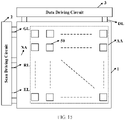
- the display substrate further comprises a non-display region; the non-display region comprises a plurality of voltage control circuits, and each of the plurality of voltage control circuits is coupled to the pixel sub-circuits in at least one row of sub-pixels.
- the display substrate provided by some embodiments of the present disclosure further comprises a plurality of voltage transmission lines in one-to-one correspondence with respective rows of sub-pixels, wherein the pixel sub-circuits in each row of sub-pixels are connected to the voltage control circuit through a voltage transmission line corresponding to the each row of sub-pixels, and the voltage transmission line is configured to transmit the reset voltage and the first power voltage.
- the display substrate comprises a silicon-based base substrate
- the pixel circuit is at least partially formed in the silicon-based base substrate
- the light-emitting element is formed on the pixel circuit
- the light-emitting element comprises one selected from the group consisting of an organic light-emitting diode, a quantum dot light-emitting diode and an inorganic light-emitting diode.
- At least one embodiment of the present disclosure further provides a display apparatus, which comprises: the display substrate according to any one embodiment of the present disclosure.
- At least one embodiment of the present disclosure further provides a driving method corresponding to the pixel circuit according to any one embodiment of the present disclosure, which comprises a reset stage, a data writing stage and a light-emitting stage; in the reset stage, input the reset control signal and the transmission control signal to turn on the voltage control circuit and the voltage transmitting circuit, and apply the reset voltage to the first terminal of the driving circuit through the voltage control circuit and the voltage transmitting circuit, so as to reset the light-emitting element; in the data writing stage, input the scan signal to turn on the data writing circuit, write the data signal into the control terminal of the driving circuit through the date writing circuit, and store, by the data writing circuit, the data signal being written; and in the light-emitting stage, input the light-emitting control signal and the transmission control signal to turn on the voltage control circuit, the voltage transmitting circuit and the driving circuit, and apply the first power voltage to the first terminal of the driving circuit through the voltage control circuit and the voltage transmitting circuit, so that the driving circuit controls the voltage of the second terminal of the driving circuit
- the driving method further comprises a non-light-emitting stage; and in the non-light-emitting stage, stop inputting the transmission control signal to turn off the voltage transmitting circuit, so that the first power voltage is unable to be applied to the first terminal of the driving circuit, to stop the light-emitting element from emitting light.
- the driving method of the pixel circuit further comprises: controlling a display grayscale of the light-emitting element by adjusting a magnitude of the data signal and a time duration of the transmission control signal in the light-emitting stage.
- the controlling the display grayscale of the light-emitting element by adjusting the magnitude of the data signal and the time duration of the transmission control signal in the light-emitting stage comprises: in a case where a target display grayscale of the light-emitting element is less than a preset value, keeping the magnitude of the data signal unchanged, and adjusting the time duration of the transmission control signal at the light-emitting stage to cause the display grayscale of the light-emitting element to conform to the target display grayscale; and in a case where the target display grayscale of the light-emitting element is not less than a preset value, keeping the time duration of the transmission control signal at the light-emitting stage unchanged, and adjusting the magnitude of the data signal to cause the display grayscale of the light-emitting element to conform to the target display grayscale.
- At least one embodiment of the present disclosure further provides a driving method corresponding to the display substrate according to any one embodiment of the present disclosure, which comprises: during a display time period of one frame, causing all rows of sub-pixels to progressively enter a reset stage, a data writing stage and a light-emitting stage; wherein in the reset stage of each row of sub-pixels, input the reset control signal and the transmission control signal to turn on the voltage control circuit and the voltage transmitting circuit, and apply the reset voltage to the first terminal of the driving circuit through the voltage control circuit and the voltage transmitting circuit, so as to reset the light-emitting element; in the data writing stage of each row of sub-pixels, input the scan signal to turn on the data writing circuit, write the data signal into the control terminal of the driving circuit through the date writing circuit, and store, by the data writing circuit, the data signal being written; and in the light-emitting stage of each row of sub-pixels, input the light-emitting control signal and the transmission control signal to turn on the voltage control circuit, the voltage transmit
- the driving method of the display substrate further comprises: during the display time period of one frame, causing all rows of sub-pixels to progressively enter a non-light-emitting stage; wherein in the non-light-emitting stage of each row of sub-pixels, stop inputting the transmission control signal to turn off the voltage transmitting circuit, so that the first power voltage is unable to be applied to the first terminal of the driving circuit, to stop the light-emitting elements of the each row of sub-pixels from emitting light.
- the driving method of the display substrate further comprises: during the display time period of one frame, causing all rows of sub-pixels to simultaneously enter a non-light-emitting stage; wherein in the non-light-emitting stage of all rows of sub-pixels, stop inputting the transmission control signal to turn off the voltage transmitting circuit, so that the first power voltage is unable to be applied to the first terminal of the driving circuit, to stop the light-emitting elements of all rows of sub-pixels from emitting light, simultaneously.
- connection is not intended to define a physical connection or mechanical connection, but may include an electrical connection, directly or indirectly.
- "On,” “under,” “right,” “left” and the like are only used to indicate relative position relationship, and when the position of the object which is described is changed, the relative position relationship may be changed accordingly.
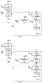
- FIG. 1 is a schematic structural diagram of a silicon-based OLED display device.
- the silicon-based OLED display device includes a silicon-based base substrate 10 and a pixel circuit layer 12 on the silicon-based base substrate.
- the pixel circuit layer 12 can include a plurality of pixel circuits, which are configured to respectively drive a plurality of light-emitting elements (i.e., OLEDs) to be subsequently formed.
- the circuit structure and layout of the pixel circuit can be designed according to actual needs, without being limited in the present disclosure. It should be noted that, for clarity and conciseness, FIG.
- the pixel circuit layer 12 can further include various wirings such as scan signal lines and data signal lines, etc., without being limited in the present disclosure.
- each of the transistors in the pixel circuit layer 12 includes a gate electrode G, a source electrode S, and a drain electrode D.
- these three electrodes are electrically connected to three electrode connection portions, respectively, for example, through via holes filled with tungsten metal (i.e., W-via); furthermore, these three electrodes can be electrically connected to other electrical structures (e.g., transistors, wirings, light-emitting elements, etc.) through the corresponding electrode connection portions, respectively.
- the silicon-based base substrate 10 and the pixel circuit layer 12 can be fabricated in a front-end wafer factory by processing a monocrystalline silicon wafer.
- the silicon-based OLED display device further includes a plurality of light-emitting elements 30 formed on the pixel circuit layer 12.
- each light-emitting element 30 includes a first electrode 22 (for example, as an anode), an organic light-emitting functional layer 24 and a second electrode 26 (for example, as a cathode) that are sequentially stacked.
- the first electrode 22 can be electrically connected to the source electrode S of the transistor T1 in a corresponding pixel circuit through a W-via (and through a connection portion corresponding to the source electrode S); and it can be understood that positions of the source electrode S and the drain electrode D are interchangeable, that is, the first electrode 22 can be electrically connected to the drain electrode D, instead.
- the organic light-emitting functional layer 24 can include an organic light-emitting layer, and can further include one or more selected from the group consisting of an electron injection layer, an electron transport layer, a hole injection layer, and a hole transport layer.
- the second electrode 26 is a transparent electrode; and for example, the second electrode 26 is a common electrode, that is, the plurality of light-emitting elements 30 share a second electrode 26 of an entire surface.
- the light color of the light-emitting element 30 can be white, but is not limited thereto.
- the silicon-based OLED display device further includes a first encapsulation layer 32, a color filter layer 34, a second encapsulation layer 36, and a cover plate 38 that are sequentially disposed on the plurality of light-emitting elements 30.
- the first encapsulation layer 32 and the second encapsulation layer 36 can be polymer or/and ceramic thin film encapsulation layers, but are not limited thereto.
- the color filter layer 34 includes a red filter unit R, a green filter unit G, and a blue filter unit R, but is not limited thereto.
- one filter unit together with a corresponding light-emitting element and a corresponding pixel circuit can be divided into one sub-pixel; and for example, the red filter unit R, the green filter unit G and the blue filter unit R correspond to a red sub-pixel and a green sub-pixel and a blue sub-pixel, respectively.
- the material of the color filter layer 34 can be a material commonly used in the art.
- the cover plate 138 can be a glass cover plate, but is not limited thereto.
- the light-emitting element 30 including the first electrode 22, the organic light-emitting functional layer 24 and the second electrode 26, together with the first encapsulation layer 32, the color filter layer 34, the second encapsulation layer 36 and the cover 38, can all be fabricated in a rear-end panel factory.
- FIG. 1 merely illustratively shows the structure of the display region (also referred to as an active area (AA)) of a silicon-based OLED display device.
- the silicon-based OLED display device can further include a non-display region (a region other than the display region).
- the non-display region can be further divided into a dummy region, a bonding region (BA), and an IC function block, etc.
- the structure of the dummy region is basically the same as that of the display region, which can be used to ensure uniformity of the display region;
- the bonding region includes pads for electrical connection with external circuits and signal transmission;
- the IC function block can be used to set a gate driving circuit (for example, the gate driving circuit is formed by using GOA technique) and circuits with other functions, etc., therein.
- the silicon-based OLED display device has a relatively small pixel size (for example, less than 100 microns), and can be used for micro-display applications.
- the pixel circuit generally includes a plurality of transistors and capacitors. Due to limitations of accuracy in preparation process, the pixel circuit usually occupies a large area in the sub-pixel, which is not conducive to reducing the pixel size or to achieving display of a high resolution (Pixel Per Inch (PPI)).
- the pixel circuit can include a pixel sub-circuit.
- the pixel sub-circuit includes a driving circuit, a voltage transmitting circuit, and a data writing circuit;
- the driving circuit includes a control terminal, a first terminal and a second terminal;
- the voltage transmitting circuit is configured, in response to a transmission control signal, to apply a reset voltage and a first power voltage to the first terminal of the driving circuit, respectively;
- the data writing circuit is configured, in response to a scan signal, to write a data signal into the control terminal of the driving circuit and store the data signal being written;
- the driving circuit is configured to control a voltage of the second terminal of the driving circuit according to the data signal of the control terminal of the driving circuit and the voltage of the first terminal of the driving circuit, and to generate a driving current for driving a light-emitting element to emit light based on the voltage of the second terminal of the driving circuit; and the data writing circuit includes two switching transistors of different types.
- the pixel circuit can further include a voltage control circuit.
- the voltage control circuit is configured to provide the reset voltage to the voltage transmitting circuit in response to a reset control signal, and to provide the first power voltage to the voltage transmitting circuit in response to a light-emitting control signal.
- Some embodiments of the present disclosure further provide, corresponding to the pixel circuit, a driving method, a display substrate, a driving method of the display substrate, and a display apparatus.
- the structure of the pixel sub-circuit is relatively simple, and can be disposed in the sub-pixel in the display region, thereby reducing the area occupied by the pixel circuit in the sub-pixel, which is conducive to achieving display of a high resolution (high PPI); at the same time, the data writing circuit adopts two switching transistors of different types, which can increase a range of the voltage value of the data signal; and in addition, the voltage transmitting circuit provided in the pixel circuit can be used to ensure uniformity of pulse width modulation (PWM) control of the sub-pixel.
- PWM pulse width modulation
- FIG. 2 is a schematic block diagram of a pixel circuit provided by at least one embodiment of the present disclosure. As shown in FIG. 2 , the pixel circuit includes a voltage control circuit 200 and a pixel sub-circuit 100.
- the voltage control circuit 200 is configured to provide a reset voltage Vinit to the pixel sub-circuit 100 (e.g., to provide the reset voltage Vinit to a voltage transmitting circuit 120 in the pixel sub-circuit 100 to be described later) in response to a reset control signal RS, and to provide a first power voltage VDD to the pixel sub-circuit 100 (e.g., to provide the first power voltage VDD to the voltage transmitting circuit 120 in the pixel sub-circuit 100 to be described later) in response to a light-emitting control signal EM.
- the first power voltage VDD can be a driving voltage, such as a high voltage.
- the voltage control circuit 200 includes a first control sub-circuit 210 and a second control sub-circuit 220.
- the first control sub-circuit 210 is configured to provide the reset voltage Vinit to the pixel sub-circuit 100 in response to the reset control signal RS, for example, to provide the reset voltage Vinit to the voltage transmitting circuit 120 in the pixel sub-circuit 100 to be described later.
- the first control sub-circuit 210 in a reset stage, is turned on in response to the reset control signal RS, so as to provide the reset voltage Vinit to the pixel sub-circuit 100, and to reset the light-emitting element L through the pixel sub-circuit 100.
- the second control sub-circuit 220 is configured to provide the first power voltage VDD to the pixel sub-circuit 100 in response to the light-emitting control signal EM, for example, to provide the first power voltage VDD to the voltage transmitting circuit 120 in the pixel sub-circuit 100 to be described later.
- the second control sub-circuit 220 in a light-emitting stage, is turned on in response to the light-emitting control signal EM to provide the first power voltage VDD to the pixel sub-circuit 100, so as to drive the pixel sub-circuit 100 to generate a driving current, and further to drive the light-emitting element L to emit light.
- the light-emitting element L stops emitting light and enters a non-light-emitting stage; and for example, in some examples, after the non-light-emitting stage lasts for a period of time, the light-emitting control signal EM can be input again to, so that the light-emitting element L to return to the light-emitting stage. Therefore, after entering the light-emitting stage, the light-emitting time of the light-emitting element L can be controlled by controlling whether the light-emitting control signal EM is input or not, thereby realizing PWM dimming.
- the pixel sub-circuit 100 includes a driving circuit 110, a voltage transmitting circuit 120 and a data writing circuit 130.
- the driving circuit 110 includes a control terminal 111, a first terminal 112 and a second terminal 113, and is configured to control a voltage of the second terminal 113 according to a voltage of the control terminal 111 (e.g., a voltage of a data signal) and a voltage of the first terminal 112 (e.g., the first power voltage), and to generate a driving current for driving the light-emitting element L to emit light based on the voltage of the second terminal 113.
- a voltage of the control terminal 111 e.g., a voltage of a data signal
- the first terminal 112 e.g., the first power voltage
- the driving circuit 110 can control a voltage Vs of the second terminal 113 according to the voltage of the control terminal 111 (e.g., the voltage of the data signal) and the voltage of the first terminal 112 (e.g., the first power voltage VDD), and generate a driving current based on the voltage Vs, so as to provide the driving current to the light-emitting element L to drive the light-emitting element L to emit light, and to provide a corresponding driving current according to a grayscale desired to be displayed to drive the light-emitting element L to emit light.
- the voltage of the control terminal 111 e.g., the voltage of the data signal
- the voltage of the first terminal 112 e.g., the first power voltage VDD
- the grayscale displayed by the light-emitting element L is not only related to a magnitude of the driving current, but also related to a time duration in which the driving current is applied to the light-emitting element L (i.e., the light-emitting time of the light-emitting element L).
- the voltage transmitting circuit 120 is configured, in response to a transmission control signal VT, to apply the reset voltage Vinit and the first power voltage VDD to the first terminal 112 of the driving circuit 110, respectively.
- the voltage transmitting circuit 120 in the reset stage, is turned on in response to the transmission control signal VT, so as to apply the reset voltage Vinit provided by the first control sub-circuit 210 to the first terminal 112 of the driving circuit 110; because the driving circuit 110 remains in an on state under the control of the data signal of a previous frame, the reset voltage Vinit can be transmitted to the light-emitting element L through the driving circuit 110, so as to reset the light-emitting element L.
- the voltage transmitting circuit 120 is turned on in response to the transmission control signal VT, so as to apply the first power voltage VDD provided by the second control sub-circuit 220 to the first terminal 112 of the driving circuit 110; because the driving circuit 110 remains in an on state under the control of the data signal in a current frame, the driving circuit 110 can generate a driving current under the drive of the first power voltage VDD, so as to drive the light-emitting element L to emit light.
- the voltage transmitting circuit 120 can be controlled to be turned on or off by controlling whether the transmission control signal VT is input or not, so as to control the light-emitting time of the light-emitting element L, and further to realize PWM dimming.
- specific details can be referred to the related description of controlling the light-emitting time of the light-emitting element L by controlling whether the light-emitting control signal EM is input or not, and will not be repeated here.
- the light-emitting time of the light-emitting element L can be controlled by controlling whether or not to input the light-emitting control signal EM and/or the transmission control signal VT, which is not limited in the embodiment of the present disclosure.
- the data writing circuit 130 is configured, in response to a scan signal SN, to write a data signal DATA into the control terminal 111 of the driving circuit 110 and store the data signal DATA being written.
- the data writing circuit 130 further includes a storage capacitor, which can receive and store the data signal DATA being written.
- the data writing circuit 130 in a data writing stage, is turned on in response to the scan signal SN, so as to write the data signal DATA into the control terminal 111 of the driving circuit 110; and meanwhile, the storage capacitor can store the data signal DATA being written, and then the data signal DATA being stored can be used to control the driving circuit 110 in the light-emitting stage, so that the driving circuit 110 generates a driving current to drive the light-emitting element L to emit light based on the data signal DATA.
- the data writing circuit includes two switching transistors of different types, and for example, the two switching transistors are turned on in response to the scan signal SN. For example, specifically, one of the two switching transistors is turned on in response to the scan signal SN, and the other of the two switching transistors is turned on in response to an inverted signal SN' of the scan signal SN.
- a first electrode (e.g., an anode) of the light-emitting element L is coupled to the second terminal 113 of the driving circuit 110, and a second electrode (e.g., a cathode) is coupled to a second power terminal to receive a second power voltage VSS.
- the second power voltage VSS can be a low voltage; and for example, the second power voltage VSS can be a zero voltage or a ground voltage.
- FIG. 3 is a schematic block diagram of another pixel circuit provided by at least one embodiment of the present disclosure. As shown in FIG. 3 , on the basis of the pixel circuit shown in FIG. 2 , the pixel circuit shown in FIG. 3 further includes a current transmitting circuit 140. It should be noted that other circuit structures (such as the voltage control circuit 200, the driving circuit 110, the voltage transmitting circuit 120, the data writing circuit 130, etc.) in the pixel circuit shown in FIG. 3 are basically the same as those of the pixel circuit shown in FIG. 2 , and details will not be repeated here.
- other circuit structures such as the voltage control circuit 200, the driving circuit 110, the voltage transmitting circuit 120, the data writing circuit 130, etc.
- the first electrode (e.g., the anode) of the light-emitting element L is coupled to the second terminal 113 of the driving circuit 110 through the current transmitting circuit 140, and the second electrode (e.g., the cathode) is coupled to the second power terminal to receive the second power voltage VSS.
- the current transmitting circuit 140 is configured to transmit the driving current generated by the driving circuit 110 to the light-emitting element L.
- a control terminal of the current transmitting circuit 140 is connected to a second voltage terminal to receive a second voltage V2, and the current transmitting circuit 140 is substantially kept in an on state under the control of the second voltage V2; thus, in the reset stage, the current transmitting circuit 140 allows the reset voltage Vinit to be transmitted to the light-emitting element L, and in the light-emitting stage, the current transmitting circuit 140 allows the driving current generated by the driving circuit 110 to be transmitted to the light-emitting element L.
- the current transmitting circuit 140 can function as a current clamp.
- the current transmitting circuit 140 has a relatively high on degree under the control of the second voltage V2 and the voltage of the second terminal of the driving circuit 110, so that the light-emitting element L can have a relatively high light-emitting brightness;
- the current transmitting circuit 140 has a relatively low on degree under the control of the second voltage V2 and the voltage of the second terminal of the driving circuit 110, so that the light-emitting element L can have a relatively low light-emitting brightness;
- the current transmitting circuit 140 has an extremely low on degree (e.g., close to an off state) under the control of the second voltage V2 and the voltage of the second terminal of the driving circuit 110, so that the light-emitting element L basically does not emit light.
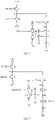
- FIG. 4 is a schematic circuit diagram of a specific implementation example of the pixel circuit shown in FIG. 2 .
- the pixel sub-circuit 100 includes a driving transistor M0, a first switching transistor M1, a second switching transistor M2, a third switching transistor M3, a fourth switching transistor M, a fifth switching transistor M5, and a storage capacitor Cst.
- FIG. 4 also shows the light-emitting element L.
- the light-emitting element L can include one selected from the group consisting of an organic light-emitting diode, a quantum dot light-emitting diode, and an inorganic light-emitting diode.
- the light-emitting element L can adopt a micron-level light-emitting element, such as a Micro-LED, a Mini-LED, etc., and the embodiments of the present disclosure include but are not limited thereto. It should be noted that the types of the switching transistors in FIG. 4 are all illustrative, and should not be considered as limitations to the embodiments of the present disclosure.
- the first control sub-circuit 210 in the voltage control circuit 200 can be implemented as the first switching transistor M1.
- a gate electrode of the first switching transistor M1 is connected to a reset control signal terminal to receive the reset control signal RS, a first electrode of the first switching transistor M1 is connected to a reset voltage terminal to receive the reset voltage Vinit, and a second electrode of the first switching transistor M1 is connected to a first node N1.
- the first switching transistor M1 can be an N-type transistor, and the embodiments of the present disclosure include but are not limited thereto.
- the reset voltage Vinit can be a zero voltage or a ground voltage, or can be any other fixed voltage, such as a low voltage, etc., without being limited in the embodiments of the present disclosure.
- the reset control signal RS is at a high level
- the N-type first switching transistor M1 is turned on; and in the case where the reset control signal RS is at a low level, the N-type first switching transistor M1 is turned off.
- the second control sub-circuit 220 in the voltage control circuit 200 can be implemented as the second switching transistor M2.
- a gate electrode of the second switching transistor M2 is connected to the light-emitting control signal terminal to receive the light-emitting control signal EM
- a first electrode of the second switching transistor M2 is connected to the first power terminal to receive the first power voltage VDD
- a second electrode of the second switching transistor M2 is connected to the first node N1.
- the second switching transistor M2 can be a P-type transistor, and the embodiments of the present disclosure include but are not limited thereto.
- the first power voltage VDD can be a driving voltage, such as a high voltage.
- the P-type second switching transistor M2 is turned on; and in the case where the light-emitting control signal EM is at a high level, the P-type second switching transistor M2 is turned off.
- the voltage transmitting circuit 120 in the pixel sub-circuit 100 can be implemented as the third switching transistor M3.
- a gate electrode of the third switching transistor M3 is connected to a transmission control signal terminal to receive the transmission control signal VT, a first electrode of the third switching transistor M3 is connected to the first node N1, and a second electrode of the third switching transistor M3 is connected to a second node N2.
- the third switching transistor M3 can be an N-type transistor, and the embodiments of the present disclosure include but are not limited thereto.
- the N-type third switching transistor M3 is turned on; and in the case where the transmission control signal VT is at a low level, the N-type third switching transistor M3 is turned off.
- the driving circuit 110 in the pixel sub-circuit 100 can be implemented as the driving transistor M0.
- a gate electrode of the driving transistor M0 serves as the control terminal 111 of the driving circuit 110 and is connected to a fourth node N4, a first electrode of the driving transistor M0 serves as the first terminal 112 of the driving circuit 110 and is connected to the second node N2, and a second electrode of the driving transistor M0 serves as the second terminal 113 of the driving circuit 110 and is connected to a third node N3.
- the driving transistor M0 can be an N-type transistor, and the embodiments of the present disclosure include but are not limited thereto.
- the data writing circuit 130 in the pixel sub-circuit 100 can be implemented as the fourth switching transistor M4 and the storage capacitor Cst.
- a gate electrode of the fourth switching transistor M4 is connected to a scan signal terminal to receive the scan signal SN
- a first electrode of the fourth switching transistor M4 is connected to a data signal terminal to receive the data signal DATA
- a second electrode of the fourth switching transistor M4 is connected to the first fourth node N4
- a first terminal of the storage capacitor Cst is connected to the fourth node N4 (i.e., coupled to the gate electrode of the driving transistor M0)
- a second terminal of the storage capacitor Cst is connected to a first voltage terminal to receive a first voltage V1.
- the first voltage V1 can be a fixed voltage, such as a zero voltage or a ground voltage.
- the storage capacitor Cst can store the data signal DATA written into the fourth node N4 (i.e., the gate electrode of the driving transistor M0).
- the fourth switching transistor M4 can be an N-type transistor, and the embodiments of the present disclosure include but are not limited thereto. For example, in the case where the scan signal SN is at a high level, the N-type fourth switching transistor M4 is turned on; and in the case where the scan signal SN is at a low level, the N-type fourth switching transistor M4 is turned off.
- the data writing circuit 130 in the pixel sub-circuit 100 can further include a fifth switching transistor M5, that is, the data writing circuit 130 can be implemented as the fourth switching transistor M4, the fifth switching transistor M5 and the storage capacitor Cst.
- a gate electrode of the fifth switching transistor M5 is configured to receive an inverted signal SN' of the scan signal SN, a first electrode of the fifth switching transistor M5 is connected to the data signal terminal to receive the data signal DATA, and a second electrode of the fifth switching transistor M5 is connected to the fourth node N4.
- the fifth switching transistor M5 and the fourth switching transistor M4 are of different types; for example, as shown in FIG.
- the fifth switching transistor M4 is a P-type transistor.
- the fifth switching transistor M5 and the fourth switching transistor M4 can be turned on at the same time and can be turned off at the same time.
- the fifth switching transistor M5 and the fourth switching transistor M4 can be transistor devices with symmetrical structures; and for example, the fifth switching transistor M5 and the fourth switching transistor M4 can form a transmission gate (also referred to as an analog switch).
- the inverted signal SN' of the scan signal SN can be obtained by inputting the scan signal SN to an inverter circuit, and the embodiments of the present disclosure include but are not limited thereto.
- the scan signal SN can be input to an input terminal of the inverter circuit, so that the inverted signal SN' is output by an output terminal of the inverter circuit.
- the inverter circuit can be provided in each sub-pixel in the display region AA, or can be provided in the non-display region NA and be set to transmit the inverted signal SN' of the scan signal SN to each row of sub-pixels through wiring.
- the inverter circuit can be implemented in a common way, which will not be repeated here.
- the data writing circuit 130 includes only the fourth switching transistor M4
- the influence of a threshold voltage and an internal resistance of the fourth switching transistor M4 is necessary to be considered in general, so that the data signal DATA has a relatively small range of voltage value.
- the case in which the data writing circuit 130 includes only the fifth switching transistor M5 is similar to the case in which the data writing circuit 130 includes only the fourth switching transistor M4, and details will not be repeated here.
- the influence of threshold voltages and internal resistances of the two switching transistors is small, so that the range of voltage value of the data signal DATA can be enlarged.
- the operation principle of the fifth switching transistor M5 and the fourth switching transistor M4 i.e., the principle of enabling the data signal DATA to have a larger range of voltage value
- the operation principle of a common CMOS transmission gate which is used in an analog circuit can be referred to the operation principle of a common CMOS transmission gate which is used in an analog circuit, and details will not be repeated here.
- a first electrode (e.g., an anode) of the light-emitting element L is coupled to the second electrode of the driving transistor M0, and a second electrode (e.g., a cathode) of the light-emitting element L is coupled to the second power terminal to receive the second power voltage VSS.
- the second power voltage VSS can be a low voltage, and for example, the second power voltage VSS can be a zero voltage or a ground voltage.
- FIG. 5 is a schematic circuit diagram of a specific implementation example of the pixel circuit shown in FIG. 3 .
- the pixel circuit shown in FIG. 5 further includes a sixth switching transistor M6.
- other circuit structures such as the driving transistor M0, the first to fifth switching transistors M1-M5, the storage capacitor Cst, etc.
- the current transmitting circuit 140 in the pixel sub-circuit 100 can be implemented as the sixth switching transistor M6.
- a gate electrode of the sixth switching transistor M6 is connected to the second voltage terminal to receive a second voltage V2
- a first electrode of the sixth switching transistor M6 is connected to the third node N3
- a second electrode of the sixth switching transistor M6 is coupled to the first electrode (e.g., the anode) of the light-emitting element L
- the second electrode (e.g., cathode) of the light-emitting element L is connected to the second power terminal to receive the second power voltage VSS.
- the first electrode e.g., the anode
- the second electrode e.g., cathode
- the sixth switching transistor M6 can be a P-type transistor, and the embodiments of the present disclosure include but are not limited thereto.
- the second voltage V2 can be a zero voltage or a ground voltage, or can be any other fixed voltage, such as a low voltage.
- the sixth switching transistor M6 is substantially kept in an on state under the control of the second voltage V2.
- the storage capacitor Cst can be a capacitance device manufactured by a process.
- the capacitor device is implemented by manufacturing specific capacitor electrodes, and respective electrodes of the capacitor can be implemented by a metal layer, a semiconductor layer (e.g., doped poly-silicon) etc.
- the capacitor can also be a parasitic capacitance between various devices, which can be realized by a transistor itself and other devices and wirings.
- a connection mode of the capacitor is not limited to the mode described above, or can be any other suitable connection mode as long as the voltage of the corresponding node can be stored.
- the first node N1, the second node N2, the third node N3, and the fourth node N4 do not represent components that must actually exist, but represent junction points of related electrical connections in the circuit diagram.
- all the transistors used in the embodiments of the present disclosure can be thin film transistors, field effect transistors, or other switching devices with the same characteristics, without being limited in the embodiments of the present disclosure.
- the source electrode and the drain electrode of the transistor used here can be symmetrical in structure, so the source electrode and the drain electrode can be structurally indistinguishable.
- one of the electrodes is a first electrode and the other electrode is a second electrode.
- the first electrode can be a source electrode and the second electrode can be a drain electrode; and taking an N-type transistor as an example, the first electrode can be a drain electrode and the second electrode can be a source electrode.
- the embodiments of the present disclosure do not limit the type of each transistor. In a specific implementation, it is only necessary to connect the electrodes of a selected type of transistor with reference to the electrodes of the corresponding transistor in the embodiments of the present disclosure, and to cause the corresponding voltage terminal to provide the corresponding high voltage or low voltage.
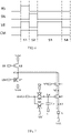
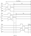
- FIG. 6 is a signal timing chart of a driving method of a pixel circuit provided by at least one embodiment of the present disclosure.
- the driving method of the pixel circuit provided by the embodiment of the present disclosure will be described below with reference to the signal timing chart shown in FIG. 6 .
- level of potential in the signal timing chart shown in FIG. 6 is merely illustrative, and does not represent a true potential value or a relative proportion.
- a low-level signal corresponds to a turn-on signal of the P-type transistor, while a high-level signal corresponds to a turn-off signal of the P-type transistor.
- the driving method provided in the present embodiment can include four stages, namely a reset stage S1, a data writing stage S2, a light-emitting stage S3, and a non-light-emitting stage S4.
- FIG. 6 shows timing waveforms of the control signals (the reset control signal RS, the scan signal SN, the transmission control signal VT and the light-emitting control signal EM) in each stage.
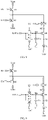
- FIGS. 7-10 are schematic circuit diagrams of the circuit shown in FIG. 4 corresponding to the four stages in FIG. 6 .
- FIG. 7 is a schematic circuit diagram when the pixel circuit shown in FIG. 4 is in the reset stage S1
- FIG. 8 is a schematic circuit diagram when the pixel circuit shown in FIG. 4 is in the data writing stage S2
- FIG. 9 is a schematic circuit diagram when the pixel circuit shown in FIG. 4 is in the light-emitting stage S3
- FIG. 10 is a schematic circuit diagram when the pixel circuit shown in FIG. 4 is in the non-light-emitting stage S4.
- FIGS. 7-10 indicates that the transistor itself is in an off state in the corresponding stage, and a dashed line with an arrow in FIGS. 7-10 indicates a current path of the pixel circuit in the corresponding stage (the direction of the arrow does not indicate a current direction).
- the reset control signal RS and the transmission control signal VT are input, the voltage control circuit 200 and the voltage transmitting circuit 120 are turned on, and the reset voltage Vinit is applied to the first terminal 112 of the driving circuit 110 through the voltage control circuit 200 and the voltage transmitting circuit 120, so as to reset the light-emitting element L.
- the voltage control circuit 200 is turned on by turning on the first control sub-circuit 210, and the reset voltage Vinit is applied to the first terminal 112 of the driving circuit 110 through the first control sub-circuit 210 and the voltage transmitting circuit 120.
- the N-type first switching transistor M1 is turned on by the high level of the reset control signal RS, and the N-type third switching transistor M3 is turned on by the high level of the transmission control signal VT; meanwhile, the P-type second switching transistor M2 is turned off by the high level of the light-emitting control signal EM, the N-type fourth switching transistor M4 is turned off by the low level of the scan signal SN, and correspondingly, the P-type fifth switching transistor M5 is turned off by the high level of the inverted signal SN' of the scan signal SN; in addition, the driving transistor M0 is turned on by the voltage of the fourth node N4 (that is, the data signal DATA stored by the storage capacitor Cst during the display process of a previous frame of picture).
- a reset path (as indicated by the dashed line with an arrow in FIG. 7 ) can be formed. Because the reset voltage Vinit is a low voltage (for example, a ground voltage or a zero voltage), the light-emitting element L can be reset through the reset path.
- the scan signal SN is input, the data writing circuit 130 is turned on, the data signal DATA is written into the control terminal 111 of the driving circuit 110 through the data writing circuit 130, and the data writing circuit 130 stores the data signal DATA being written.
- the N-type fourth switching transistor M4 is turned on by the high level of the scan signal SN, and correspondingly, the P-type fifth switching transistor M5 is turned on by the low level of the inverted signal SN' of the scan signal SN; meanwhile, the N-type first switching transistor M1 is turned off by the low level of the reset control signal RS, the P-type second switching transistor M2 is turned off by the high level of the light-emitting control signal EM, and the N-type third switching transistor M3 is turned off by the low level of the transmission control signal VT.
- a data writing path (as indicated by a dashed line with an arrow in FIG. 8 ) can be formed.
- the data signal DATA charges the first terminal (i.e., the fourth node N4, namely, the gate electrode of the driving transistor M0) of the storage capacitor Cst through the data writing path, so that the potential at the first terminal of the storage capacitor Cst becomes DATA, and the driving transistor M0 remains in an ON state under the control of the data signal DATA.
- the potential at the first terminal of the storage capacitor Cst (i.e., the fourth node N4, that is, the gate electrode of the driving transistor M0) is DATA, that is, the voltage information of the data signal DATA is stored in the storage capacitor Cst, so as to be used to control the driving transistor M0 to generate a driving current in the subsequent light-emitting stage.
- the light-emitting control signal EM and the transmission control signal VT are input, the voltage control circuit 200, the voltage transmitting circuit 120, and the driving circuit 110 are turned on, and the first power voltage VDD is applied to the first terminal 112 of the driving circuit 110 through the voltage control circuit 200 and the voltage transmitting circuit 120, so that the driving circuit 110 controls the voltage Vs of the second terminal 113 of the driving circuit 110 according to the data signal DATA of the control terminal 111 of the driving circuit 110 and the first power voltage VDD of the first terminal 112 of the driving circuit 110, and generates a driving current to drive the light-emitting element L to emit light based on the voltage Vs of the second terminal 113 of the driving circuit 110.
- the voltage control circuit 200 is turned on by turning on the second control sub-circuit 220, and the first power voltage VDD is applied to the first terminal 112 of the driving circuit 110 through the second control sub-circuit 220 and the voltage transmitting circuit 120.
- the P-type second switching transistor M2 is turned on by the low level of the light-emitting control signal EM, and the N-type third switching transistor M3 is turned on by the high level of the transmission control signal VT; meanwhile, the N-type first switching transistor M1 is turned off by the low level of the reset control signal RS, the N-type fourth switching transistor M4 is turned off by the low level of the scan signal SN, and correspondingly, the P-type fifth switching transistor M5 is turned off by the high level of the inverted signal SN' of the scan signal SN; in addition, the driving transistor M0 is turned on by the voltage of the fourth node N4 (i.e., the data signal DATA stored in the storage capacitor Cst in the data writing stage S2).
- a light-emitting path (as shown by a dashed line with an arrow in FIG. 9 ) can be formed.
- the first electrode (the anode) of the light-emitting element L is accessed to the first power voltage VDD (high voltage) through the light-emitting path, and the second electrode (the cathode) of the light-emitting element L is accessed to the second power voltage VSS (low voltage), so that the light-emitting element L can emit light under the action of the driving current flowing through the driving transistor M0.
- the driving transistor M0 operates in a sub-threshold region; and it should be noted that in the embodiment of the present disclosure, when the driving transistor M0 operates in the threshold region, the driving transistor M0 is considered to be turned on.
- I L represents a driving current
- Vth represents a threshold voltage of the driving transistor M0
- Vgs represents a voltage difference between the gate electrode and the second electrode (e.g., source electrode) of the driving transistor M0
- Vs represents a voltage of the second electrode of the driving transistor M0
- q is an electron charge (a constant value)
- n is a channel doping concentration of the driving transistor M0
- k is a constant value
- T is an operating temperature of the driving transistor M0.
- the voltage Vs of the second electrode of the driving transistor M0 can be changed by adjusting the voltage of the gate electrode of the driving transistor M0 (i.e., the voltage of the data signal DATA), thereby changing the voltage difference between the two electrodes of the light-emitting element L, and further adjusting the light-emitting brightness of the light-emitting element L.
- the grayscale of light emission of the pixel circuit is not only related to the magnitude of the driving current, but also related to a time duration in which the driving current is applied to the light-emitting element (i.e., the light-emitting time of the light-emitting element).
- the relationship between the grayscale of light emission of the pixel circuit and the magnitude of the driving current and the length of the light-emitting time can be determined via theoretical calculations, simulations, experimental measurements, etc.
- a desired grayscale can be displayed by simultaneously controlling the magnitude of the driving current and the length of the light-emitting time.
- the above driving method can insert a non-light-emitting stage S4 after the light-emitting stage S3 to control the length of the light-emitting time of the light-emitting element.
- the input of the transmission control signal VT is stopped, and the voltage transmitting circuit 120 is turned off, so that the first power voltage VDD cannot be applied to the first terminal 112 of the driving circuit 110, so as to cause the light-emitting element L to stop emitting light.
- the input of the transmission control signal VT can be stopped (other control signals remain in the states in the light-emitting stage S3); for example, the transmission control signal VT is changed from the high level to the low level, to cause the third switching transistor M3 to be turned off, so that the first power voltage VDD cannot be applied to the first terminal of the driving transistor M0, the light-emitting path in FIG. 9 is disconnected, the driving transistor M0 cannot generate a driving current, and the light-emitting element L stops emitting light, that is, enters the non-light-emitting stage S4.
- the transmission control signal VT can be input again so that the light-emitting element L returns to the light-emitting stage S3, that is, the light-emitting stage S3 and the non-light-emitting stage S4 can be alternated.
- PWM dimming can be achieved.
- the switching between the light-emitting stage S3 and the non-light-emitting stage S4 can also be realized by using other methods, and is not limited to the above-mentioned method.
- the switching between the light-emitting stage S3 and the non-light-emitting stage S4 can be realized by controlling whether or not to input the light-emitting control signal EM.
- the switching between the light-emitting stage S3 and the non-light-emitting stage S4 can also be realized by simultaneously controlling whether or not to input the light-emitting control signal EM and the transmission control signal VT.
- the current transmitting circuit 140 is substantially kept in an on state under the control of the second voltage V2, the pixel circuit shown in FIG. 3 (for example, specifically implemented as the circuit structure shown in FIG. 5 ) can also be driven based on the timing chart of the various control signals shown in FIG. 6 . Specific details can be referred to the related description of the foregoing driving method, and will not be repeated here.
- the signal timing chart shown in FIG. 6 is illustrative.
- the signal timing thereof during operation can be determined according to actual needs, which is not limited in the embodiment of the present disclosure.
- FIG. 11 is a schematic diagram of a principle of controlling a display grayscale in a driving method of a pixel circuit provided by at least one embodiment of the present disclosure.
- each sub-pixel can display a desired grayscale by simultaneously controlling the magnitude of the driving current and the length of the light-emitting time (i.e., the duration of the foregoing light-emitting stage described above).
- the magnitude of the driving current can be controlled correspondingly by adjusting the magnitude of the data signal DATA, and for example, this process can be referred to the foregoing formula of the driving current.
- the length of the light-emitting time of the light-emitting element can be controlled by controlling the time duration of the light-emitting stage, and for example, the switching between the light-emitting stage and the non-light-emitting stage can be realized by controlling whether or not to input the light-emitting control signal EM and/or the transmission control signal VT, so as to control the length of the light-emitting time.
- the driving method provided by the embodiment of the present disclosure can further include: controlling the display grayscale of the light-emitting element by adjusting the magnitude of the data signal DATA and the time duration of the transmission control signal VT in the light-emitting stage.
- controlling the display grayscale of the light-emitting element by adjusting the magnitude of the data signal DATA and the time duration of the transmission control signal VT in the light-emitting stage.
- the magnitude of the data signal DATA is kept unchanged (correspondingly, the light-emitting brightness of the light-emitting element remains unchanged), and the time duration of the transmission control signal VT in the light-emitting stage (i.e., the light-emitting time of the light-emitting element) is adjusted to cause the display grayscale of the light-emitting element to conform to the target display grayscale; and in the case where the target display grayscale of the light-emitting element is not less than the preset value (that is, the target display grayscale is between G0 ⁇ Gmax, Gmax is the highest grayscale), the time duration of the transmission control signal VT at the light-emitting stage is kept unchanged, and the magnitude of the data signal DATA is adjusted to cause the display grayscale of the light-emitting element to conform
- the preset value GO can be determined according to actual needs, without being limited in the embodiment of the present disclosure. It should also be noted that the corresponding relationship between the data signal and the display grayscale (as shown by a solid lines and solid dots in the figure) and the corresponding relationship between the time duration of the light-emitting stage and the display grayscale (as shown by a dashed line and hollow circles in the figure) as shown in FIG. 14 are both illustrative, and both of them can be determined according to actual needs, without being limited in the embodiment of the present disclosure.
- FIG. 12 is a schematic structural diagram of a display substrate provided by at least one embodiment of the present disclosure.
- the display substrate includes the pixel circuit provided by any one of the above embodiments of the present disclosure.
- the display substrate can be a silicon-based base substrate, and the embodiments of the present disclosure include but are not limited thereto.
- a cross-sectional view of the structure of the display substrate can be referred to that of the structure of the silicon-based OLED display device shown in FIG. 1 .
- the pixel circuit (referring to the transistor shown in FIG. 1 ) can be at least partially formed in the silicon-based base substrate, and the light-emitting element can be formed on the pixel circuit.
- the related description of the silicon-based OLED display device shown in FIG. 1 which will not be repeated here.
- the display substrate includes a display region AA and a non-display region NA.
- the non-display region NA is a region other than the display region AA on the display substrate.
- the non-display region NA surrounds the display region AA
- the display region AA of the display substrate includes a plurality of sub-pixels 50 arranged in an array.
- the plurality of sub-pixels 50 can include multiple kinds of color sub-pixels, such as red sub-pixels, green sub-pixels, blue sub-pixels, etc.
- the embodiments of the present disclosure include but are not limited thereto.
- the arrangement manner of the multiple kinds of color sub-pixels can be determined according to actual needs, without being limited in the embodiments of the present disclosure.
- each sub-pixel 50 includes a light-emitting element L and a pixel sub-circuit 100 coupled to the light-emitting element L, and the pixel sub-circuit 100 can be configured to drive the light-emitting element L to emit light. That is, the pixel sub-circuit 100 in the above-mentioned pixel circuit can be disposed in the display region AA of the display substrate.
- the light-emitting element L can include an organic light-emitting diode (OLED), and the embodiments of the present disclosure include but are not limited thereto; and for example, the light-emitting element L can also include a quantum dot light-emitting diode (QLED) or an inorganic light-emitting diode, etc.
- the light-emitting element L can adopt a micron-level light-emitting element, such as a Micro-LED, a Mini-LED, etc.
- the embodiments of the present disclosure include but are not limited thereto.
- the non-display region NA includes a plurality of voltage control circuits 200, and each voltage control circuit 200 is coupled to the pixel sub-circuits 100 in at least one row of sub-pixels 50. That is, the voltage control circuit in the above pixel circuit can be disposed in the non-display region NA of the display substrate.
- the light-emitting time of the light-emitting elements L of at least one row (e.g., one or a plurality of rows) of sub-pixels coupled to one voltage control circuit 200 can be controlled by controlling whether or not to input the light-emitting control signal EM.
- the display substrate further includes a plurality of voltage transmission lines VL in one-to-one correspondence with respective rows of sub-pixels 50.
- the pixel sub-circuits 100 in each row of sub-pixels 50 are connected to the voltage control circuit 200 through a voltage transmission line VL corresponding to the each row of sub-pixels, and the voltage transmission line VL is configured to transmit the reset voltage Vinit and the first power voltage VDD provided by the voltage control circuit 200 to the pixel sub-circuit 100.
- wirings such as a first power line for transmitting the first power voltage VDD, a reset control signal line for transmitting the reset control signal RS, and a light-emitting control signal line for transmitting the light-emitting control signal EM, can also be disposed in the non-display region NA accordingly.
- a layout of wirings in the display region AA of the display substrate can be simplified, so that more sub-pixels 50 (that is, the pixel sub-circuits 100 and the light-emitting elements L, etc.) can be disposed in the display region AA, which is conducive to achieving display of a high resolution (high PPI).
- the voltage transmitting circuits 120 in the pixel sub-circuits 100 of each row of sub-pixels 50 can be connected to a same transmission control signal line, and the same transmission control signal line provides the transmission control signal VT; thus, after entering the light-emitting stage, the light-emitting time of the light-emitting elements L of each row of sub-pixels can be controlled by controlling whether or not to input the transmission control signal VT.
- the voltage transmitting circuit 120 is located at an inner side of the sub-pixel 50 while the second control sub-circuit 220 is located at an outer side of the sub-pixel 50 (located in the non-display region NA), compared with a PWM control based on the second control sub-circuit 220 (i.e., to control whether or not to input the light-emitting control signal EM), a PWM control based on the voltage transmitting circuit 120 (i.e., to control whether or not to input the transmission control signal VT) can reduce the influence of the wiring load (e.g., parasitic capacitance and parasitic resistance, etc.), thereby better ensuring uniformity of the PWM control of the sub-pixels.
- the wiring load e.g., parasitic capacitance and parasitic resistance, etc.
- FIG. 12 merely illustratively shows a case in which each voltage control circuit 200 is coupled to the pixel sub-circuits 100 in a row of sub-pixels 50.
- the embodiments of the present disclosure include but are not limited thereto.
- each voltage control circuit 200 can also be coupled to the pixel sub-circuits 100 in a plurality of rows (e.g., two rows, three rows, four rows, etc., and for example, the plurality of rows includes adjacent rows) of sub-pixels 50.
- the display substrate provided by the embodiments of the present disclosure is provided with a voltage control circuit 200 in the non-display region NA, which can simplify the structure of the pixel sub-circuit 100 in each sub-pixel 50 and reduce an occupied area of the pixel sub-circuit 100 in each sub-pixel 50. Therefore, more sub-pixels 50 (that is, the pixel sub-circuits 100 and the light-emitting elements L, etc.) can be disposed in the display region AA, which is beneficial to achieving display of a high resolution (high PPI).
- FIG. 13 is a signal timing chart of a driving method of a display substrate provided by at least one embodiment of the present disclosure.
- the signal timing chart shown in FIG. 6 can be used to drive a row of sub-pixels in the display substrate provided by the embodiments of the present disclosure, while the signal timing chart shown in FIG. 13 can be used to drive the display substrate (i.e., to drive all rows of sub-pixels in the display substrate).
- the signal timing sequences corresponding to each row of sub-pixels are basically the same as the signal timing sequences shown in FIG. 6 , that is, the operation principle of each row of sub-pixels can be referred to the related description of the foregoing driving method, which will not be repeated here.
- the driving method of the display substrate includes: during a display time period of one frame, causing all rows of sub-pixels to progressively enter a reset stage, a data writing stage, and a light-emitting stage.
- the signal timing sequences corresponding to the reset stage, the data writing stage and the light-emitting stage of each row of sub-pixels can be referred to the signal timing sequences corresponding to the reset stage, the data writing stage and the light-emitting stage shown in FIG. 6 .
- the reset control signal RS and the transmission control signal VT are input, the voltage control circuit 200 and the voltage transmitting circuit 120 are turned on, and the reset voltage Vinit is applied to the first terminal 112 of the driving circuit 110 through the voltage control circuit 200 and the voltage transmitting circuit 120, so as to reset the light-emitting elements L of the each row of sub-pixels.
- the voltage control circuit 200 is turned on by turning on the first control sub-circuit 210, and the reset voltage Vinit is applied to the first terminal 112 of the driving circuit 110 through the first control sub-circuit 210 and the voltage transmitting circuit 120.
- specific details can be referred to the related description of the reset stage S1 in the driving method of the pixel circuit mentioned above, and will not be repeated here.
- the scan signal SN is input, the data writing circuit 130 is turned on, and the data signal DATA is written into the control terminal 111 of the driving circuit 110 through the data writing circuit 130, and the data writing circuit 130 stores the data signal DATA being written.
- specific details can be referred to the related description to the related description of the data writing stage S2 in the driving method of the pixel circuit mentioned above, and will not be repeated here.
- the light-emitting control signal EM and the transmission control signal VT are input, the voltage control circuit 200, the voltage transmitting circuit 120 and the driving circuit 110 are turned on, and the first power voltage VDD is applied to the first terminal 112 of the driving circuit 110 through the voltage control circuit 200 and the voltage transmitting circuit 120, so that the driving circuit 110 controls the voltage Vs of the second terminal 113 of the driving circuit 110 according to the data signal DATA of the control terminal 111 of the driving circuit 110 and the first power voltage VDD of the first terminal 112 of the driving circuit 110, and generates a driving current for driving the light-emitting elements L of the each row of sub-pixels to emit light based on the voltage Vs of the second terminal 113 of the driving circuit 110.
- the voltage control circuit 200 is turned on by turning on the second control sub-circuit 220, and the first power voltage VDD is applied to the first terminal 112 of the driving circuit 110 through the second control sub-circuit 220 and the voltage transmitting circuit 120.
- specific details can be referred to the related description to the related description of the light-emitting stage S3 in the driving method of the pixel circuit mentioned above, and will not be repeated here.
- the driving method of the display substrate can further include: during the display time period of one frame, causing all rows of sub-pixels to progressively enter a non-light-emitting stage.
- the light-emitting elements of all row of sub-pixels can enter the non-light-emitting stage S4 from the light-emitting stage progressively by stopping the input of the transmission control signal VT.
- the embodiments of the present disclosure include but are not limited to such a method of realizing the switching between the light-emitting stage and the non-light-emitting stage, and for example, other methods can be referred to the related descriptions in the driving method of the pixel circuit mentioned above.
- the input of the transmission control signal VT is stopped, the voltage transmitting circuit 120 is turned off, so that the first power voltage VDD cannot be applied to the first terminal 112 of the driving circuit 110, and the light-emitting elements L of the each row of sub-pixels stop emitting light.
- specific details can be referred to the related description of the non-light-emitting stage S4 in the driving method of the pixel circuit mentioned above, and will not be repeated here.
- the driving method of the display substrate shown in FIG. 13 can realize a progressive black insertion during the display time period of one frame, thereby effectively controlling an overall screen brightness when the display substrate is displaying.
- FIG. 14 is a signal timing chart of another driving method of a display substrate provided by at least one embodiment of the present disclosure.
- the signal timing chart shown in FIG. 14 can also be used to drive all rows of sub-pixels in the display substrate.
- the signal timing sequences corresponding to each row of sub-pixels are basically the same as the signal timing sequences shown in FIG. 6 , that is, the operation principle of each row of sub-pixels can be referred to the related description of the foregoing driving method, which will not be repeated here.
- the driving method of the display substrate shown in FIG. 14 can also include: during a display time period of one frame, causing all rows of sub-pixels to progressively enter a reset stage, a data writing stage and a light-emitting stage.
- the operation principles of the reset stage, the data writing stage, and the light-emitting stage of each row of sub-pixels can be referred to the operation principles of the reset stage, the data writing stage and the light-emitting stage in the driving method of the display substrate shown in FIG. 13 , which will not be repeated here.
- the driving method of the display substrate can further include: during the display time period of one frame, causing all rows of sub-pixels to simultaneously enter a non-light-emitting stage.
- the light-emitting elements of all rows of sub-pixels can enter the non-light-emitting stage S4 form the light-emitting stage simultaneously by stopping the input of the transmission control signal VT.
- the embodiments of the present disclosure include but are not limited to such a method of realizing the switching between the light-emitting stage and the non-light-emitting stage, and for example, other methods can be referred to the related descriptions in the driving method of the pixel circuit mentioned above.
- the input of the transmission control signals VT for all rows of sub-pixels is stopped simultaneously, the voltage transmitting circuits 120 are turned off, so that the first power voltage VDD cannot be applied to the first terminals 112 of the driving circuits 110, to stop the light-emitting elements L of all rows of sub-pixels from emitting light, simultaneously.
- specific details can be referred to the related description of the driving method of the pixel circuit mentioned above, and will not be repeated here.
- the driving method of the display substrate shown in FIG. 14 can realize a full screen black insertion during the display time period of one frame, thereby alleviating a problem of motion blur during display of a high frame rate.
- the signal timing charts shown in FIGS. 13 and 14 are illustrative.
- the signal timing sequences during operation can be determined according to actual needs, without being limited in the embodiments of the present disclosure.
- FIG. 15 is a schematic diagram of a display apparatus provided by at least one embodiment of the present disclosure.
- the display apparatus can include the display substrate (e.g., the display substrate shown in FIG. 12 ) provided by any one of the above embodiments of the present disclosure.
- the display substrate 1 includes a display region AA and a non-display region NA.
- the display region AA includes a plurality of sub-pixels 50 arranged in an array, and for example, each sub-pixel includes a light-emitting element and a pixel circuit coupled to the light-emitting element (not shown in FIG. 15 , referring to FIG.
- the non-display region NA includes a plurality of voltage control circuits (not shown in FIG. 15 , referring to FIG. 15 ), and each voltage control circuit is coupled to the pixel circuits in at least one row of sub-pixels.
- the light-emitting element can include one selected from the group consisting of an organic light-emitting diode, a quantum dot light-emitting diode and an inorganic light-emitting diode.
- the display apparatus can further include a scan driving circuit 2 and a data driving circuit 3.
- the scan driving circuit 2 can be connected to the data writing circuits in respective rows of sub-pixels through a plurality of scan signal lines GL, so as to provide scan signals SN; the scan driving circuit 2 can further be connected to a plurality of voltage control circuits through a plurality of reset control signal lines RL and a plurality of light-emitting control signal lines EL, so to provide reset control signals RS and the light-emitting control signals EM.
- the scan driving circuit can be directly integrated on a display substrate (for example, a silicon-based base substrate) to form a gate driver on array (GOA).
- the scan driving circuit can also be implemented as an integrated circuit driver chip which is bonded to the display substrate.
- the data driving circuit 3 can be connected to the data writing circuits in each column of sub-pixels through a plurality of data signal lines DL, so as to provide data signals DATA.
- the data driving circuit 3 can be implemented as an integrated circuit driver chip which is bonded to the display substrate.
- the display apparatus can further include other components, such as a timing controller, a signal decoding circuit, a voltage conversion circuit, etc., and these components can adopt conventional components or structures, and details will not be repeated here.
- other components such as a timing controller, a signal decoding circuit, a voltage conversion circuit, etc.
- a progressive scanning process of the display apparatus can be implemented. Respective stages of the pixel circuits in each row can be referred to the related description of the embodiment shown in FIG. 12 or FIG. 13 . It should be noted that, in the progressive scanning process, the control signals such as the reset control signal, the scanning signal, the transmission control signal and the light-emitting control signal are all progressively applied according to the timing signal sequences.
- the display apparatus in the present embodiment can be any one product or component having a display function, such as a display panel, a display, a television, an electronic paper display apparatus, a mobile phone, a tablet computer, a notebook computer, a digital photo frame, a navigator, a virtual reality device, an augmented reality device, etc.
- the display apparatus can further include other conventional components or structures.
- those skilled in the art can set other conventional components or structures according to specific application scenarios, without being limited in the embodiments of the present disclosure.
Landscapes
- Engineering & Computer Science (AREA)
- Physics & Mathematics (AREA)
- Computer Hardware Design (AREA)
- General Physics & Mathematics (AREA)
- Theoretical Computer Science (AREA)
- Control Of Indicators Other Than Cathode Ray Tubes (AREA)
- Electroluminescent Light Sources (AREA)
- Control Of El Displays (AREA)
Applications Claiming Priority (1)
| Application Number | Priority Date | Filing Date | Title |
|---|---|---|---|
| PCT/CN2019/102307 WO2021035414A1 (fr) | 2019-08-23 | 2019-08-23 | Circuit de pixels et son procédé d'excitation, substrat d'affichage et son procédé d'excitation, et dispositif d'affichage |
Publications (3)
| Publication Number | Publication Date |
|---|---|
| EP4020447A1 true EP4020447A1 (fr) | 2022-06-29 |
| EP4020447A4 EP4020447A4 (fr) | 2022-06-29 |
| EP4020447B1 EP4020447B1 (fr) | 2024-03-27 |
Family
ID=74646353
Family Applications (1)
| Application Number | Title | Priority Date | Filing Date |
|---|---|---|---|
| EP19931503.7A Active EP4020447B1 (fr) | 2019-08-23 | 2019-08-23 | Circuit de pixels et son procédé d'excitation, substrat d'affichage et son procédé d'excitation, et dispositif d'affichage |
Country Status (4)
| Country | Link |
|---|---|
| US (1) | US11783777B2 (fr) |
| EP (1) | EP4020447B1 (fr) |
| CN (1) | CN115735244B (fr) |
| WO (1) | WO2021035414A1 (fr) |
Families Citing this family (12)
| Publication number | Priority date | Publication date | Assignee | Title |
|---|---|---|---|---|
| CN109036279B (zh) * | 2018-10-18 | 2020-04-17 | 京东方科技集团股份有限公司 | 阵列基板、驱动方法、有机发光显示面板及显示装置 |
| CN114447029B (zh) * | 2020-10-19 | 2026-03-06 | 京东方科技集团股份有限公司 | 显示基板及其制备方法、显示装置 |
| GB2610947A (en) | 2021-02-10 | 2023-03-22 | Boe Technology Group Co Ltd | Display substrate and manufacturing method therefor, and display device |
| CN113140180A (zh) * | 2021-04-16 | 2021-07-20 | 武汉华星光电半导体显示技术有限公司 | 像素电路、显示面板及控制方法 |
| WO2022227085A1 (fr) * | 2021-04-30 | 2022-11-03 | 京东方科技集团股份有限公司 | Substrat d'affichage et son procédé de fabrication, et appareil d'affichage |
| CN113314065B (zh) * | 2021-06-04 | 2023-03-31 | 豪威触控与显示科技(深圳)有限公司 | 驱动方法、像素电路及显示面板 |
| CN113611248B (zh) * | 2021-08-11 | 2023-08-11 | 合肥京东方卓印科技有限公司 | 显示面板及其开关电路的驱动方法、显示装置 |
| CN116034417B (zh) * | 2021-08-24 | 2025-08-19 | 京东方科技集团股份有限公司 | 一种显示面板和显示装置 |
| US20240306461A1 (en) * | 2022-04-29 | 2024-09-12 | Chengdu Boe Optoelectronics Technology Co., Ltd. | Display Substrate and Preparation Method therefor, and Display Apparatus |
| CN118542093A (zh) * | 2022-12-23 | 2024-08-23 | 京东方科技集团股份有限公司 | 显示基板和显示装置 |
| CN117095638A (zh) * | 2023-07-29 | 2023-11-21 | 华为技术有限公司 | 一种微显示电路及控制方法、显示芯片及电子设备 |
| CN120148413A (zh) * | 2025-04-29 | 2025-06-13 | 京东方科技集团股份有限公司 | 像素电路、显示面板及显示设备 |
Family Cites Families (98)
| Publication number | Priority date | Publication date | Assignee | Title |
|---|---|---|---|---|
| JP3120200B2 (ja) | 1992-10-12 | 2000-12-25 | セイコーインスツルメンツ株式会社 | 光弁装置、立体画像表示装置および画像プロジェクタ |
| JP2860226B2 (ja) | 1993-06-07 | 1999-02-24 | シャープ株式会社 | 液晶表示装置およびその製造方法 |
| JP3223997B2 (ja) | 1994-09-13 | 2001-10-29 | シャープ株式会社 | 論理回路及び液晶表示装置 |
| US5986311A (en) | 1997-05-19 | 1999-11-16 | Citizen Watch Company, Ltd. | Semiconductor device having recrystallized source/drain regions |
| US6040208A (en) | 1997-08-29 | 2000-03-21 | Micron Technology, Inc. | Angled ion implantation for selective doping |
| US6274421B1 (en) | 1998-01-09 | 2001-08-14 | Sharp Laboratories Of America, Inc. | Method of making metal gate sub-micron MOS transistor |
| JP4860026B2 (ja) | 1999-03-03 | 2012-01-25 | 株式会社半導体エネルギー研究所 | 表示装置 |
| US6677613B1 (en) | 1999-03-03 | 2004-01-13 | Semiconductor Energy Laboratory Co., Ltd. | Semiconductor device and method of fabricating the same |
| JP2001042822A (ja) * | 1999-08-03 | 2001-02-16 | Pioneer Electronic Corp | アクティブマトリクス型表示装置 |
| US6876145B1 (en) | 1999-09-30 | 2005-04-05 | Semiconductor Energy Laboratory Co., Ltd. | Organic electroluminescent display device |
| US6580094B1 (en) | 1999-10-29 | 2003-06-17 | Semiconductor Energy Laboratory Co., Ltd. | Electro luminescence display device |
| JP2001195016A (ja) | 1999-10-29 | 2001-07-19 | Semiconductor Energy Lab Co Ltd | 電子装置 |
| JP3311324B2 (ja) | 1999-11-09 | 2002-08-05 | 川崎重工業株式会社 | 複連型シールド掘進機の分岐発進方法 |
| US6580657B2 (en) * | 2001-01-04 | 2003-06-17 | International Business Machines Corporation | Low-power organic light emitting diode pixel circuit |
| JP3904936B2 (ja) | 2001-03-02 | 2007-04-11 | 富士通株式会社 | 半導体装置の製造方法 |
| JP4831885B2 (ja) | 2001-04-27 | 2011-12-07 | 株式会社半導体エネルギー研究所 | 半導体装置の作製方法 |
| JP2003045874A (ja) | 2001-07-27 | 2003-02-14 | Semiconductor Energy Lab Co Ltd | 金属配線およびその作製方法、並びに金属配線基板およびその作製方法 |
| US6716687B2 (en) | 2002-02-11 | 2004-04-06 | Micron Technology, Inc. | FET having epitaxial silicon growth |
| JP3794411B2 (ja) | 2003-03-14 | 2006-07-05 | セイコーエプソン株式会社 | 表示装置および電子機器 |
| JP4540359B2 (ja) | 2004-02-10 | 2010-09-08 | シャープ株式会社 | 半導体装置およびその製造方法 |
| JP4319078B2 (ja) | 2004-03-26 | 2009-08-26 | シャープ株式会社 | 半導体装置の製造方法 |
| WO2006043687A1 (fr) | 2004-10-22 | 2006-04-27 | Semiconductor Energy Laboratory Co., Ltd. | Dispositif a semiconducteur |
| US20060164345A1 (en) * | 2005-01-26 | 2006-07-27 | Honeywell International Inc. | Active matrix organic light emitting diode display |
| KR100700648B1 (ko) | 2005-01-31 | 2007-03-27 | 삼성에스디아이 주식회사 | 전면발광 유기전계발광표시장치 |
| JP4965080B2 (ja) | 2005-03-10 | 2012-07-04 | ラピスセミコンダクタ株式会社 | 半導体装置及びその製造方法 |
| US7361534B2 (en) | 2005-05-11 | 2008-04-22 | Advanced Micro Devices, Inc. | Method for fabricating SOI device |
| JP5017851B2 (ja) | 2005-12-05 | 2012-09-05 | セイコーエプソン株式会社 | 発光装置および電子機器 |
| KR100879294B1 (ko) | 2006-06-12 | 2009-01-16 | 삼성모바일디스플레이주식회사 | 유기 발광 표시 장치 |
| US7781768B2 (en) | 2006-06-29 | 2010-08-24 | Semiconductor Energy Laboratory Co., Ltd. | Display device, method for manufacturing the same, and electronic device having the same |
| KR100846592B1 (ko) | 2006-12-13 | 2008-07-16 | 삼성에스디아이 주식회사 | 유기 발광 디스플레이 장치 |
| TWI330998B (en) | 2007-01-16 | 2010-09-21 | Chimei Innolux Corp | Top emitter organic electroluminescent display |
| US7679284B2 (en) | 2007-02-08 | 2010-03-16 | Seiko Epson Corporation | Light emitting device and electronic apparatus |
| US8513678B2 (en) | 2007-05-18 | 2013-08-20 | Semiconductor Energy Laboratory Co., Ltd. | Light-emitting device |
| JP2009016410A (ja) | 2007-07-02 | 2009-01-22 | Toshiya Doi | 薄膜トランジスタ及びその製造方法 |
| KR101235559B1 (ko) | 2007-12-14 | 2013-02-21 | 삼성전자주식회사 | 리세스 채널 트랜지스터 및 그 제조 방법 |
| KR101534006B1 (ko) | 2008-07-29 | 2015-07-06 | 삼성디스플레이 주식회사 | 유기 발광 표시 장치 |
| CN101833186B (zh) | 2009-03-10 | 2011-12-28 | 立景光电股份有限公司 | 显示装置的像素电路 |
| KR101645404B1 (ko) * | 2010-07-06 | 2016-08-04 | 삼성디스플레이 주식회사 | 유기 전계발광 표시장치 |
| TWI424412B (zh) * | 2010-10-28 | 2014-01-21 | Au Optronics Corp | 有機發光二極體之像素驅動電路 |
| CN101980330B (zh) * | 2010-11-04 | 2012-12-05 | 友达光电股份有限公司 | 有机发光二极管的像素驱动电路 |
| KR101860860B1 (ko) * | 2011-03-16 | 2018-07-02 | 삼성디스플레이 주식회사 | 유기 전계발광 표시장치 및 그의 구동방법 |
| KR101893376B1 (ko) | 2011-06-28 | 2018-08-31 | 삼성디스플레이 주식회사 | 유기 발광 표시 장치 및 유기 발광 표시 장치의 제조 방법 |
| CN103403787B (zh) * | 2011-08-09 | 2016-06-29 | 株式会社日本有机雷特显示器 | 图像显示装置 |
| KR101920766B1 (ko) | 2011-08-09 | 2018-11-22 | 엘지디스플레이 주식회사 | 유기 발광 표시 장치의 제조 방법 |
| JP5974372B2 (ja) | 2011-11-07 | 2016-08-23 | 株式会社Joled | 有機el表示パネル及び有機el表示装置 |
| US9236408B2 (en) | 2012-04-25 | 2016-01-12 | Semiconductor Energy Laboratory Co., Ltd. | Oxide semiconductor device including photodiode |
| DE102013105972B4 (de) | 2012-06-20 | 2016-11-03 | Lg Display Co., Ltd. | Verfahren zum Herstellen einer organischen lichtemittierenden Dioden-Anzeigevorrichtung |
| CN102760841B (zh) | 2012-07-11 | 2014-11-26 | 深圳市华星光电技术有限公司 | 有机发光二极管器件及相应的显示装置 |
| WO2014021158A1 (fr) | 2012-07-31 | 2014-02-06 | シャープ株式会社 | Dispositif d'affichage et son procédé d'attaque |
| CN102981335A (zh) | 2012-11-15 | 2013-03-20 | 京东方科技集团股份有限公司 | 像素单元结构、阵列基板和显示装置 |
| CN203026507U (zh) | 2012-11-29 | 2013-06-26 | 京东方科技集团股份有限公司 | 柔性显示装置 |
| CN102983155B (zh) | 2012-11-29 | 2015-10-21 | 京东方科技集团股份有限公司 | 柔性显示装置及其制作方法 |
| CN103022079B (zh) | 2012-12-12 | 2015-05-20 | 京东方科技集团股份有限公司 | 阵列基板及其制备方法、有机发光二极管显示装置 |
| CN104240633B (zh) | 2013-06-07 | 2018-01-09 | 上海和辉光电有限公司 | 薄膜晶体管和有源矩阵有机发光二极管组件及其制造方法 |
| KR102084715B1 (ko) | 2013-06-18 | 2020-03-05 | 삼성디스플레이 주식회사 | 유기 발광 표시 장치 |
| CN103440840B (zh) | 2013-07-15 | 2015-09-16 | 北京大学深圳研究生院 | 一种显示装置及其像素电路 |
| US9059123B2 (en) | 2013-07-24 | 2015-06-16 | International Business Machines Corporation | Active matrix using hybrid integrated circuit and bipolar transistor |
| US9859439B2 (en) | 2013-09-18 | 2018-01-02 | Semiconductor Energy Laboratory Co., Ltd. | Semiconductor device and method for manufacturing the same |
| KR102270823B1 (ko) | 2013-10-22 | 2021-06-30 | 가부시키가이샤 한도오따이 에네루기 켄큐쇼 | 반도체 장치와 그 제작 방법 |
| KR102244460B1 (ko) | 2013-10-22 | 2021-04-23 | 가부시키가이샤 한도오따이 에네루기 켄큐쇼 | 반도체 장치 |
| TWI511283B (zh) | 2013-11-07 | 2015-12-01 | Chunghwa Picture Tubes Ltd | 畫素陣列基板及有機發光二極體顯示器 |
| KR102528615B1 (ko) | 2014-03-13 | 2023-05-08 | 가부시키가이샤 한도오따이 에네루기 켄큐쇼 | 촬상 장치 |
| SG10201912585TA (en) | 2014-05-30 | 2020-02-27 | Semiconductor Energy Lab | Semiconductor device and method for manufacturing the same |
| KR102298336B1 (ko) | 2014-06-20 | 2021-09-08 | 엘지디스플레이 주식회사 | 유기발광다이오드 표시장치 |
| US10147747B2 (en) | 2014-08-21 | 2018-12-04 | Semiconductor Energy Laboratory Co., Ltd. | Semiconductor device, manufacturing method thereof, and electronic device |
| CN104201190A (zh) | 2014-08-26 | 2014-12-10 | 上海和辉光电有限公司 | 有机发光装置及其制备方法 |
| CN104299572B (zh) | 2014-11-06 | 2016-10-12 | 京东方科技集团股份有限公司 | 像素电路、显示基板和显示面板 |
| CN104332561A (zh) | 2014-11-26 | 2015-02-04 | 京东方科技集团股份有限公司 | 有机电致发光器件、其制备方法以及显示装置 |
| KR102338906B1 (ko) | 2014-12-18 | 2021-12-14 | 삼성디스플레이 주식회사 | 유기발광 디스플레이 장치 및 그 제조방법 |
| CN104681624A (zh) | 2014-12-24 | 2015-06-03 | 上海交通大学 | 单晶硅基底tft器件 |
| CN104483796A (zh) | 2015-01-04 | 2015-04-01 | 京东方科技集团股份有限公司 | 一种阵列基板及其制备方法、显示面板及显示装置 |
| JP6518471B2 (ja) * | 2015-03-19 | 2019-05-22 | 株式会社ジャパンディスプレイ | 発光素子表示装置 |
| CN106159100A (zh) | 2015-04-24 | 2016-11-23 | 上海和辉光电有限公司 | 有机发光二极管结构及其制作方法 |
| KR102017764B1 (ko) | 2015-04-29 | 2019-09-04 | 삼성디스플레이 주식회사 | 유기 발광 표시 장치 |
| KR20170005252A (ko) | 2015-07-01 | 2017-01-12 | 엘지디스플레이 주식회사 | 전극에 산란층을 포함하는 유기발광표시장치 및 이를 제조하는 방법 |
| KR102491117B1 (ko) | 2015-07-07 | 2023-01-20 | 삼성디스플레이 주식회사 | 유기 발광 표시 장치 |
| KR102470504B1 (ko) | 2015-08-12 | 2022-11-28 | 삼성디스플레이 주식회사 | 화소 및 이를 이용한 유기전계발광 표시장치 |
| CN105304679B (zh) | 2015-09-29 | 2018-03-16 | 京东方科技集团股份有限公司 | 一种底发光型oled显示面板 |
| CN204966501U (zh) | 2015-10-15 | 2016-01-13 | 京东方科技集团股份有限公司 | 阵列基板及显示装置 |
| CN105185816A (zh) | 2015-10-15 | 2015-12-23 | 京东方科技集团股份有限公司 | 阵列基板及其制造方法、显示装置 |
| CN105427792A (zh) * | 2016-01-05 | 2016-03-23 | 京东方科技集团股份有限公司 | 像素补偿电路及驱动方法、显示面板和显示装置 |
| JP6746937B2 (ja) | 2016-02-15 | 2020-08-26 | セイコーエプソン株式会社 | 電気光学装置、および電子機器 |
| CN205789046U (zh) | 2016-06-28 | 2016-12-07 | 中华映管股份有限公司 | 像素电路 |
| JP6722086B2 (ja) * | 2016-10-07 | 2020-07-15 | 株式会社ジャパンディスプレイ | 表示装置 |
| KR102578996B1 (ko) | 2016-11-30 | 2023-09-14 | 엘지디스플레이 주식회사 | 유기발광표시패널 및 이를 이용한 유기발광표시장치 |
| CN106558287B (zh) | 2017-01-25 | 2019-05-07 | 上海天马有机发光显示技术有限公司 | 有机发光像素驱动电路、驱动方法及有机发光显示面板 |
| CN107103878B (zh) * | 2017-05-26 | 2020-07-03 | 上海天马有机发光显示技术有限公司 | 阵列基板、其驱动方法、有机发光显示面板及显示装置 |
| CN109215549B (zh) * | 2017-06-30 | 2021-01-22 | 昆山国显光电有限公司 | 显示屏调光方法、装置、存储介质及电子设备 |
| CN107424570B (zh) * | 2017-08-11 | 2022-07-01 | 京东方科技集团股份有限公司 | 像素单元电路、像素电路、驱动方法和显示装置 |
| CN109509430B (zh) | 2017-09-15 | 2020-07-28 | 京东方科技集团股份有限公司 | 像素驱动电路及方法、显示装置 |
| CN107768385B (zh) | 2017-10-20 | 2020-10-16 | 上海天马微电子有限公司 | 一种显示面板和显示装置 |
| CN107591125A (zh) * | 2017-10-26 | 2018-01-16 | 京东方科技集团股份有限公司 | 一种电致发光元件的驱动电路和驱动方法、显示装置 |
| CN107799577B (zh) | 2017-11-06 | 2019-11-05 | 武汉华星光电半导体显示技术有限公司 | Amoled显示面板及amoled显示器 |
| CN109119027B (zh) * | 2018-09-10 | 2020-06-16 | 京东方科技集团股份有限公司 | 像素电路及其驱动方法以及显示面板 |
| CN109036279B (zh) * | 2018-10-18 | 2020-04-17 | 京东方科技集团股份有限公司 | 阵列基板、驱动方法、有机发光显示面板及显示装置 |
| CN109904347B (zh) | 2019-03-15 | 2020-07-31 | 京东方科技集团股份有限公司 | 发光器件及其制造方法、显示装置 |
| CN109872680B (zh) * | 2019-03-20 | 2020-11-24 | 京东方科技集团股份有限公司 | 像素电路及驱动方法、显示面板及驱动方法、显示装置 |
| CN110071229B (zh) | 2019-05-07 | 2020-09-08 | 武汉华星光电半导体显示技术有限公司 | 阵列基板及其制作方法 |
-
2019
- 2019-08-23 WO PCT/CN2019/102307 patent/WO2021035414A1/fr not_active Ceased
- 2019-08-23 EP EP19931503.7A patent/EP4020447B1/fr active Active
- 2019-08-23 CN CN201980001454.1A patent/CN115735244B/zh active Active
-
2020
- 2020-06-30 US US16/916,671 patent/US11783777B2/en active Active
Also Published As
| Publication number | Publication date |
|---|---|
| US20210056894A1 (en) | 2021-02-25 |
| US11783777B2 (en) | 2023-10-10 |
| CN115735244B (zh) | 2026-01-13 |
| CN115735244A (zh) | 2023-03-03 |
| WO2021035414A1 (fr) | 2021-03-04 |
| EP4020447A4 (fr) | 2022-06-29 |
| EP4020447B1 (fr) | 2024-03-27 |
Similar Documents
| Publication | Publication Date | Title |
|---|---|---|
| US11783777B2 (en) | Pixel circuit and driving method thereof, display substrate and driving method thereof, and display apparatus | |
| US11657759B2 (en) | Pixel circuit and method of driving the same, display panel | |
| US12573341B2 (en) | Pixel circuit and driving method thereof, and display panel | |
| US11631369B2 (en) | Pixel circuit and driving method thereof, display panel | |
| US12300172B2 (en) | Pixel circuit and driving method therefor and display panel | |
| US11270654B2 (en) | Pixel circuit, display panel, and method for driving pixel circuit | |
| JP7808928B2 (ja) | アレイ基板、駆動方法、有機発光表示パネル及び表示装置 | |
| US11232749B2 (en) | Pixel circuit and driving method thereof, array substrate, and display device | |
| US11922881B2 (en) | Pixel circuit and driving method thereof, array substrate and display apparatus | |
| US11361712B2 (en) | Pixel circuit, driving method thereof, and display device | |
| EP3951759B1 (fr) | Circuit de compensation de pixel, écran d'affichage, procédé de commande et appareil d'affichage | |
| US11205381B2 (en) | Display panel, display device and compensation method | |
| CN113950715A (zh) | 像素电路及其驱动方法、显示装置 | |
| US20230335036A1 (en) | Pixel driving circuit, pixel driving method, display panel and display device | |
| US20210233477A1 (en) | Display driving circuit, method of driving display driving circuit, display panel, and display device | |
| US11450270B2 (en) | Pixel circuit and method of driving the same, display device | |
| CN113327556A (zh) | 像素电路及其驱动方法、显示面板 | |
| US11900883B2 (en) | Shift register unit, method for driving shift register unit, gate driving circuit, and display device | |
| CN111724743A (zh) | 像素驱动电路及其驱动方法、显示装置 | |
| US12230214B2 (en) | Array substrate, display panel and driving method of array substrate | |
| EP3726517A1 (fr) | Circuit de pixel, son procédé d'excitation, panneau d'affichage et dispositif électronique | |
| US12293702B2 (en) | Pixel circuit and driving method therefor, display panel, and display apparatus | |
| KR100538331B1 (ko) | 일렉트로 루미네센스 표시장치 |
Legal Events
| Date | Code | Title | Description |
|---|---|---|---|
| STAA | Information on the status of an ep patent application or granted ep patent |
Free format text: STATUS: UNKNOWN |
|
| STAA | Information on the status of an ep patent application or granted ep patent |
Free format text: STATUS: THE INTERNATIONAL PUBLICATION HAS BEEN MADE |
|
| PUAI | Public reference made under article 153(3) epc to a published international application that has entered the european phase |
Free format text: ORIGINAL CODE: 0009012 |
|
| STAA | Information on the status of an ep patent application or granted ep patent |
Free format text: STATUS: REQUEST FOR EXAMINATION WAS MADE |
|
| 17P | Request for examination filed |
Effective date: 20201208 |
|
| A4 | Supplementary search report drawn up and despatched |
Effective date: 20220530 |
|
| AK | Designated contracting states |
Kind code of ref document: A1 Designated state(s): AL AT BE BG CH CY CZ DE DK EE ES FI FR GB GR HR HU IE IS IT LI LT LU LV MC MK MT NL NO PL PT RO RS SE SI SK SM TR |
|
| DAV | Request for validation of the european patent (deleted) | ||
| DAX | Request for extension of the european patent (deleted) | ||
| STAA | Information on the status of an ep patent application or granted ep patent |
Free format text: STATUS: EXAMINATION IS IN PROGRESS |
|
| 17Q | First examination report despatched |
Effective date: 20230614 |
|
| REG | Reference to a national code |
Ref legal event code: R079 Ipc: G09G0003323300 Ref country code: DE Ref document number: 602019049253 Country of ref document: DE Free format text: PREVIOUS MAIN CLASS: G09G0003320800 |
|
| GRAP | Despatch of communication of intention to grant a patent |
Free format text: ORIGINAL CODE: EPIDOSNIGR1 |
|
| STAA | Information on the status of an ep patent application or granted ep patent |
Free format text: STATUS: GRANT OF PATENT IS INTENDED |
|
| RIC1 | Information provided on ipc code assigned before grant |
Ipc: G09G 3/20 20060101ALI20230929BHEP Ipc: G09G 3/3233 20160101AFI20230929BHEP |
|
| INTG | Intention to grant announced |
Effective date: 20231020 |
|
| GRAS | Grant fee paid |
Free format text: ORIGINAL CODE: EPIDOSNIGR3 |
|
| GRAA | (expected) grant |
Free format text: ORIGINAL CODE: 0009210 |
|
| STAA | Information on the status of an ep patent application or granted ep patent |
Free format text: STATUS: THE PATENT HAS BEEN GRANTED |
|
| AK | Designated contracting states |
Kind code of ref document: B1 Designated state(s): AL AT BE BG CH CY CZ DE DK EE ES FI FR GB GR HR HU IE IS IT LI LT LU LV MC MK MT NL NO PL PT RO RS SE SI SK SM TR |
|
| REG | Reference to a national code |
Ref country code: GB Ref legal event code: FG4D |
|
| REG | Reference to a national code |
Ref country code: CH Ref legal event code: EP |
|
| REG | Reference to a national code |
Ref country code: DE Ref legal event code: R096 Ref document number: 602019049253 Country of ref document: DE |
|
| REG | Reference to a national code |
Ref country code: IE Ref legal event code: FG4D |
|
| PG25 | Lapsed in a contracting state [announced via postgrant information from national office to epo] |
Ref country code: LT Free format text: LAPSE BECAUSE OF FAILURE TO SUBMIT A TRANSLATION OF THE DESCRIPTION OR TO PAY THE FEE WITHIN THE PRESCRIBED TIME-LIMIT Effective date: 20240327 |
|
| REG | Reference to a national code |
Ref country code: LT Ref legal event code: MG9D |
|
| PG25 | Lapsed in a contracting state [announced via postgrant information from national office to epo] |
Ref country code: GR Free format text: LAPSE BECAUSE OF FAILURE TO SUBMIT A TRANSLATION OF THE DESCRIPTION OR TO PAY THE FEE WITHIN THE PRESCRIBED TIME-LIMIT Effective date: 20240628 |
|
| PG25 | Lapsed in a contracting state [announced via postgrant information from national office to epo] |
Ref country code: HR Free format text: LAPSE BECAUSE OF FAILURE TO SUBMIT A TRANSLATION OF THE DESCRIPTION OR TO PAY THE FEE WITHIN THE PRESCRIBED TIME-LIMIT Effective date: 20240327 Ref country code: RS Free format text: LAPSE BECAUSE OF FAILURE TO SUBMIT A TRANSLATION OF THE DESCRIPTION OR TO PAY THE FEE WITHIN THE PRESCRIBED TIME-LIMIT Effective date: 20240627 |
|
| PG25 | Lapsed in a contracting state [announced via postgrant information from national office to epo] |
Ref country code: RS Free format text: LAPSE BECAUSE OF FAILURE TO SUBMIT A TRANSLATION OF THE DESCRIPTION OR TO PAY THE FEE WITHIN THE PRESCRIBED TIME-LIMIT Effective date: 20240627 Ref country code: NO Free format text: LAPSE BECAUSE OF FAILURE TO SUBMIT A TRANSLATION OF THE DESCRIPTION OR TO PAY THE FEE WITHIN THE PRESCRIBED TIME-LIMIT Effective date: 20240627 Ref country code: LT Free format text: LAPSE BECAUSE OF FAILURE TO SUBMIT A TRANSLATION OF THE DESCRIPTION OR TO PAY THE FEE WITHIN THE PRESCRIBED TIME-LIMIT Effective date: 20240327 Ref country code: HR Free format text: LAPSE BECAUSE OF FAILURE TO SUBMIT A TRANSLATION OF THE DESCRIPTION OR TO PAY THE FEE WITHIN THE PRESCRIBED TIME-LIMIT Effective date: 20240327 Ref country code: GR Free format text: LAPSE BECAUSE OF FAILURE TO SUBMIT A TRANSLATION OF THE DESCRIPTION OR TO PAY THE FEE WITHIN THE PRESCRIBED TIME-LIMIT Effective date: 20240628 Ref country code: FI Free format text: LAPSE BECAUSE OF FAILURE TO SUBMIT A TRANSLATION OF THE DESCRIPTION OR TO PAY THE FEE WITHIN THE PRESCRIBED TIME-LIMIT Effective date: 20240327 Ref country code: BG Free format text: LAPSE BECAUSE OF FAILURE TO SUBMIT A TRANSLATION OF THE DESCRIPTION OR TO PAY THE FEE WITHIN THE PRESCRIBED TIME-LIMIT Effective date: 20240327 |
|
| REG | Reference to a national code |
Ref country code: NL Ref legal event code: MP Effective date: 20240327 |
|
| PG25 | Lapsed in a contracting state [announced via postgrant information from national office to epo] |
Ref country code: SE Free format text: LAPSE BECAUSE OF FAILURE TO SUBMIT A TRANSLATION OF THE DESCRIPTION OR TO PAY THE FEE WITHIN THE PRESCRIBED TIME-LIMIT Effective date: 20240327 Ref country code: LV Free format text: LAPSE BECAUSE OF FAILURE TO SUBMIT A TRANSLATION OF THE DESCRIPTION OR TO PAY THE FEE WITHIN THE PRESCRIBED TIME-LIMIT Effective date: 20240327 |
|
| PG25 | Lapsed in a contracting state [announced via postgrant information from national office to epo] |
Ref country code: NL Free format text: LAPSE BECAUSE OF FAILURE TO SUBMIT A TRANSLATION OF THE DESCRIPTION OR TO PAY THE FEE WITHIN THE PRESCRIBED TIME-LIMIT Effective date: 20240327 |
|
| REG | Reference to a national code |
Ref country code: AT Ref legal event code: MK05 Ref document number: 1670686 Country of ref document: AT Kind code of ref document: T Effective date: 20240327 |
|
| PG25 | Lapsed in a contracting state [announced via postgrant information from national office to epo] |
Ref country code: NL Free format text: LAPSE BECAUSE OF FAILURE TO SUBMIT A TRANSLATION OF THE DESCRIPTION OR TO PAY THE FEE WITHIN THE PRESCRIBED TIME-LIMIT Effective date: 20240327 |
|
| PG25 | Lapsed in a contracting state [announced via postgrant information from national office to epo] |
Ref country code: IS Free format text: LAPSE BECAUSE OF FAILURE TO SUBMIT A TRANSLATION OF THE DESCRIPTION OR TO PAY THE FEE WITHIN THE PRESCRIBED TIME-LIMIT Effective date: 20240727 |
|
| PG25 | Lapsed in a contracting state [announced via postgrant information from national office to epo] |
Ref country code: PT Free format text: LAPSE BECAUSE OF FAILURE TO SUBMIT A TRANSLATION OF THE DESCRIPTION OR TO PAY THE FEE WITHIN THE PRESCRIBED TIME-LIMIT Effective date: 20240729 Ref country code: SM Free format text: LAPSE BECAUSE OF FAILURE TO SUBMIT A TRANSLATION OF THE DESCRIPTION OR TO PAY THE FEE WITHIN THE PRESCRIBED TIME-LIMIT Effective date: 20240327 |
|
| PG25 | Lapsed in a contracting state [announced via postgrant information from national office to epo] |
Ref country code: ES Free format text: LAPSE BECAUSE OF FAILURE TO SUBMIT A TRANSLATION OF THE DESCRIPTION OR TO PAY THE FEE WITHIN THE PRESCRIBED TIME-LIMIT Effective date: 20240327 |
|
| PG25 | Lapsed in a contracting state [announced via postgrant information from national office to epo] |
Ref country code: EE Free format text: LAPSE BECAUSE OF FAILURE TO SUBMIT A TRANSLATION OF THE DESCRIPTION OR TO PAY THE FEE WITHIN THE PRESCRIBED TIME-LIMIT Effective date: 20240327 Ref country code: CZ Free format text: LAPSE BECAUSE OF FAILURE TO SUBMIT A TRANSLATION OF THE DESCRIPTION OR TO PAY THE FEE WITHIN THE PRESCRIBED TIME-LIMIT Effective date: 20240327 |
|
| PG25 | Lapsed in a contracting state [announced via postgrant information from national office to epo] |
Ref country code: AT Free format text: LAPSE BECAUSE OF FAILURE TO SUBMIT A TRANSLATION OF THE DESCRIPTION OR TO PAY THE FEE WITHIN THE PRESCRIBED TIME-LIMIT Effective date: 20240327 |
|
| PG25 | Lapsed in a contracting state [announced via postgrant information from national office to epo] |
Ref country code: PL Free format text: LAPSE BECAUSE OF FAILURE TO SUBMIT A TRANSLATION OF THE DESCRIPTION OR TO PAY THE FEE WITHIN THE PRESCRIBED TIME-LIMIT Effective date: 20240327 |
|
| PG25 | Lapsed in a contracting state [announced via postgrant information from national office to epo] |
Ref country code: SK Free format text: LAPSE BECAUSE OF FAILURE TO SUBMIT A TRANSLATION OF THE DESCRIPTION OR TO PAY THE FEE WITHIN THE PRESCRIBED TIME-LIMIT Effective date: 20240327 |
|
| PG25 | Lapsed in a contracting state [announced via postgrant information from national office to epo] |
Ref country code: SM Free format text: LAPSE BECAUSE OF FAILURE TO SUBMIT A TRANSLATION OF THE DESCRIPTION OR TO PAY THE FEE WITHIN THE PRESCRIBED TIME-LIMIT Effective date: 20240327 Ref country code: SK Free format text: LAPSE BECAUSE OF FAILURE TO SUBMIT A TRANSLATION OF THE DESCRIPTION OR TO PAY THE FEE WITHIN THE PRESCRIBED TIME-LIMIT Effective date: 20240327 Ref country code: RO Free format text: LAPSE BECAUSE OF FAILURE TO SUBMIT A TRANSLATION OF THE DESCRIPTION OR TO PAY THE FEE WITHIN THE PRESCRIBED TIME-LIMIT Effective date: 20240327 Ref country code: PT Free format text: LAPSE BECAUSE OF FAILURE TO SUBMIT A TRANSLATION OF THE DESCRIPTION OR TO PAY THE FEE WITHIN THE PRESCRIBED TIME-LIMIT Effective date: 20240729 Ref country code: PL Free format text: LAPSE BECAUSE OF FAILURE TO SUBMIT A TRANSLATION OF THE DESCRIPTION OR TO PAY THE FEE WITHIN THE PRESCRIBED TIME-LIMIT Effective date: 20240327 Ref country code: IS Free format text: LAPSE BECAUSE OF FAILURE TO SUBMIT A TRANSLATION OF THE DESCRIPTION OR TO PAY THE FEE WITHIN THE PRESCRIBED TIME-LIMIT Effective date: 20240727 Ref country code: ES Free format text: LAPSE BECAUSE OF FAILURE TO SUBMIT A TRANSLATION OF THE DESCRIPTION OR TO PAY THE FEE WITHIN THE PRESCRIBED TIME-LIMIT Effective date: 20240327 Ref country code: EE Free format text: LAPSE BECAUSE OF FAILURE TO SUBMIT A TRANSLATION OF THE DESCRIPTION OR TO PAY THE FEE WITHIN THE PRESCRIBED TIME-LIMIT Effective date: 20240327 Ref country code: CZ Free format text: LAPSE BECAUSE OF FAILURE TO SUBMIT A TRANSLATION OF THE DESCRIPTION OR TO PAY THE FEE WITHIN THE PRESCRIBED TIME-LIMIT Effective date: 20240327 Ref country code: AT Free format text: LAPSE BECAUSE OF FAILURE TO SUBMIT A TRANSLATION OF THE DESCRIPTION OR TO PAY THE FEE WITHIN THE PRESCRIBED TIME-LIMIT Effective date: 20240327 |
|
| PG25 | Lapsed in a contracting state [announced via postgrant information from national office to epo] |
Ref country code: IT Free format text: LAPSE BECAUSE OF FAILURE TO SUBMIT A TRANSLATION OF THE DESCRIPTION OR TO PAY THE FEE WITHIN THE PRESCRIBED TIME-LIMIT Effective date: 20240327 |
|
| PG25 | Lapsed in a contracting state [announced via postgrant information from national office to epo] |
Ref country code: IT Free format text: LAPSE BECAUSE OF FAILURE TO SUBMIT A TRANSLATION OF THE DESCRIPTION OR TO PAY THE FEE WITHIN THE PRESCRIBED TIME-LIMIT Effective date: 20240327 |
|
| REG | Reference to a national code |
Ref country code: DE Ref legal event code: R097 Ref document number: 602019049253 Country of ref document: DE |
|
| PG25 | Lapsed in a contracting state [announced via postgrant information from national office to epo] |
Ref country code: DK Free format text: LAPSE BECAUSE OF FAILURE TO SUBMIT A TRANSLATION OF THE DESCRIPTION OR TO PAY THE FEE WITHIN THE PRESCRIBED TIME-LIMIT Effective date: 20240327 |
|
| PG25 | Lapsed in a contracting state [announced via postgrant information from national office to epo] |
Ref country code: DK Free format text: LAPSE BECAUSE OF FAILURE TO SUBMIT A TRANSLATION OF THE DESCRIPTION OR TO PAY THE FEE WITHIN THE PRESCRIBED TIME-LIMIT Effective date: 20240327 |
|
| PLBE | No opposition filed within time limit |
Free format text: ORIGINAL CODE: 0009261 |
|
| STAA | Information on the status of an ep patent application or granted ep patent |
Free format text: STATUS: NO OPPOSITION FILED WITHIN TIME LIMIT |
|
| 26N | No opposition filed |
Effective date: 20250103 |
|
| REG | Reference to a national code |
Ref country code: CH Ref legal event code: PL |
|
| PG25 | Lapsed in a contracting state [announced via postgrant information from national office to epo] |
Ref country code: LU Free format text: LAPSE BECAUSE OF NON-PAYMENT OF DUE FEES Effective date: 20240823 |
|
| PG25 | Lapsed in a contracting state [announced via postgrant information from national office to epo] |
Ref country code: SI Free format text: LAPSE BECAUSE OF FAILURE TO SUBMIT A TRANSLATION OF THE DESCRIPTION OR TO PAY THE FEE WITHIN THE PRESCRIBED TIME-LIMIT Effective date: 20240327 Ref country code: MC Free format text: LAPSE BECAUSE OF FAILURE TO SUBMIT A TRANSLATION OF THE DESCRIPTION OR TO PAY THE FEE WITHIN THE PRESCRIBED TIME-LIMIT Effective date: 20240327 Ref country code: CH Free format text: LAPSE BECAUSE OF NON-PAYMENT OF DUE FEES Effective date: 20240831 |
|
| REG | Reference to a national code |
Ref country code: BE Ref legal event code: MM Effective date: 20240831 |
|
| PG25 | Lapsed in a contracting state [announced via postgrant information from national office to epo] |
Ref country code: BE Free format text: LAPSE BECAUSE OF NON-PAYMENT OF DUE FEES Effective date: 20240831 |
|
| PG25 | Lapsed in a contracting state [announced via postgrant information from national office to epo] |
Ref country code: IE Free format text: LAPSE BECAUSE OF NON-PAYMENT OF DUE FEES Effective date: 20240823 |
|
| PGFP | Annual fee paid to national office [announced via postgrant information from national office to epo] |
Ref country code: DE Payment date: 20250820 Year of fee payment: 7 |
|
| PGFP | Annual fee paid to national office [announced via postgrant information from national office to epo] |
Ref country code: GB Payment date: 20250820 Year of fee payment: 7 |
|
| PGFP | Annual fee paid to national office [announced via postgrant information from national office to epo] |
Ref country code: FR Payment date: 20250828 Year of fee payment: 7 |
|
| PG25 | Lapsed in a contracting state [announced via postgrant information from national office to epo] |
Ref country code: CY Free format text: LAPSE BECAUSE OF FAILURE TO SUBMIT A TRANSLATION OF THE DESCRIPTION OR TO PAY THE FEE WITHIN THE PRESCRIBED TIME-LIMIT; INVALID AB INITIO Effective date: 20190823 |
|
| PG25 | Lapsed in a contracting state [announced via postgrant information from national office to epo] |
Ref country code: HU Free format text: LAPSE BECAUSE OF FAILURE TO SUBMIT A TRANSLATION OF THE DESCRIPTION OR TO PAY THE FEE WITHIN THE PRESCRIBED TIME-LIMIT; INVALID AB INITIO Effective date: 20190823 |