EP4020576A1 - Écran d'affichage flexible, son procédé de préparation et dispositif électronique - Google Patents
Écran d'affichage flexible, son procédé de préparation et dispositif électronique Download PDFInfo
- Publication number
- EP4020576A1 EP4020576A1 EP20861229.1A EP20861229A EP4020576A1 EP 4020576 A1 EP4020576 A1 EP 4020576A1 EP 20861229 A EP20861229 A EP 20861229A EP 4020576 A1 EP4020576 A1 EP 4020576A1
- Authority
- EP
- European Patent Office
- Prior art keywords
- layer
- adjustment
- flexible display
- touch
- adhesive
- Prior art date
- Legal status (The legal status is an assumption and is not a legal conclusion. Google has not performed a legal analysis and makes no representation as to the accuracy of the status listed.)
- Withdrawn
Links
Images






Classifications
-
- G—PHYSICS
- G06—COMPUTING OR CALCULATING; COUNTING
- G06F—ELECTRIC DIGITAL DATA PROCESSING
- G06F1/00—Details not covered by groups G06F3/00 - G06F13/00 and G06F21/00
- G06F1/16—Constructional details or arrangements
- G06F1/1613—Constructional details or arrangements for portable computers
- G06F1/1633—Constructional details or arrangements of portable computers not specific to the type of enclosures covered by groups G06F1/1615 - G06F1/1626
- G06F1/1637—Details related to the display arrangement, including those related to the mounting of the display in the housing
- G06F1/1652—Details related to the display arrangement, including those related to the mounting of the display in the housing the display being flexible, e.g. mimicking a sheet of paper, or rollable
-
- G—PHYSICS
- G02—OPTICS
- G02F—OPTICAL DEVICES OR ARRANGEMENTS FOR THE CONTROL OF LIGHT BY MODIFICATION OF THE OPTICAL PROPERTIES OF THE MEDIA OF THE ELEMENTS INVOLVED THEREIN; NON-LINEAR OPTICS; FREQUENCY-CHANGING OF LIGHT; OPTICAL LOGIC ELEMENTS; OPTICAL ANALOGUE/DIGITAL CONVERTERS
- G02F1/00—Devices or arrangements for the control of the intensity, colour, phase, polarisation or direction of light arriving from an independent light source, e.g. switching, gating or modulating; Non-linear optics
- G02F1/01—Devices or arrangements for the control of the intensity, colour, phase, polarisation or direction of light arriving from an independent light source, e.g. switching, gating or modulating; Non-linear optics for the control of the intensity, phase, polarisation or colour
- G02F1/13—Devices or arrangements for the control of the intensity, colour, phase, polarisation or direction of light arriving from an independent light source, e.g. switching, gating or modulating; Non-linear optics for the control of the intensity, phase, polarisation or colour based on liquid crystals, e.g. single liquid crystal display cells
- G02F1/133—Constructional arrangements; Operation of liquid crystal cells; Circuit arrangements
- G02F1/1333—Constructional arrangements; Manufacturing methods
- G02F1/1335—Structural association of cells with optical devices, e.g. polarisers or reflectors
- G02F1/133528—Polarisers
-
- G—PHYSICS
- G06—COMPUTING OR CALCULATING; COUNTING
- G06F—ELECTRIC DIGITAL DATA PROCESSING
- G06F1/00—Details not covered by groups G06F3/00 - G06F13/00 and G06F21/00
- G06F1/16—Constructional details or arrangements
- G06F1/1613—Constructional details or arrangements for portable computers
- G06F1/1633—Constructional details or arrangements of portable computers not specific to the type of enclosures covered by groups G06F1/1615 - G06F1/1626
- G06F1/1637—Details related to the display arrangement, including those related to the mounting of the display in the housing
-
- G—PHYSICS
- G06—COMPUTING OR CALCULATING; COUNTING
- G06F—ELECTRIC DIGITAL DATA PROCESSING
- G06F1/00—Details not covered by groups G06F3/00 - G06F13/00 and G06F21/00
- G06F1/16—Constructional details or arrangements
- G06F1/1613—Constructional details or arrangements for portable computers
- G06F1/1633—Constructional details or arrangements of portable computers not specific to the type of enclosures covered by groups G06F1/1615 - G06F1/1626
- G06F1/1637—Details related to the display arrangement, including those related to the mounting of the display in the housing
- G06F1/1641—Details related to the display arrangement, including those related to the mounting of the display in the housing the display being formed by a plurality of foldable display components
-
- G—PHYSICS
- G06—COMPUTING OR CALCULATING; COUNTING
- G06F—ELECTRIC DIGITAL DATA PROCESSING
- G06F1/00—Details not covered by groups G06F3/00 - G06F13/00 and G06F21/00
- G06F1/16—Constructional details or arrangements
- G06F1/1613—Constructional details or arrangements for portable computers
- G06F1/1633—Constructional details or arrangements of portable computers not specific to the type of enclosures covered by groups G06F1/1615 - G06F1/1626
- G06F1/1637—Details related to the display arrangement, including those related to the mounting of the display in the housing
- G06F1/1643—Details related to the display arrangement, including those related to the mounting of the display in the housing the display being associated to a digitizer, e.g. laptops that can be used as penpads
-
- G—PHYSICS
- G06—COMPUTING OR CALCULATING; COUNTING
- G06F—ELECTRIC DIGITAL DATA PROCESSING
- G06F3/00—Input arrangements for transferring data to be processed into a form capable of being handled by the computer; Output arrangements for transferring data from processing unit to output unit, e.g. interface arrangements
- G06F3/01—Input arrangements or combined input and output arrangements for interaction between user and computer
- G06F3/03—Arrangements for converting the position or the displacement of a member into a coded form
- G06F3/041—Digitisers, e.g. for touch screens or touch pads, characterised by the transducing means
- G06F3/0412—Digitisers structurally integrated in a display
-
- G—PHYSICS
- G06—COMPUTING OR CALCULATING; COUNTING
- G06F—ELECTRIC DIGITAL DATA PROCESSING
- G06F3/00—Input arrangements for transferring data to be processed into a form capable of being handled by the computer; Output arrangements for transferring data from processing unit to output unit, e.g. interface arrangements
- G06F3/01—Input arrangements or combined input and output arrangements for interaction between user and computer
- G06F3/03—Arrangements for converting the position or the displacement of a member into a coded form
- G06F3/041—Digitisers, e.g. for touch screens or touch pads, characterised by the transducing means
- G06F3/044—Digitisers, e.g. for touch screens or touch pads, characterised by the transducing means by capacitive means
- G06F3/0445—Digitisers, e.g. for touch screens or touch pads, characterised by the transducing means by capacitive means using two or more layers of sensing electrodes, e.g. using two layers of electrodes separated by a dielectric layer
-
- G—PHYSICS
- G06—COMPUTING OR CALCULATING; COUNTING
- G06F—ELECTRIC DIGITAL DATA PROCESSING
- G06F3/00—Input arrangements for transferring data to be processed into a form capable of being handled by the computer; Output arrangements for transferring data from processing unit to output unit, e.g. interface arrangements
- G06F3/01—Input arrangements or combined input and output arrangements for interaction between user and computer
- G06F3/03—Arrangements for converting the position or the displacement of a member into a coded form
- G06F3/041—Digitisers, e.g. for touch screens or touch pads, characterised by the transducing means
- G06F3/044—Digitisers, e.g. for touch screens or touch pads, characterised by the transducing means by capacitive means
- G06F3/0446—Digitisers, e.g. for touch screens or touch pads, characterised by the transducing means by capacitive means using a grid-like structure of electrodes in at least two directions, e.g. using row and column electrodes
-
- G—PHYSICS
- G09—EDUCATION; CRYPTOGRAPHY; DISPLAY; ADVERTISING; SEALS
- G09F—DISPLAYING; ADVERTISING; SIGNS; LABELS OR NAME-PLATES; SEALS
- G09F9/00—Indicating arrangements for variable information in which the information is built-up on a support by selection or combination of individual elements
- G09F9/30—Indicating arrangements for variable information in which the information is built-up on a support by selection or combination of individual elements in which the desired character or characters are formed by combining individual elements
- G09F9/301—Indicating arrangements for variable information in which the information is built-up on a support by selection or combination of individual elements in which the desired character or characters are formed by combining individual elements flexible foldable or roll-able electronic displays, e.g. thin LCD, OLED
-
- H—ELECTRICITY
- H10—SEMICONDUCTOR DEVICES; ELECTRIC SOLID-STATE DEVICES NOT OTHERWISE PROVIDED FOR
- H10K—ORGANIC ELECTRIC SOLID-STATE DEVICES
- H10K59/00—Integrated devices, or assemblies of multiple devices, comprising at least one organic light-emitting element covered by group H10K50/00
- H10K59/10—OLED displays
- H10K59/12—Active-matrix OLED [AMOLED] displays
-
- H—ELECTRICITY
- H10—SEMICONDUCTOR DEVICES; ELECTRIC SOLID-STATE DEVICES NOT OTHERWISE PROVIDED FOR
- H10K—ORGANIC ELECTRIC SOLID-STATE DEVICES
- H10K59/00—Integrated devices, or assemblies of multiple devices, comprising at least one organic light-emitting element covered by group H10K50/00
- H10K59/80—Constructional details
- H10K59/87—Passivation; Containers; Encapsulations
- H10K59/873—Encapsulations
-
- G—PHYSICS
- G06—COMPUTING OR CALCULATING; COUNTING
- G06F—ELECTRIC DIGITAL DATA PROCESSING
- G06F2203/00—Indexing scheme relating to G06F3/00 - G06F3/048
- G06F2203/041—Indexing scheme relating to G06F3/041 - G06F3/045
- G06F2203/04102—Flexible digitiser, i.e. constructional details for allowing the whole digitising part of a device to be flexed or rolled like a sheet of paper
-
- G—PHYSICS
- G06—COMPUTING OR CALCULATING; COUNTING
- G06F—ELECTRIC DIGITAL DATA PROCESSING
- G06F2203/00—Indexing scheme relating to G06F3/00 - G06F3/048
- G06F2203/041—Indexing scheme relating to G06F3/041 - G06F3/045
- G06F2203/04103—Manufacturing, i.e. details related to manufacturing processes specially suited for touch sensitive devices
-
- G—PHYSICS
- G06—COMPUTING OR CALCULATING; COUNTING
- G06F—ELECTRIC DIGITAL DATA PROCESSING
- G06F2203/00—Indexing scheme relating to G06F3/00 - G06F3/048
- G06F2203/041—Indexing scheme relating to G06F3/041 - G06F3/045
- G06F2203/04111—Cross over in capacitive digitiser, i.e. details of structures for connecting electrodes of the sensing pattern where the connections cross each other, e.g. bridge structures comprising an insulating layer, or vias through substrate
-
- H—ELECTRICITY
- H10—SEMICONDUCTOR DEVICES; ELECTRIC SOLID-STATE DEVICES NOT OTHERWISE PROVIDED FOR
- H10K—ORGANIC ELECTRIC SOLID-STATE DEVICES
- H10K2102/00—Constructional details relating to the organic devices covered by this subclass
- H10K2102/301—Details of OLEDs
- H10K2102/311—Flexible OLED
-
- H—ELECTRICITY
- H10—SEMICONDUCTOR DEVICES; ELECTRIC SOLID-STATE DEVICES NOT OTHERWISE PROVIDED FOR
- H10K—ORGANIC ELECTRIC SOLID-STATE DEVICES
- H10K59/00—Integrated devices, or assemblies of multiple devices, comprising at least one organic light-emitting element covered by group H10K50/00
- H10K59/40—OLEDs integrated with touch screens
-
- H—ELECTRICITY
- H10—SEMICONDUCTOR DEVICES; ELECTRIC SOLID-STATE DEVICES NOT OTHERWISE PROVIDED FOR
- H10K—ORGANIC ELECTRIC SOLID-STATE DEVICES
- H10K77/00—Constructional details of devices covered by this subclass and not covered by groups H10K10/80, H10K30/80, H10K50/80 or H10K59/80
- H10K77/10—Substrates, e.g. flexible substrates
- H10K77/111—Flexible substrates
Definitions
- This application relates to the field of terminal technologies, and in particular, to a flexible display and a preparation method thereof, and an electronic device.
- An organic light-emitting diode (Organic Light Emitting Diode, OLED) display panel has many advantages, for example, self-emits light, has a low drive voltage, high light-emitting efficiency, short response time, high definition and contrast, an angle of view of near 180°, and a wide use temperature range, and can implement flexible display and large-area full color display, and therefore is widely used in flexible displays in the industry.
- OLED Organic Light Emitting Diode
- the foldable electronic device when a flexible OLED display is used in a foldable electronic device, as shown in FIG. 1 , the foldable electronic device includes a middle frame and a flexible display disposed on the middle frame.
- the middle frame includes a first middle frame 7a and a second middle frame 7b.
- the first middle frame 7a and the second middle frame 7b are rotatably connected by using a rotating member 6.
- the flexible display includes a display panel, a touch panel 3, a polarizer 2, and a cover 1.
- the display panel includes a backplane 5 and a display layer 4 disposed on the backplane 5.
- FIG. 2 the first middle frame 7a and the second middle frame 7b are folded, and the flexible OLED display is bent.
- FIG. 3 when the flexible OLED display is bent, each film layer in the flexible OLED display is bent.
- the film layer in the display is prone to crack, causing a failure of a function of the display.
- Embodiments of this application provide a flexible display and a preparation method thereof, and an electronic device, to reduce a risk that a touch layer cracks in a bending process of the flexible display, thereby increasing impact resistance capabilities of the flexible display in vertical and horizontal directions, and resolving a problem that a function of the display fails because the flexible display is prone to crack in the bending process.
- a first aspect of the embodiments of this application provides a flexible display, including: at least a display panel, a first adhesive layer, a first adjustment layer, a second adjustment layer, and a touch film layer that are laminated, where the first adhesive layer is located between the display panel and the first adjustment layer, and the second adjustment layer is located between the first adjustment layer and the touch film layer.
- the first adjustment layer and the second adjustment layer serve as neutral layers for adjusting bending of the flexible display, to reduce a stress on the touch film layer during bending, so that the touch film layer is not prone to crack in a bending process. Furthermore, a matching degree of temperature and humidity deformation systems of upper and lower layers of the touch film layer may be adjusted by using the first adjustment layer and the second adjustment layer, to reduce a risk that the touch film layer cracks due to an internal stress when the touch film layer is bent at temperature and humidity. In addition, when the flexible display includes the first adjustment layer and the second adjustment layer, impact resistance capabilities of the flexible display are increased. In this way, after the flexible display is unfolded, the flexible display is not prone to crack in vertical and horizontal directions under a condition such as an external impact.
- the first adjustment layer and the second adjustment layer are disposed, so that a problem that a function of the display fails because the flexible display is prone to crack in the bending process is resolved, and the impact resistance capabilities of the flexible display in the vertical and horizontal directions during unfolding are increased.
- the first adjustment layer is a cyclo-olefin polymer COP layer
- the second adjustment layer is a glue layer. In this way, the second adjustment layer isolates a stress for the touch film layer, and fastens the touch film layer to the first adjustment layer.
- a Young's modulus of the first adjustment layer is greater than a Young's modulus of the second adjustment layer.
- a structure including a high Young's modulus layer and a low Young's modulus layer is added between the touch film layer and the display panel, to adjust a stress state of the touch film layer to match temperature and humidity coefficients of the upper and lower layers of the touch film layer, thereby improving structural strength of the flexible display.
- the Young's modulus of the first adjustment layer is 2.0 GPa and the Young's modulus of the second adjustment layer is 80 to 800 kPa.
- a thickness of the first adjustment layer is 20 to 40 ⁇ m.
- a thickness of the second adjustment layer is 15 to 25 ⁇ m.
- the glue layer is made of pressure sensitive adhesive PSA or optically clear adhesive OCA.
- a second aspect of the embodiments of this application provides a flexible display, including: at least a display panel, a first adhesive layer, and a touch film layer that are laminated, where the first adhesive layer is located between the touch film layer and the display panel.
- the first adhesive layer isolates a stress, to reduce a stress on the touch film layer in a bending process, so that the touch film layer is not prone to an open circuit risk in the bending process. Therefore, in this embodiment of this application, the touch film layer is disposed on the first adhesive layer, and the first adhesive layer isolates the stress for the touch film layer. In this way, the touch film layer is not prone to an open circuit in the bending process, thereby ensuring normal use of the touch film layer.
- the touch film layer includes a lift-off layer, a metal bridge layer disposed on the lift-off layer, a first insulation layer disposed on the lift-off layer and the metal bridge layer, a first touch electrode and a second touch electrode that cross and are insulated mutually and that are disposed on the first insulation layer, and a second insulation layer disposed on the first insulation layer, the first touch electrode, and the second touch electrode; and one of the first touch electrode and the second touch electrode is disconnected at a cross position and connected by using the metal bridge layer.
- the flexible display further includes a polarizer and a second adhesive layer, where the second adhesive layer is located between the polarizer and the touch film layer.
- Screen brightness is increased by using the polarizer, and the polarizer is fastened to the touch film layer by using the second adhesive layer.
- the flexible display further includes a protective layer and a third adhesive layer, where the third adhesive layer is located between the protective layer and the second adhesive layer.
- the protective layer protects the flexible display.
- a third aspect of the embodiments of this application provides an electronic device, including at least the flexible display according to either of the foregoing aspects, a middle frame, and a rear housing, where the middle frame is located between the flexible display and the rear housing.
- the flexible display is included, so that when the electronic device is folded, a touch film layer in the flexible display is not prone to crack in a bending process.
- the flexible display includes a first adjustment layer and a second adjustment layer, impact resistance capabilities of the flexible display are increased.
- the first adjustment layer and the second adjustment layer are disposed in the flexible display, so that a problem that a function of the display fails because the flexible display is prone to crack in the bending process is resolved, and the impact resistance capabilities of the flexible display in the vertical and horizontal directions during unfolding are increased.
- the electronic device is a foldable electronic device.
- the electronic device can be folded and unfolded for use. After the electronic device is folded, either of a main screen and a sub screen can be used for display. After the electronic device is unfolded, a larger display area can be provided.
- the middle frame includes at least a first middle frame and a second middle frame, and the first middle frame and the second middle frame are rotatably connected by using a rotating member. In this way, the first middle frame and the second middle frame are rotatably connected, thereby ensuring that the electronic device can be folded and unfolded.
- the flexible display is a rollable display with two ends rolled toward the rear housing.
- the electronic device is an electronic device with a rollable display, and disposition of the rollable display ensures that the electronic device has a high screen-to-body ratio.
- a fourth aspect of the embodiments of this application provides a flexible display preparation method, where the method includes:
- the second adjustment layer is disposed between the touch film layer and the first adjustment layer, and the adhesive layer is disposed between the first adjustment layer and the light-emitting surface of the display panel.
- the first adjustment layer and the second adjustment layer between the touch film layer and the display panel, and the first adjustment layer and the second adjustment layer serve as neutral layers for adjusting bending of the flexible display, to reduce a stress on the touch film layer during bending, so that the touch film layer is not prone to crack in a bending process.
- a matching degree of temperature and humidity deformation systems of upper and lower layers of the touch film layer may be adjusted by using the first adjustment layer and the second adjustment layer, to reduce a risk that the touch film layer cracks due to an internal stress when the touch film layer is bent at temperature and humidity.
- the flexible display includes the first adjustment layer and the second adjustment layer, impact resistance capabilities of the flexible display are increased. In this way, after the flexible display is unfolded, the flexible display is not prone to crack in vertical and horizontal directions under a condition such as an external impact.
- the first adjustment layer and the second adjustment layer are disposed, so that a problem that a function of the display fails because the flexible display is prone to crack in the bending process is resolved, and the impact resistance capabilities of the flexible display in the vertical and horizontal directions during unfolding are increased.
- the providing a touch film layer includes:
- the lift-off layer in the touch film layer is in contact with the second adjustment layer, and a metal layer (for example, the metal bridge layer) in the touch film layer and the first adjustment layer are separated by the lift-off layer and the second adjustment layer, so that a stress on the first adjustment layer in the bending process is not prone to cause an open circuit of the metal layer in the touch film layer.
- a metal layer for example, the metal bridge layer
- the disposing the second adjustment layer between the touch film layer and the first adjustment layer includes:
- the disposing the adhesive layer between the first adjustment layer and a light-emitting surface of the display panel includes:
- a fifth aspect of the embodiments of this application provides a flexible display preparation method, where the method includes:
- the adhesive layer is disposed between the touch film layer and the light-emitting surface of the display panel.
- the adhesive layer isolates a stress, to reduce a stress on the touch film layer in a bending process, so that the touch film layer is not prone to an open circuit risk in the bending process. Therefore, in this embodiment of this application, the adhesive layer isolates the stress for the touch film layer. In this way, the touch film layer is not prone to an open circuit in the bending process, thereby ensuring normal use of the touch film layer.
- the providing a touch film layer includes:
- the lift-off layer in the touch film layer is in contact with the adhesive layer, and a metal layer (for example, the metal bridge layer) in the touch film layer and the display panel are separated by the lift-off layer and the adhesive layer. Therefore, the lift-off layer and the adhesive layer can isolate a stress for the metal layer in the touch film layer, so that the metal layer in the touch film layer is not prone to an open circuit in the bending process of the flexible display.
- a metal layer for example, the metal bridge layer
- the disposing the adhesive layer between the touch film layer and a light-emitting surface of the display panel includes:
- An electronic device provided in an embodiment of this application may include but is not limited to a mobile or an immobile terminal with a flexible display, such as a mobile phone, a tablet computer, a notebook computer, an ultra-mobile personal computer (ultra-mobile personal computer, UMPC), a handheld computer, a walkie-talkie, a netbook, a POS terminal, a personal digital assistant (personal digital assistant, PDA), a wearable device, a virtual reality device, or a car display.
- a mobile or an immobile terminal with a flexible display such as a mobile phone, a tablet computer, a notebook computer, an ultra-mobile personal computer (ultra-mobile personal computer, UMPC), a handheld computer, a walkie-talkie, a netbook, a POS terminal, a personal digital assistant (personal digital assistant, PDA), a wearable device, a virtual reality device, or a car display.
- a mobile or an immobile terminal with a flexible display such as a mobile phone, a tablet computer
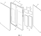
- FIG. 4 shows an unfolded structure of the foldable mobile phone 100. Referring to FIG. 4 , during folding, the mobile phone 100 may be folded along a broken line in FIG. 4 .
- the mobile phone 100 may include a flexible display 10, a middle frame 20, a circuit board 40, a battery 50, and a rear housing 30.
- the flexible display 10 and the rear housing 30 are separately located on two sides of the middle frame 20, and the circuit board 40 and the battery 50 may be located between the middle frame 20 and the rear housing 30 or the circuit board 40 and the battery 50 may be located between the middle frame 20 and the flexible display 10.
- the middle frame 20 may include a first middle frame 21 and a second middle frame 22.
- the first middle frame 21 and the second middle frame 22 are rotatably connected by using a rotating member 23 (for example, the rotating member 23 may be a rotating shaft, a hinge, or a flexible board).
- the rotating member 23 may be a rotating shaft, a hinge, or a flexible board.
- the first middle frame 21 and the second middle frame 22 may be metal middle frames.
- the first middle frame 21 and the second middle frame 22 may be middle frames made of two types of materials: ceramic and metal.
- edges of the first middle frame 21 and the second middle frame 22 are ceramic edges
- middle plates in the first middle frame 21 and the second middle frame 22 are metal middle plates
- the ceramic edges and the metal middle plates constitute the first middle frame 21 and the second middle frame 22.
- materials of the first middle frame 21 and the second middle frame 22 include but are not limited to metal and ceramic, and may be alternatively other materials.
- the first middle frame 21 and the second middle frame 22 may be folded horizontally along the broken line in FIG. 4 .
- the first middle frame 21 and the second middle frame 22 may be alternatively folded vertically, folded diagonally, or folded at any other angle.
- the mobile phone 100 shown in FIG. 5 includes two middle frames 20: the first middle frame 21 and the second middle frame 22, to fold two displays of the mobile phone 100.
- the mobile phone 100 may alternatively include three middle frames, so that three displays of the mobile phone 100 can be folded. A quantity of foldable displays of the mobile phone 100 is specifically set based on an actual requirement.
- one of the first middle frame 21 and the second middle frame 22 may be a middle frame corresponding to a main screen of the mobile phone 100, and the other may be a middle frame corresponding to a sub screen of the mobile phone 100.
- the first middle frame 21 may be a main middle frame corresponding to the main screen
- the second middle frame 22 may be a sub middle frame corresponding to the sub screen.
- the main screen and the sub screen of the mobile phone 100 are opposite to each other. In other words, after the mobile phone 100 is folded, both the front and the back of the mobile phone 100 are displays. In this case, a user may use the main screen for display, or may use the sub screen for display.
- the rear housing 30 when the mobile phone 100 includes the first middle frame 21 and the second middle frame 22, the rear housing 30 may be a rear housing 30 shown in FIG. 5 , and the rear housing 30 covers one side of the first middle frame 21 and the second middle frame 22.
- the rear housing 30 may be a flexible rear housing made of a flexible material.
- the rear housing 30 is a bendable flexible glass rear housing, or the rear housing 30 is a bendable plastic rear housing.
- the rear housing 30 may include a first rear housing and a second rear housing (not shown).
- the first rear housing is located on one side of the first middle frame 21, and the second rear housing is located on one side of the second middle frame 22; in other words, one rear housing is correspondingly disposed for each of the two middle frames.
- a bendable flexible substrate is used between the first rear housing and the second rear housing. In this way, during folding, the first rear housing and the second rear housing are folded around the flexible substrate.
- the first rear housing and the second rear housing may be metal rear housings, or the first rear housing and the second rear housing may be glass rear housings, or the first rear housing and the second rear housing may be ceramic rear housings. It should be noted that materials of the first rear housing and the second rear housing include but are not limited to metal, glass, or ceramic.
- the circuit board 40 may include a first circuit board 41 and a second circuit board 42.
- the first circuit board 41 and the second circuit board 42 may be electrically connected by using a flexible printed circuit (FPC).
- the first circuit board 41 may be located in the first middle frame 21, and the second circuit board 42 may be located in the second middle frame 22.
- One of the first circuit board 41 and the second circuit board 42 may be a main circuit board (namely, a mainboard), and the other may be a sub circuit board.
- the battery 50 may include a first battery 51 and a second battery 52.
- the first battery 51 may be located at a dashed-line position in the first middle frame 21 in FIG. 5
- the second battery 52 may be located at a dashed-line position in the second middle frame 22 in FIG. 5 .
- disposition positions of the first battery 51 and the second battery 52 include but are not limited to the dashed-line positions in the first middle frame 21 and the second middle frame 22 in FIG. 5 .
- the first battery 51 and the second battery 52 may be connected to a charging management module and the circuit board 40 by using a power management module.
- the power management module receives input from the battery 50 and/or the charging management module, and supplies power to a processor, an internal memory, an external memory, the flexible display 10, a camera, a communications module, and the like.
- the power management module may be further configured to monitor parameters such as a capacity of the battery 50, a cycle count of the battery 50, and a state of health (electric leakage and impedance) of the battery 50.
- the power management module may be disposed in the processor of the circuit board 40.
- the power management module and the charging management module may be alternatively disposed in a same component.
- the flexible display 10 may be an OLED display.
- the flexible display 10 When the mobile phone 100 is folded, the flexible display 10 may be bent along an arrow direction in FIG. 6 . After the folding, as shown in FIG. 7 , the flexible display 10 is bent at one end of the first middle frame 21 and the second middle frame 22. In this embodiment of this application, an end that is of the second middle frame 22 and that is away from the first middle frame 21 has an end cover 221. After the first middle frame 21 and the second middle frame 22 are folded, a width of a display area on the first middle frame 21 is less than a width of a display area on the second middle frame 22. In other words, after the mobile phone 100 is folded, the two displays differ in size.
- camera flashes 222 and a camera 223 may be disposed on the end cover 221.
- the end cover 221 may be fastened to the second middle frame 22 through clamping, welding, or integrated molding.
- the end cover 221 is disposed, so that the camera 223 and the camera flashes 222 can be disposed; and the user is not prone to contact with the display when holding the mobile phone 100, thereby facilitating the user in holding the mobile phone 100.
- a structure of the flexible display 10 may include a backplane 5, a display panel 4 disposed on the backplane 5, a touch panel 3, a polarizer 2, and a cover 1.
- the display panel 4 is connected to the touch panel 3 by using an adhesive layer 8b, and the touch panel 3 is connected to the polarizer 2 by using an adhesive layer 8a.
- the polarizer 2 is mainly used to increase screen brightness and is not necessary for display, and therefore can be omitted.
- a conventional touch panel 3 may include a support layer 3b and a touch layer 3a disposed on the support layer 3b.
- the support layer 3b in the touch panel 3 is connected to the display panel 4 by using the adhesive layer 8b, and the touch layer 3a in the touch panel 3 is connected to the polarizer 2 by using the adhesive layer 8a.
- Cyclo-olefin polymer Cyclo-olefin Polymer, COP is usually used as a material of the support layer 3b, and the COP material is relatively fragile.
- a stress on the COP material in a bending process is prone to exceed a material limit, and consequently the support layer 3b is prone to crack.
- an electrode layer of the touch layer 3a is prone to an open circuit due to cracking of the support layer 3b (because a part of the electrode layer of the touch layer 3a is patterned on the support layer 3b), causing a failure of some areas of the touch layer 3a.
- an embodiment of this application provides a flexible display 10, to reduce a risk that a touch layer in the flexible display 10 fails in a bending process.
- the following describes a structure of the flexible display 10 in the foldable mobile phone 100 for the following scenarios.
- the flexible display 10 may include a display panel 11, a first adhesive layer 12a, a touch film layer 13, a second adhesive layer 12b, and a polarizer 14 that are laminated sequentially.
- the first adhesive layer 12a is disposed between the display panel 11 and the touch film layer 13, and the second adhesive layer 12b is disposed between the touch film layer 13 and the polarizer 14.
- the first adhesive layer 12a is disposed on a light-emitting surface of the display panel 11
- the touch film layer 13 is fastened to the light-emitting surface of the display panel 11 by using the first adhesive layer 12a
- the second adhesive layer 12b is disposed on a surface that is of the touch film layer 13 and that faces the polarizer 14, and the polarizer 14 is fastened to the touch film layer 13 by using the second adhesive layer 12b.
- the light-emitting surface of the display panel 11 is a surface from which a light-emitting unit in the display panel 11 emits light.
- the display panel 11 emits light upward, in other words, the display panel 11 is top light-emitting, and therefore the light-emitting surface of the display panel 11 is a top surface of the display panel 11.
- the first adhesive layer 12a is disposed between the display panel 11 and the touch film layer 13. In this way, when the flexible display 10 is bent, the first adhesive layer 12a isolates a stress, to reduce a stress on the touch film layer 13 in a bending process, so that the touch film layer 13 is not prone to an open circuit risk in the bending process.
- the support layer 3b in the touch panel is removed. In this way, an overall thickness of the flexible display 10 is reduced, and a risk that an open circuit occurs on the touch film layer 13 because the support layer 3b is prone to crack is eliminated.
- the touch film layer 13 is disposed on the first adhesive layer 12a, and the first adhesive layer 12a isolates the stress for the touch film layer 13. In this way, the touch film layer 13 is not prone to an open circuit in the bending process, thereby ensuring normal use of the touch film layer 13.
- materials of the first adhesive layer 12a and the second adhesive layer 12b may be pressure sensitive adhesive (Pressure Sensitive Adhesive, PSA). During disposition, pressure sensitive adhesive may be compressed into a thin film in advance, and then the thin film is attached to the light-emitting surface of the display panel 11.
- materials of the first adhesive layer 12a and the second adhesive layer 12b may be optically clear adhesive (Optically Clear Adhesive, OCA), and optically clear adhesive may be disposed on the light-emitting surface of the display panel 11 through coating.
- adhesive layers made of pressure sensitive adhesive and the optically clear adhesive differ in thickness.
- the made adhesive layers each have a relatively large thickness; and when pressure sensitive adhesive is used as the materials of the first adhesive layer 12a and the second adhesive layer 12b, the made adhesive layers each have a relatively small thickness.
- pressure sensitive adhesive is used for the first adhesive layer 12a and the second adhesive layer 12b. In this way, it is ensured that the first adhesive layer 12a and the second adhesive layer 12b each have a relatively small thickness, thereby reducing the thickness of the flexible display 10.
- a thickness of each of the made first adhesive layer 12a and second adhesive layer 12b may be 50 to 100 ⁇ m.
- a thickness of each of the made first adhesive layer 12a and second adhesive layer 12b may be 15 to 25 ⁇ m.
- the thickness of each of the first adhesive layer 12a and the second adhesive layer 12b may be 18 ⁇ m, or the thickness of each of the first adhesive layer 12a and the second adhesive layer 12b may be 23 ⁇ m.
- the touch film layer 13 may include a lift-off layer 135 (Laser Lift-Off, LLO), a metal bridge layer 133 disposed on the lift-off layer 135, a first insulation layer 136 covering the lift-off layer 135 and the metal bridge layer 133, a first touch electrode 131 and a second touch electrode 132 that are patterned on the first insulation layer 136, and a second insulation layer 137 covering the first touch electrode 131, the second touch electrode 132, and the first insulation layer 136.
- LLO Lift-Off
- the first touch electrode 131 and the second touch electrode 132 cross, and the first touch electrode 131 and the second touch electrode 132 are insulated at a cross position.
- one of the first touch electrode 131 and the second touch electrode 132 is disconnected at the cross position.
- the first touch electrode 131 is disconnected at the cross position, and two disconnected ends of the first touch electrode 131 are both electrically connected to the metal bridge layer 133 by using via holes 134 disposed at the first insulation layer 136. In this way, two parts of the disconnected first touch electrode 131 are connected by using the metal bridge layer 133 and the via holes 134, so that the first touch electrode 131 and the second touch electrode 132 are insulated at the cross position.
- the first touch electrode 131 and the second touch electrode 132 may be disposed on the lift-off layer 135, and the metal bridge layer 133 may be disposed on the first insulation layer 136. In this way, the metal bridge layer 133 is located above the first touch electrode 131 and the second touch electrode 132.
- a position at which the metal bridge layer 133 is disposed includes but is limited to the position shown in FIG. 10 , provided that the metal bridge layer 133 can electrically connect two parts of a touch electrode disconnected at a cross position.
- one of the first touch electrode 131 and the second touch electrode 132 may be a drive electrode (Tx), and the other may be a receive electrode (Rx).
- the first touch electrode 131 may be a Tx
- the second touch electrode 132 may be an Rx.
- the first touch electrode 131, the second touch electrode 132, and the metal bridge layer 133 may be made of metal materials.
- the first touch electrode 131 and the second touch electrode 132 may be made of indium tin oxide (ITO) or may be made of indium zinc oxide (IZO), and a material of the metal bridge layer 133 may be copper metal or silver.
- a metal material of the via hole may be silver paste.
- the first insulation layer 136 and the second insulation layer 137 may be organic insulation layers.
- a material of the lift-off layer 135 may be polyimide (Polyimide, PI). It should be noted that materials of the first touch electrode 131, the second touch electrode 132, the metal bridge layer 133, the first insulation layer 136, the second insulation layer 137, and the lift-off layer 135 include but are not limited to the foregoing materials.
- the material of the lift-off layer 135 may be polyimide (Polyimide, PI).
- the first adhesive layer 12a and the lift-off layer 135 are both organic film layers and therefore have a same attribute. Therefore, when the display panel 11 is adhered to the lift-off layer 135 in the touch film layer 13 by using the first adhesive layer 12a, an adhesive force between the first adhesive layer 12a and the lift-off layer 135 is greater, so that an adhesive force between the display panel 11 and the touch film layer 13 is greater, and the display panel 11 is not prone to lift off from the touch film layer 13 in the bending process.
- the polarizer 14 is adhered to the second insulation film layer in the touch film layer 13 by using the second adhesive layer 12b.
- the second insulation layer 137 and the second adhesive layer 12b are both organic film layers and therefore have a same attribute. Therefore, an adhesive force between the second adhesive layer 12b and the second insulation film layer is greater, so that an adhesive force between the polarizer 14 and the touch film layer 13 is greater, and the polarizer 14 is not prone to lift off from the touch film layer 13 in the bending process.
- a thickness of the touch film layer 13 may be 6 to 15 ⁇ m.
- the thickness of the touch film layer 13 may be 7 ⁇ m, or the thickness of the touch film layer 13 may be 10 ⁇ m.
- a thickness of the lift-off layer 135 may be 2 to 5 ⁇ m.
- the thickness of the lift-off layer 135 may be 3 ⁇ m.
- a thickness of the metal bridge layer 133 may be 0.1 to 0.4 ⁇ m.
- the thickness of the metal bridge layer 133 may be 0.2 ⁇ m.
- a thickness of the first insulation layer 136 may be 1.0 to 2 ⁇ m.
- the thickness of the first insulation layer 136 may be 1.8 ⁇ m.
- a thickness of each of the first touch electrode 131 and the second touch electrode 132 may be 0.07 to 0.1 ⁇ m.
- the thickness of each of the first touch electrode 131 and the second touch electrode 132 may be 0.08 ⁇ m.
- a thickness of the second insulation layer 137 may be 1.0 to 2 ⁇ m.
- the thickness of the second insulation layer 137 may be 1.8 ⁇ m.
- the touch film layer 13 is provided.
- the lift-off layer 135 LLO
- a material of the substrate 130 may be cyclo-olefin polymer (COP).
- the metal bridge layer 133 is formed on the lift-off layer 135, the lift-off layer 135 and the metal bridge layer 133 are covered with the first insulation layer 136, via holes electrically connected to the metal bridge layer 133 are formed in the first insulation layer 136, the patterned first touch electrode 131 and second touch electrode 132 are formed on the first insulation layer 136, the first touch electrode 131 is electrically connected to the metal bridge layer 133 by using the via hole 134, and the first insulation layer 136, the first touch electrode 131, and the second touch electrode 132 are covered with the second insulation layer 137 to form a touch panel.
- the touch panel is irradiated by using a laser. Under the action of the laser, a hydrogen bond force between the lift-off layer 135 and the substrate 130 is destroyed.
- the substrate 130 lifts off from the lift-off layer 135 along a dashed line in FIG. 11 , to obtain the touch film layer 13.
- the polarizer 14 is fastened to the second insulation layer 137 in the touch film layer 13 by using the second adhesive layer 12b.
- the display panel 11 is fastened to the lift-off layer 135 in the touch film layer 13 (for example, is fastened to a surface that is of the lift-off layer 135 and that is opposite to the metal bridge layer 133) by using the first adhesive layer 12a, to form the flexible display 10.
- a sequence of fastening the polarizer 14 and the display panel 11 to the touch film layer 13 includes but is not limited to the sequence, shown in FIG. 11 , in which the polarizer 14 is first fastened and then the display panel 11 is fastened.
- the display panel 11 may be first fastened to the lift-off layer 135 by using the first adhesive layer 12a, and then the polarizer 14 may be fastened to the second insulation layer 137 by using the second adhesive layer 12b.
- the flexible display 10 may further include a protective layer, and the protective layer may include a first protective layer 16 and a second protective layer 17.
- the first protective layer 16 is fastened to the polarizer 14 by using a third adhesive layer 12c
- the second protective layer 17 is fastened to the first protective layer 16 by using a fourth adhesive layer 12d.
- Materials of the first protective layer 16 and the second protective layer 17 may be PI.
- a material of the first protective layer 16 may be PI
- the second protective layer 17 may be a flexible hard coat (Hard Coat, HC)
- materials of the third adhesive layer 12c and the fourth adhesive layer 12d may be optically clear adhesive (OCA) or may be pressure sensitive adhesive (PSA).
- the display panel 11 may be an OLED display panel.
- the display panel 11 may include a flexible substrate 111, a back film 113, and a display layer 115.
- a fifth adhesive layer 112 is disposed on the flexible substrate 111, the back film 113 is fastened to the flexible substrate 111 by using the fifth adhesive layer 112, a sixth adhesive layer 114 is disposed on a surface that is of the back film 113 and that faces the display layer 115, and the display layer 115 is fastened to the back film 113 by using the sixth adhesive layer 114.
- the display layer 115 is adhered to the lift-off layer 135 by using the first adhesive layer 12a.
- the display layer 115 may include a thin film transistor (Thin Film Transistor, TFT) layer and the light-emitting unit (not shown).
- the light-emitting unit may include a cathode, an anode, and a plurality of organic light-emitting layers (not shown) disposed between the cathode and the anode.
- the flexible substrate 111 plays a support role, and the back film 113 protects the display layer 115.
- a material of the back film 113 may include but is not limited to PI, and materials of the fifth adhesive layer 112 and the sixth adhesive layer 114 may be optically clear adhesive (OCA) or may be pressure sensitive adhesive (PSA).
- OCA optically clear adhesive
- PSA pressure sensitive adhesive
- the flexible display 10 may further include an adjustment layer 15.
- the adjustment layer 15 is located between the touch film layer 13 and the first adhesive layer 12a.
- the touch film layer 13 is disposed on one surface of the adjustment layer 15, and the other surface of the adjustment layer 15 is fastened to the display panel 11 by using the first adhesive layer 12a.
- the adjustment layer 15 is included, and the adjustment layer 15 may serve as a neutral layer for adjusting bending of the flexible display 10, to reduce a stress on the touch film layer 13 during bending, so that the touch film layer 13 is not prone to crack in a bending process.
- a matching degree of temperature and humidity deformation systems of upper and lower layers of the touch film layer 13 may be adjusted by using the adjustment layer 15, to reduce a risk that the touch film layer 13 cracks due to an internal stress when the touch film layer 13 is bent at temperature and humidity.
- the flexible display 10 includes the adjustment layer 15, impact resistance capabilities of the flexible display 10 are increased. In this way, after the flexible display 10 is unfolded, the flexible display 10 is not prone to crack in vertical and horizontal directions under a condition such as an external impact. Therefore, the adjustment layer 15 is disposed, so that the impact resistance capabilities of the flexible display 10 in the vertical and horizontal directions during unfolding are increased.
- the adjustment layer 15 may include a first adjustment layer 15a and a second adjustment layer 15b.
- the first adjustment layer 15a is located between the second adjustment layer 15b and the first adhesive layer 12a
- the second adjustment layer 15b is located between the touch film layer 13 and the first adjustment layer 15a.
- the touch film layer 13 is disposed on the second adjustment layer 15b
- the second adjustment layer 15b is located on the first adjustment layer 15a
- the first adjustment layer 15a is located on the first adhesive layer 12a.
- the second adjustment layer 15b may isolate a stress for the touch film layer 13, to reduce a stress on the touch film layer 13 during bending (as shown in FIG. 14 ).
- the second adjustment layer 15b may be a glue layer, for example, may be made of pressure sensitive adhesive (PSA) or optically clear adhesive (OCA). In this way, the second adjustment layer 15b may further adhere the touch film layer 13 to the first adjustment layer 15a. Therefore, in this embodiment of this application, when the second adjustment layer 15b is a glue layer, the second adjustment layer 15b isolates the stress for the touch film layer 13, and fastens the touch film layer 13 to the first adjustment layer 15a.
- PSA pressure sensitive adhesive
- OCA optically clear adhesive
- a material of the first adjustment layer 15a may be an optical material.
- the optical material may include but is not limited to cyclo-olefin polymer (COP) or polyethylene terephthalate (Polyethylene terephthalate, PET).
- COP has relatively good light transmission performance. Therefore, in this embodiment of this application, the first adjustment layer 15a is a COP layer.
- the first adjustment layer 15a is made of COP, the touch film layer 13 and the first adjustment layer 15a are separated by the second adjustment layer 15b. Therefore, compared with the flexible display in FIG. 8 , in this embodiment of this application, the second adjustment layer 15b separates the touch film layer 13 from the COP layer (namely, the first adjustment layer 15a). In this way, the touch electrode in the touch film layer 13 is not prone to an open circuit when the COP layer cracks.
- the first adjustment layer 15a and the second adjustment layer 15b are disposed between the touch film layer 13 and the display panel 11. In this way, a distance between the touch film layer 13 and the display panel 11 increases, so that noise of a cathode layer in the display panel 11 is prevented from interfering with the touch film layer 13, thereby avoiding crosstalk between the touch film layer 13 and the display panel 11.
- the first adjustment layer 15a and the second adjustment layer 15b are disposed. Therefore, first, a stress adjustment role is implemented, to reduce the stress on the touch film layer 13 during bending; second, a matching degree of temperature and humidity deformation coefficients of the touch film layer 13 is adjusted; third, the impact resistance capabilities of the flexible display 10 in the vertical and horizontal directions during unfolding are increased; and fourth, the crosstalk between the touch film layer 13 and the display panel 11 is avoided.
- first adjustment layer 15a when the first adjustment layer 15a is a COP layer and the second adjustment layer 15b is a PSA layer, material Young's moduli of the first adjustment layer 15a and the second adjustment layer 15b are shown in Table 1.
- Table 1 Material model Young's modulus Second adjustment layer 15b: PSA 1# 800 kPa Second adjustment layer 15b: PSA 2# 150 kPa Second adjustment layer 15b: PSA 3# 22 kPa Second adjustment layer 15b: PSA 4# 80 kPa
- First adjustment layer 15a COP 2.0 GPa
- the first adjustment layer 15a is a COP layer and the second adjustment layer 15b is a PSA layer
- a Young's modulus of the first adjustment layer 15a is greater than a Young's modulus of the second adjustment layer 15b, and therefore the first adjustment layer 15a is a high Young's modulus layer and the second adjustment layer 15b is a low Young's modulus layer.
- a structure including the high Young's modulus layer and the low Young's modulus layer is added between the touch film layer 13 and the display panel 11, to adjust a stress state of the touch film layer 13 to match the temperature and humidity coefficients of the upper and lower layers of the touch film layer 13, thereby improving structural strength of the flexible display 10.
- a thickness h1 of the first adjustment layer 15a may be 20 to 40 ⁇ m.
- the thickness h1 of the first adjustment layer 15a may be 23 ⁇ m, or the thickness h1 of the first adjustment layer 15a may be 30 ⁇ m.
- a thickness h2 of the second adjustment layer 15b may be 15 to 25 ⁇ m.
- the thickness h2 of the second adjustment layer 15b may be 18 ⁇ m, or the thickness h2 of the second adjustment layer 15b may be 20 ⁇ m.
- the lift-off layer 135 in the touch film layer 13 is located on the second adjustment layer 15b.
- the lift-off layer 135 is fastened to the first adjustment layer 15a by using the second adjustment layer 15b.
- the lift-off layer 135 and the first adjustment layer 15a are both organic film layers.
- the touch film layer 13 may be provided.
- the lift-off layer 135 LLO
- a material of the substrate 130 may be cyclo-olefin polymer (COP).
- the metal bridge layer 133 is formed on the lift-off layer 135, the lift-off layer 135 and the metal bridge layer 133 are covered with the first insulation layer 136, via holes electrically connected to the metal bridge layer 133 are formed in the first insulation layer 136, the patterned first touch electrode 131 and second touch electrode 132 are formed on the first insulation layer 136, the first touch electrode 131 is electrically connected to the metal bridge layer 133 by using the via hole 134, and the first insulation layer 136, the first touch electrode 131, and the second touch electrode 132 are covered with the second insulation layer 137 to form a touch panel.
- the touch panel is irradiated by using a laser. Under the action of the laser, a hydrogen bond force between the lift-off layer 135 and the substrate 130 is destroyed.
- the substrate 130 lifts off from the lift-off layer 135 along a dashed line in FIG. 16 , to obtain the touch film layer 13.
- the polarizer 14 is fastened to the second insulation layer 137 in the touch film layer 13 by using the second adhesive layer 12b.
- the second adjustment layer 15b is made of PSA, and therefore the first adjustment layer 15a is fastened to the lift-off layer 135 (for example, is fastened to a surface that is of the lift-off layer 135 and that faces the display panel 11) by using the second adjustment layer 15b.
- the display panel 11 is fastened to the first adjustment layer 15a (for example, is fastened to a surface that is of the first adjustment layer 15a and that faces the display panel 11) by using the first adhesive layer 12a, to form the flexible display 10.
- a sequence of disposing the touch film layer 13, the polarizer 14, the display panel 11, and the adjustment layer 15 includes but is not limited to the preparation sequence shown in FIG. 11 .
- the adjustment layer 15 may be fastened to the display panel 11 by using the first adhesive layer 12a, and then a structure formed by the display panel 11 and the adjustment layer 15 is fastened to the lift-off layer 135 by using the first adjustment layer 15a; and the polarizer 14 is fastened to the second insulation layer 137 in the touch film layer 13 by using the second adhesive layer 12b.
- the flexible display 10 may further include a first protective layer 16 and a second protective layer 17.
- first protective layer 16 is fastened to the polarizer 14 by using a third adhesive layer 12c
- second protective layer 17 is fastened to the first protective layer 16 by using a fourth adhesive layer 12d.
- Materials of the first protective layer 16 and the second protective layer 17 may be PI.
- a material of the first protective layer 16 may be PI
- the second protective layer 17 may be a flexible hard coat (Hard Coat, HC)
- materials of the third adhesive layer 12c and the fourth adhesive layer 12d may be optically clear adhesive (OCA) or may be pressure sensitive adhesive (PSA).
- OCA optically clear adhesive
- PSA pressure sensitive adhesive
- the display panel 11 may be an OLED display panel 11.
- the display panel 11 may include a flexible substrate 111, a back film 113, and a display layer 115.
- a fifth adhesive layer 112 is disposed on the flexible substrate 111
- the back film 113 is fastened to the flexible substrate 111 by using a sixth adhesive layer 114
- a sixth adhesive layer 114 is disposed on a surface that is of the back film 113 and that faces the display layer 115
- the display layer 115 is fastened to the back film 113 by using the sixth adhesive layer 114.
- the display layer 115 is adhered to the lift-off layer 135 by using the first adhesive layer 12a.
- the display layer 115 may include a thin film transistor (Thin Film Transistor, TFT) layer and the light-emitting unit.
- the light-emitting unit may include a cathode, an anode, and a plurality of organic light-emitting layers disposed between the cathode and the anode.
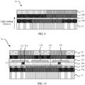
- a simulation test is performed on maximum principal strains (there is a positive correlation between a maximum principal strain and a stress, for example, a greater maximum principal strain indicates a greater stress) of each film layer in the flexible display 10 in the scenario 1 and the scenario 2 during bending.
- a test result is shown in FIG. 18 and FIG. 19 .
- the second protective layer 17 is made of PI
- the fourth adhesive layer 12d is made of OCA
- the first protective layer 16 is made of PI
- the third adhesive layer 12c is made of OCA
- the polarizer 14 is a circular polarizer 14
- the second adhesive layer 12b is made of PSA
- the second adjustment layer 15b is made of PSA (with a Young's modulus of 800 kPa)
- the first adjustment layer 15a is made of COP
- the first adhesive layer 12a is made of PSA
- the sixth adhesive layer 114 is made of OCA
- the back film 113 is made of PI
- the fifth adhesive layer 112 is made of OCA.
- each adhesive layer suffers a greater stress.
- a stress on each adhesive layer in the scenario 2 is less than a stress on each adhesive layer in the scenario 1. Therefore, in the scenario 2, the adjustment layer 15 is disposed, and the adjustment layer 15 serves as a neutral layer for bending adjustment, to reduce the stress on each adhesive layer.
Landscapes
- Engineering & Computer Science (AREA)
- Theoretical Computer Science (AREA)
- Physics & Mathematics (AREA)
- General Engineering & Computer Science (AREA)
- General Physics & Mathematics (AREA)
- Computer Hardware Design (AREA)
- Human Computer Interaction (AREA)
- Microelectronics & Electronic Packaging (AREA)
- Nonlinear Science (AREA)
- Mathematical Physics (AREA)
- Chemical & Material Sciences (AREA)
- Crystallography & Structural Chemistry (AREA)
- Optics & Photonics (AREA)
- Devices For Indicating Variable Information By Combining Individual Elements (AREA)
- Electroluminescent Light Sources (AREA)
Applications Claiming Priority (2)
| Application Number | Priority Date | Filing Date | Title |
|---|---|---|---|
| CN201910823881.XA CN112447792A (zh) | 2019-09-02 | 2019-09-02 | 一种柔性显示屏及其制备方法和电子设备 |
| PCT/CN2020/112990 WO2021043159A1 (fr) | 2019-09-02 | 2020-09-02 | Écran d'affichage flexible, son procédé de préparation et dispositif électronique |
Publications (2)
| Publication Number | Publication Date |
|---|---|
| EP4020576A1 true EP4020576A1 (fr) | 2022-06-29 |
| EP4020576A4 EP4020576A4 (fr) | 2023-05-31 |
Family
ID=74735009
Family Applications (1)
| Application Number | Title | Priority Date | Filing Date |
|---|---|---|---|
| EP20861229.1A Withdrawn EP4020576A4 (fr) | 2019-09-02 | 2020-09-02 | Écran d'affichage flexible, son procédé de préparation et dispositif électronique |
Country Status (4)
| Country | Link |
|---|---|
| US (1) | US20220261039A1 (fr) |
| EP (1) | EP4020576A4 (fr) |
| CN (1) | CN112447792A (fr) |
| WO (1) | WO2021043159A1 (fr) |
Cited By (2)
| Publication number | Priority date | Publication date | Assignee | Title |
|---|---|---|---|---|
| US11941209B2 (en) | 2020-06-24 | 2024-03-26 | Boe Technology Group Co., Ltd. | Touch module, preparation method therefor, and display device |
| EP4287170A4 (fr) * | 2022-04-18 | 2024-07-03 | Honor Device Co., Ltd. | Appareil d'affichage pliable et procédé de fabrication associé, et dispositif terminal |
Families Citing this family (6)
| Publication number | Priority date | Publication date | Assignee | Title |
|---|---|---|---|---|
| CN113452814A (zh) * | 2021-05-21 | 2021-09-28 | 荣耀终端有限公司 | 传输组件及可折叠电子设备 |
| KR102954237B1 (ko) * | 2021-07-29 | 2026-04-20 | 삼성디스플레이 주식회사 | 표시 장치 |
| CN113972349B (zh) * | 2021-10-19 | 2022-11-29 | 京东方科技集团股份有限公司 | 显示面板及其制造方法 |
| WO2023142014A1 (fr) | 2022-01-29 | 2023-08-03 | 京东方科技集团股份有限公司 | Panneau d'affichage tactile, dispositif d'affichage tactile et carte mère d'affichage tactile |
| CN218477123U (zh) * | 2022-11-04 | 2023-02-14 | 赵芝君 | 屏幕保护组件及电子设备 |
| CN117012101A (zh) * | 2023-08-22 | 2023-11-07 | 厦门天马显示科技有限公司 | 显示模组及其制作方法、显示装置 |
Family Cites Families (12)
| Publication number | Priority date | Publication date | Assignee | Title |
|---|---|---|---|---|
| US9417746B2 (en) * | 2012-02-09 | 2016-08-16 | Sharp Kabushiki Kaisha | Touch-panel substrate |
| KR102080011B1 (ko) * | 2013-06-13 | 2020-02-24 | 삼성디스플레이 주식회사 | 표시장치 및 그 제조방법 |
| KR102319835B1 (ko) * | 2014-09-22 | 2021-11-01 | 엘지디스플레이 주식회사 | 접이식 디스플레이 장치 |
| KR102438786B1 (ko) * | 2015-10-13 | 2022-08-31 | 코닝 인코포레이티드 | 가요성 전자 장치 모듈들, 물품들 및 그의 제조 방법들 |
| CN106024840A (zh) * | 2016-07-12 | 2016-10-12 | 上海天马微电子有限公司 | 柔性oled显示面板及其制作方法、柔性oled显示装置 |
| CN106558279B (zh) * | 2017-01-13 | 2019-05-14 | 京东方科技集团股份有限公司 | 柔性显示装置及其制备方法 |
| CN108461519A (zh) * | 2017-02-21 | 2018-08-28 | 京东方科技集团股份有限公司 | 柔性显示面板及其制备方法、显示装置 |
| KR102057065B1 (ko) * | 2017-02-23 | 2019-12-18 | 동우 화인켐 주식회사 | 편광층 및 터치 센서 일체형 광학 적층체 및 이를 포함하는 화상 표시 장치 |
| KR102117568B1 (ko) * | 2017-02-28 | 2020-06-01 | 동우 화인켐 주식회사 | 윈도우 기판 및 이를 포함하는 화상 표시 장치 |
| KR102505265B1 (ko) * | 2017-06-23 | 2023-03-06 | 삼성디스플레이 주식회사 | 전자 장치 |
| KR102391396B1 (ko) * | 2017-09-28 | 2022-04-26 | 엘지디스플레이 주식회사 | 플렉서블 표시장치용 편광판 및 이를 포함하는 플렉서블 표시장치 |
| CN109659333A (zh) * | 2017-10-11 | 2019-04-19 | 上海和辉光电有限公司 | 抗反射阻水氧组件及其制造方法、柔性显示器件 |
-
2019
- 2019-09-02 CN CN201910823881.XA patent/CN112447792A/zh active Pending
-
2020
- 2020-09-02 US US17/630,558 patent/US20220261039A1/en not_active Abandoned
- 2020-09-02 WO PCT/CN2020/112990 patent/WO2021043159A1/fr not_active Ceased
- 2020-09-02 EP EP20861229.1A patent/EP4020576A4/fr not_active Withdrawn
Cited By (2)
| Publication number | Priority date | Publication date | Assignee | Title |
|---|---|---|---|---|
| US11941209B2 (en) | 2020-06-24 | 2024-03-26 | Boe Technology Group Co., Ltd. | Touch module, preparation method therefor, and display device |
| EP4287170A4 (fr) * | 2022-04-18 | 2024-07-03 | Honor Device Co., Ltd. | Appareil d'affichage pliable et procédé de fabrication associé, et dispositif terminal |
Also Published As
| Publication number | Publication date |
|---|---|
| CN112447792A (zh) | 2021-03-05 |
| US20220261039A1 (en) | 2022-08-18 |
| WO2021043159A1 (fr) | 2021-03-11 |
| EP4020576A4 (fr) | 2023-05-31 |
Similar Documents
| Publication | Publication Date | Title |
|---|---|---|
| US20220261039A1 (en) | Flexible display and preparation method thereof, and electronic device | |
| US11096274B2 (en) | Flexible display device | |
| US10613697B2 (en) | Touch panel and manufacturing method therefor | |
| CN109817684B (zh) | 柔性oled模组堆叠结构及其制备方法 | |
| CN205485162U (zh) | 显示装置 | |
| WO2014025534A1 (fr) | Dispositifs d'affichage flexibles | |
| CN111064829B (zh) | 一种显示装置及终端设备 | |
| US10416509B2 (en) | Display panel, electronic device, and display panel fabrication method | |
| US20160219354A1 (en) | Speaker and microphone integrated display panel | |
| CN103268168A (zh) | 触控显示模块 | |
| CN112017535A (zh) | 显示设备 | |
| TWI244057B (en) | Dual display module | |
| KR102236034B1 (ko) | 유연성 디스플레이 장치 | |
| CN105572929A (zh) | 显示面板及其制备方法、显示装置 | |
| US20130329350A1 (en) | Electronic apparatus | |
| EP4716439A1 (fr) | Dispositif d'affichage, dispositif électronique le comprenant et procédé de fabrication de dispositif d'affichage | |
| CN103533758B (zh) | 软性线路板的制作方法 | |
| CN112766198A (zh) | 显示模组及电子设备 | |
| CN118280224A (zh) | 显示模组 | |
| CN118262621A (zh) | 电子装置和制造电子装置的方法 | |
| CN114882802A (zh) | 一种显示模组和电子设备 | |
| KR20120068108A (ko) | 판상도전기판 및 그를 이용한 전기 장치 |
Legal Events
| Date | Code | Title | Description |
|---|---|---|---|
| STAA | Information on the status of an ep patent application or granted ep patent |
Free format text: STATUS: THE INTERNATIONAL PUBLICATION HAS BEEN MADE |
|
| PUAI | Public reference made under article 153(3) epc to a published international application that has entered the european phase |
Free format text: ORIGINAL CODE: 0009012 |
|
| STAA | Information on the status of an ep patent application or granted ep patent |
Free format text: STATUS: REQUEST FOR EXAMINATION WAS MADE |
|
| 17P | Request for examination filed |
Effective date: 20220324 |
|
| AK | Designated contracting states |
Kind code of ref document: A1 Designated state(s): AL AT BE BG CH CY CZ DE DK EE ES FI FR GB GR HR HU IE IS IT LI LT LU LV MC MK MT NL NO PL PT RO RS SE SI SK SM TR |
|
| DAV | Request for validation of the european patent (deleted) | ||
| DAX | Request for extension of the european patent (deleted) | ||
| REG | Reference to a national code |
Ref country code: DE Ref legal event code: R079 Free format text: PREVIOUS MAIN CLASS: H01L0027320000 Ipc: G06F0001160000 |
|
| RIC1 | Information provided on ipc code assigned before grant |
Ipc: G06F 1/16 20060101AFI20230126BHEP |
|
| A4 | Supplementary search report drawn up and despatched |
Effective date: 20230504 |
|
| RIC1 | Information provided on ipc code assigned before grant |
Ipc: G06F 1/16 20060101AFI20230427BHEP |
|
| STAA | Information on the status of an ep patent application or granted ep patent |
Free format text: STATUS: EXAMINATION IS IN PROGRESS |
|
| 17Q | First examination report despatched |
Effective date: 20241011 |
|
| STAA | Information on the status of an ep patent application or granted ep patent |
Free format text: STATUS: THE APPLICATION IS DEEMED TO BE WITHDRAWN |
|
| 18D | Application deemed to be withdrawn |
Effective date: 20250212 |