EP4024293A1 - Quantenmess- und -steuersystem für multi-bit-quantenrückkopplungssteuerung - Google Patents
Quantenmess- und -steuersystem für multi-bit-quantenrückkopplungssteuerung Download PDFInfo
- Publication number
- EP4024293A1 EP4024293A1 EP21759007.4A EP21759007A EP4024293A1 EP 4024293 A1 EP4024293 A1 EP 4024293A1 EP 21759007 A EP21759007 A EP 21759007A EP 4024293 A1 EP4024293 A1 EP 4024293A1
- Authority
- EP
- European Patent Office
- Prior art keywords
- mcsg
- control
- quantum
- physical
- node
- Prior art date
- Legal status (The legal status is an assumption and is not a legal conclusion. Google has not performed a legal analysis and makes no representation as to the accuracy of the status listed.)
- Pending
Links
Images



Classifications
-
- H—ELECTRICITY
- H04—ELECTRIC COMMUNICATION TECHNIQUE
- H04L—TRANSMISSION OF DIGITAL INFORMATION, e.g. TELEGRAPHIC COMMUNICATION
- H04L7/00—Arrangements for synchronising receiver with transmitter
- H04L7/02—Speed or phase control by the received code signals, the signals containing no special synchronisation information
- H04L7/033—Speed or phase control by the received code signals, the signals containing no special synchronisation information using the transitions of the received signal to control the phase of the synchronising-signal-generating means, e.g. using a phase-locked loop
-
- G—PHYSICS
- G06—COMPUTING OR CALCULATING; COUNTING
- G06N—COMPUTING ARRANGEMENTS BASED ON SPECIFIC COMPUTATIONAL MODELS
- G06N10/00—Quantum computing, i.e. information processing based on quantum-mechanical phenomena
- G06N10/20—Models of quantum computing, e.g. quantum circuits or universal quantum computers
-
- G—PHYSICS
- G06—COMPUTING OR CALCULATING; COUNTING
- G06N—COMPUTING ARRANGEMENTS BASED ON SPECIFIC COMPUTATIONAL MODELS
- G06N10/00—Quantum computing, i.e. information processing based on quantum-mechanical phenomena
-
- G—PHYSICS
- G06—COMPUTING OR CALCULATING; COUNTING
- G06N—COMPUTING ARRANGEMENTS BASED ON SPECIFIC COMPUTATIONAL MODELS
- G06N10/00—Quantum computing, i.e. information processing based on quantum-mechanical phenomena
- G06N10/40—Physical realisations or architectures of quantum processors or components for manipulating qubits, e.g. qubit coupling or qubit control
-
- G—PHYSICS
- G06—COMPUTING OR CALCULATING; COUNTING
- G06N—COMPUTING ARRANGEMENTS BASED ON SPECIFIC COMPUTATIONAL MODELS
- G06N10/00—Quantum computing, i.e. information processing based on quantum-mechanical phenomena
- G06N10/70—Quantum error correction, detection or prevention, e.g. surface codes or magic state distillation
-
- H—ELECTRICITY
- H04—ELECTRIC COMMUNICATION TECHNIQUE
- H04L—TRANSMISSION OF DIGITAL INFORMATION, e.g. TELEGRAPHIC COMMUNICATION
- H04L45/00—Routing or path finding of packets in data switching networks
- H04L45/40—Wormhole routing
-
- B—PERFORMING OPERATIONS; TRANSPORTING
- B82—NANOTECHNOLOGY
- B82Y—SPECIFIC USES OR APPLICATIONS OF NANOSTRUCTURES; MEASUREMENT OR ANALYSIS OF NANOSTRUCTURES; MANUFACTURE OR TREATMENT OF NANOSTRUCTURES
- B82Y10/00—Nanotechnology for information processing, storage or transmission, e.g. quantum computing or single electron logic
-
- H—ELECTRICITY
- H04—ELECTRIC COMMUNICATION TECHNIQUE
- H04L—TRANSMISSION OF DIGITAL INFORMATION, e.g. TELEGRAPHIC COMMUNICATION
- H04L49/00—Packet switching elements
- H04L49/25—Routing or path finding in a switch fabric
- H04L49/251—Cut-through or wormhole routing
Definitions
- Embodiments of the present disclosure relate to the field of quantum technologies, and in particular, to a quantum measurement and control (QMC) system for multi-bit quantum feedback control.
- QMC quantum measurement and control
- a quantum chip is a core processing part of a quantum computer.
- a QMC system may need to to measure a quantum state of the each qubit on the quantum chip and run a quantum error correction (QEC) algorithm to perform error correction control on an erroneous qubit.
- QEC quantum error correction
- Embodiments of the present disclosure provide a QMC system for multi-bit quantum feedback control.
- the technical solutions are as follows:
- a QMC system for multi-bit quantum feedback control includes a measurement and control (MC) network including a plurality of measurement and control subgroups (MCSGs), each MCSG being used as a node in the MC network and having a connection relationship with at least one another MCSG;
- MC measurement and control
- MCSGs measurement and control subgroups
- a group of physical qubits share a set of hardware of an MC system by setting up an MCSG.
- a measurement unit in the MCSG directly generates an error correction code in the group and distributes feedback control signals to control units in the group, to implement quick feedback, thereby reducing an amount of communication between physical boards.
- a quantum operation on a superconducting quantum chip (SCQC) has a spatial locality, and the measurement unit in the MCSG can forward more measurement results of this group to other adjacent MCSGs with a lower delay. Setting up the MCSG may minimize a communication delay of a system network and a running time of a QEC algorithm.
- Cloud technology is a hosting technology that gathers a series of resources such as hardware, software, and networks in a wide area network or a local area network to implement computing, storage, processing, and sharing of data.
- the cloud technology is a generic term for a network technology, an information technology, an integration technology, a management platform technology, an application technology, and the like based on an application of a cloud computing business mode.
- a resource pool may be formed, and resources are used based on a requirement, which is flexible and convenient.
- a cloud computing technology becomes an important support.
- a backend service of a technical network system requires a large amount of computing and storage resources, such as a video website, an image website, and more portal websites.
- each article may have its own identifier in the future, which may need to be transmitted to a backend system for logical processing. Data at different levels is separately processed, and data in various industries requires strong system support, which can be implemented through cloud computing.
- the cloud technology involves basic technologies such as cloud computing, cloud storage, databases, and big data.
- Cloud applications provided based on the cloud technology include medical cloud, cloud IoT, cloud security, cloud calling, private cloud, public cloud, hybrid cloud, cloud gaming, cloud education, cloud conference, cloud social, artificial intelligence cloud services, and the like.
- a system based on a cloud technology includes a server and a terminal.
- the server may be an independent physical server, or may be a server cluster or a distributed system including a plurality of physical servers, or may be a cloud server that provides a basic cloud computing service such as a cloud service, a cloud database, cloud computing, a cloud function, cloud storage, a network service, cloud communication, a middleware service, a domain name service, a security service, a content delivery network (CDN), big data, and an artificial intelligence platform.
- the terminal may be a smartphone, a tablet computer, a notebook computer, a desktop computer, a smart speaker, a smartwatch, or the like, but is not limited thereto.
- the terminal and the server may be directly or indirectly connected in a wired or wireless communication manner. This is not limited in this embodiment of the present disclosure.
- a quantum computer is a machine that uses the principles of quantum mechanics to perform computations. Based on a superposition principle and quantum entanglement of the quantum mechanics, the quantum computer has a strong parallel processing capability and can resolve some problems that are difficult for a classical computer to compute. Because of a zero-resistance characteristic of a superconducting quantum bit (SC qubit) and a manufacturing process close to that of an integrated circuit, a quantum computing (QC) system constructed using the SC qubit is one of the most promising systems for implementing practical QC.
- SC qubit superconducting quantum bit
- QC quantum computing
- a quantum processor refers to a quantum-level computer processor, that is, a processor of a quantum computer.
- the quantum processor may include one or more quantum chips.
- the quantum chip (or an SCQC) is a central processing unit of the quantum computer and is a core part of the quantum computer.
- the quantum chip integrates quantum circuits on a substrate, to carry a function of quantum information processing. Drawing lessons from the development of a conventional computer, after overcoming the bottleneck technology in quantum computer research, it may be necessary to move onto integration to achieve commercialization and industrial upgrading.
- a superconducting system, a semiconductor quantum dot system, a micro-nano photonics system, and even an atomic and ion system are all expected to move onto chips.
- an SCQC system is technically ahead of other physical systems, and the conventional semiconductor quantum dot system is also an objective that people try to explore, because the development of the conventional semiconductor industry is already mature, for example, once a semiconductor quantum chip breaks a threshold of fault-tolerance quantum computing (FTQC) in terms of decoherence time and manipulation accuracy, it is expected to integrate existing achievements of the conventional semiconductor industry to reduce development costs.
- FTQC fault-tolerance quantum computing
- a system constructed based on a cloud technology in the future can use the quantum computer to perform some processing and computations to provide better services.
- a scalable SCQC has reached a range of 50-100 bits.
- a Sycamore architecture of Google as an example, a plurality of qubits are arranged by using a two-dimensional structure. Each qubit and a quantum coupler between bits may need to be controlled by an independent microwave pulse signal. Measurement of a quantum state of the qubit mostly adopts a dispersive readout manner, and each combined pulse measurement signal transmitted by a measurement device can simultaneously read states of a plurality of qubits.
- QEC is a foundation of universal QC.
- a surface code error correction method that is mature in theory depends on measurement of a logical qubit including a group of physical qubits, and performs feedback control on a measured or adjacent physical bit according to a measurement result.
- a QMC system may need to meet the following requirements.
- the QMC system may need to support rapid index iteration and networking reconstruction of a hardware board, for example, use higher-speed AD and DA conversion circuits, so that a hardware index of a microwave MC system may be easily improved without affecting interfaces of the system and a computer and an operating manner of the system.
- the QMC system may need to quickly deploy the latest instruction set, or even macro instructions, to perform automatic error correction protection for a logical bit.
- the QMC system may need to provide a general feedback control model and a running synchronization control model to maximize utilization of hardware storage resources and signal bandwidth resources.
- the present disclosure provides a QMC system for multi-bit quantum feedback control.
- a signal feedback delay in an MCSG is shortened to O(1), and a total feedback delay of a system including N MCSGs is shortened to O(N 0.5 ).
- a manner of network coordinate addressing is adopted in combination with a wormhole router and a virtual channel multiplexing technology, thereby avoiding signal transmission congestion between network nodes and improving network bandwidth utilization.
- a measurement unit and a control unit are virtualized from an FPGA board. The units can be freely networked and expanded independently from hardware of the system, which is beneficial to improving hardware resource utilization.
- the present disclosure plays a great role in a hardware MC system of QC. Based on a system architecture provided in the present disclosure, it is easy to integrate and iterate hardware components of a multi-bit MC system, develop and improve an instruction set and a compiler for quantum feedback control, construct a running environment of a QMC system, and run a QEC algorithm, to implement FTQC.
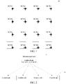
- FIG. 1 is a schematic diagram of a QMC system for multi-bit quantum feedback control according to an embodiment of the present disclosure.
- the system may include an MC network including a plurality of MCSGs 10.
- Each MCSG 10 is used as a node in the MC network and has a connection relationship with at least one another MCSG 10.
- the MC network includes a plurality of nodes, and each node corresponds to one MCSG 10.
- the nodes are connected according to a particular rule to form a two-dimensional or three-dimensional network structure.
- the MC network is a two-dimensional mesh network structure. That is, the MC network includes a plurality of nodes distributed in an array structure of M rows ⁇ N columns, both M and N being integers greater than 1. Nodes located at four vertexes of the two-dimensional mesh network are connected to two adjacent nodes. Nodes located on four edges of the two-dimensional mesh network (except the nodes at the vertexes) are connected to three adjacent nodes. Nodes located on neither vertexes nor edges of the two-dimensional mesh network are connected to four adjacent nodes. In addition, a direction of each connection coincides with a rectangular coordinate, thus forming an array structure distribution of M rows ⁇ N columns.
- Each MCSG 10 is configured to perform MC on a physical qubit group, the physical qubit group including a plurality of physical qubits.
- a quantum chip includes a plurality of physical qubits (for example, more than 50 or even more than 100), the plurality of physical qubits are divided into a plurality of physical qubit groups, and each physical qubit group includes a plurality of physical qubits.
- the numbers of physical qubits included in any two physical qubit groups may be the same or different, which is not limited in this embodiment of the present disclosure.
- the MC refers to measuring a quantum state of a physical qubit, and performing some feedback control on the physical qubit based on a measurement result. For example, by measuring the quantum state of the physical qubit, it is determined whether the quantum state of the physical qubit is erroneous, and when it is determined that the quantum state is erroneous, error correction control is performed on the quantum state of the physical qubit.
- the MCSG 10 and the physical qubit group are in a one-to-one correspondence.
- Each MCSG 10 is configured to perform MC on a physical qubit group corresponding to the MCSG 10.
- the MCSG 10 includes a measurement unit 11 and a plurality of control units 12, each control unit 12 being configured to control one physical qubit.
- the measurement unit 11 is configured to measure a quantum state of each physical qubit in the physical qubit group corresponding to the MCSG 10, and transmit a control instruction (in some paragraphs of the present disclosure, the control instruction is also referred to as a "feedback control signal") to the control unit 12 based on a measurement result.
- the control unit 12 is configured to control a corresponding physical qubit according to the control instruction.
- the MCSG 10 may include one measurement unit 11 and five control units 12.
- the measurement unit 11 is configured to measure quantum states of the five physical qubits, and generate a control instruction based on a measurement result.
- the five control units 12 and the five physical qubits are in a one-to-one correspondence, and each control unit 12 is configured to control a physical qubit corresponding to the control unit 12.
- the control unit 12 controls the corresponding physical qubit to perform a corresponding operation according to the control instruction.
- a corresponding physical circuit may be designed to implement a corresponding function.
- the function of the MCSG 10 may be implemented by designing a corresponding FPGA board.
- FPGA is a product of further development on the basis of programming devices such as programming array logic (PAL) and generic array logic (GAL).
- PAL programming array logic
- GAL generic array logic
- the FPGA emerges as a semi-custom circuit in the application-specific integrated circuit (ASIC) field, which overcomes shortcomings of a custom circuit, and shortcomings of a limited number of gate circuits of an original programming device.
- a bidirectional data transmission channel between two MCSGs 10 having a connection relationship there is a bidirectional data transmission channel between measurement units 11 of the two MCSGs 10 having a connection relationship.
- a measurement unit 11 of one MCSG 10 may transmit the measurement result to a measurement unit 11 of the other MCSG 10 through the data transmission channel, to share measurement results among the MCSGs 10.
- the data transmission channel between the MCSGs 10 can be configured to transmit other data in addition to the measurement result, which is not limited in this embodiment of the present disclosure.
- a physical connection (that is, a physical transmission channel) is established between the two MCSGs 10 (for example, the measurement units 11 of the two MCSGs 10) to implement the bidirectional data transmission channel through the physical connection.
- a physical connection that is, a physical transmission channel
- the two MCSGs 10 for example, the measurement units 11 of the two MCSGs 10.
- general input and output pins of FPGA of adjacent MCSGs 10 may be directly interconnected by simply using a cable, or a twisted pair may be used for interconnection, or a high-speed serial unit of the FPGA is used and an optical fiber/coaxial cable is used as a physical channel to further improve a data transmission rate of a single channel.
- no special requirements are imposed on the hardware implementation, and a user selects different connection solutions according to different hardware restrictions or system parameter requirements.
- connection channels provided on the board, more information may be transmitted in parallel, a bandwidth of a network is larger, and a propagation delay of data exchanged between MCSGs is smaller, which is more beneficial to achieving low-delay quantum feedback control.
- the promising SCQC mostly aggregates SC qubits in a manner of a planar grid
- the MC system uses the same structure (that is, a two-dimensional planar network structure, as the two-dimensional mesh network structure shown in FIG. 1 )
- a one-to-one correspondence between a location of an MC channel and a location of a controlled physical qubit may be implemented, to facilitate programming control.
- coupling between physical qubits that are adjacent to each other is used, and the physical qubits that are adjacent to each other are generally used for encoding logical qubits.
- a group of physical qubits share a set of hardware of an MC system, to utilize a spatial locality of a quantum operation. In this way, a transmission delay of a system feedback signal and an amount of communication between physical boards may be minimized.
- a requirement of a QEC algorithm is to quickly perform quantum state measurement on a plurality of physical qubits, generate an error correction code and a feedback control signal according to a measurement result, and distribute the error correction code and the feedback control signal to a control unit.
- a measurement unit in the MCSG may transmit less measurement results of the group to another MCSG, but directly generate error correction codes in the group and distribute feedback control signals to control units in the group, to implement quick feedback. Setting up the MCSG can effectively utilize a system bandwidth and reduce a delay.
- Each MCSG 10 is responsible for a group of physical qubits located close to each other.
- a signal transmission delay in the MCSG 10 is a very small constant. Therefore, physical qubits used in QEC can be regarded as a controlled group, and a gate operation of a logical qubit can be implemented in the group.
- MCSGs are expanded into an MC network, so that the MC network may be expanded in sequence and has characteristics of scalability and reconfigurability to meet the requirements of running a quantum feedback algorithm on a large number of (for example, more than 100) physical qubits.
- the following describes an internal interconnection manner of the MCSG 10. For example, according to a resource situation of a physical board (the following mainly uses the FPGA board as an example), it may be determined whether to use a plurality of physical boards as an MCSG 10 in a networking manner.
- a measurement unit and a control unit in the same MCSG are deployed in the same physical board.
- an MCSG 10 including one measurement unit 11 and a plurality of control units 12 may be virtualized based on the FPGA board.
- an intra-group interconnection structure may not be necessary. All data processing units of the virtual measurement unit and control units are deployed in the same FPGA board (or referred to as an FPGA chip), and nodes naturally share information in the board without transmitting the information through an inter-board transmission channel.
- the measurement unit and the control unit in the same MCSG are deployed in different physical boards, and there is a unidirectional inter-board transmission channel between the measurement unit and the control unit.
- each board can be used to virtualize only one measurement unit 11 or two control units 12, an appropriate intra-group interconnection structure may need to be designed, to distribute a control signal generated by the measurement unit 11 to a corresponding control unit 12.
- a tree-like subgroup structure can be adopted. As shown in FIG. 2 , a measurement unit 11 is a parent node, and control units 12 are child nodes.
- the parent node is connected to each child node through a unidirectional transmission channel (WR channel) (here the emphasis is on an inter-board transmission channel).
- the transmission channel is responsible for transmitting a synchronization trigger signal and a feedback control signal transmitted from the measurement unit 11 to the control unit 12.
- the transmission channel is also responsible for writing data and instructions into the control unit.
- how many physical qubits that each MCSG may need to be responsible for may be planned, and how many control units and measurement units are needed and board resources required by each unit are analyzed according to a bit control requirement.
- an MCSG may be implemented on the FPGA board. In this case, it may not be needed for more boards to combine to implement an MCSG.
- an existing FPGA boards can implement only one measurement unit or one control unit, it may be considered that more FPGA boards are required to be connected in a specific manner to form a subnet (a tree structure shown in FIG. 2 ) of an MCSG.
- the FPGA board in which the measurement unit is located is used as a main unit of the MCSG, and carries a router of a system network node.
- a group of physical qubits share a set of hardware of an MC system by setting up an MCSG.
- a measurement unit in the MCSG directly generates an error correction code in the group and distributes feedback control signals to control units in the group, to implement quick feedback, thereby reducing an amount of communication between physical boards.
- a quantum operation on an SCQC has a spatial locality, and the measurement unit in the MCSG can forward more measurement results of this group to other adjacent MCSGs with a lower delay. Setting up the MCSG may minimize a communication delay of a system network and a running time of a QEC algorithm.
- some special error correction code solutions may need to use a plurality of physical qubit groups. Therefore, implementation of an error correction code depends on cooperative work of a plurality of MCSGs in the present disclosure. To meet universality, a measurement result of an MCSG may need to be quickly transmitted to adjacent nodes through a network. In the present disclosure, because there is a bidirectional data transmission channel between two MCSGs having a connection relationship, the measurement result may be transmitted through the data transmission channel between the MCSGs, to meet the above implementation requirements.
- An MCSG is configured with corresponding node coordinates, and the node coordinates are used for identifying a location of the MCSG in an MC network.
- the node coordinates may include a horizontal coordinate (X coordinate) and a vertical coordinate (Y coordinate).
- An X coordinate and a Y coordinate of each node (MCSG) may be respectively configured through DIP switches on a physical board (for example, an FPGA board).
- each node can read its node coordinates according to a first DIP switch and a second DIP switch on the FPGA board.
- the first DIP switch is configured to set a horizontal coordinate (X coordinate) of the node
- the second DIP switch is configured to set a vertical coordinate (Y coordinate) of the node.
- a DIP switch sw_x[7:0] is configured to set the X coordinate of the node
- a DIP switch sw_y[7:0] is configured to set the Y coordinate of the node.
- [7:0] is the wording of a hardware bit width, which means that there are 8 bits, and the most significant bit is in front.
- an identifier is assigned to each measurement unit, and the identifier includes the node coordinates corresponding to the MCSG to which the measurement unit belongs.
- a media access control (MAC) address (which is not necessarily in a form of a MAC address, but may be another custom identifier of a network node) is assigned to each measurement unit, and the last byte of the address and the coordinates of the node are in a one-to-one correspondence.
- a MAC address DE:AD:BE:EF:00:31 represents a node located in a second column and a fourth row
- a MAC address DE:AD:BE:EF:00:00 represents a node located at a coordinate origin (that is, a first column and a first row).
- the user may use a computer to access a memory of a node through an Ethernet/peripheral component interconnect express (PCIe, a high-speed serial computer expansion bus) interface, to directly configure a register and debug a target node.
- PCIe Ethernet/peripheral component interconnect express
- the register herein is responsible for storing working state information that may need to be quickly obtained when a program is running, for example, an identity (ID), a delay, and a feedback threshold of a node.
- Debugging nodes means to individually test and configure a working state of each node in an early period of a system configuration process.
- the MCSG is configured with a corresponding memory space, and the measurement unit and the control unit in the same MCSG share the memory space.
- the measurement unit may transmit a write instruction to the control unit to write data of a quantum program and a control waveform into a memory of the control unit.
- each node has an independent memory space.
- all units including the measurement unit and the control unit) share such a memory.
- an independent memory addressing range is allocated to the each unit, to facilitate memory access from a user or another node.
- Table 1 0x0000_0000 ⁇ 0x001F_FFFF Measurement unit 0 0x0020_0000 ⁇ 0x002F_FFFF Control unit 1 0x0030_0000 ⁇ 0x003F_FFFF Control unit 2 0x0040_0000 ⁇ 0x004F_FFFF Control unit 3 0x0050_0000 ⁇ 0x005F_FFFF Control unit 4 0x0060_0000 ⁇ 0x006F_FFFF Control unit 5 0x0070_0000 ⁇ 0x007F_FFFF Control unit 6 0x0080_0000 ⁇ 0x008F_FFFF Control unit 7 0x0090_0000 ⁇ 0x009F
- the node coordinate configuration and node memory configuration are performed on the MC network, so that each node has its own node coordinates and memory space, which facilitates communication between nodes, and storage and access of node-related information.
- the present disclosure proposes to use the following three synchronization technologies in combination:
- the present disclosure provides a synchronization solution in which a master node is used to sequentially trigger slave nodes.
- the main idea is to set a node in the MC network as a master node for synchronization, for example, a node with coordinates (0, 0) is set as master node, and nodes at the remaining coordinates are set as the slave nodes to be triggered.
- the master node is responsible for sequentially transmitting synchronization trigger signals to the slave nodes.
- Each slave node waits for a plurality of clock cycles according to a sequence of the synchronization trigger signals received, and then starts to work. In this way, global synchronization may be implemented by configuring the number of waiting cycles for each node.
- a node at a target location in the MC network is a master node, and nodes at other locations are slave nodes.
- the number of master nodes is one, and nodes other than the master node are all slave nodes.
- a node with coordinates (0, 0) may be selected as a master node.
- a node at another location may alternatively be selected as a master node. This is not limited in this embodiment of the present disclosure.
- the master node is configured to transmit a synchronization trigger signal to each slave node.
- the slave node is configured to determine a clock cycle for starting work according to a clock cycle of the received synchronization trigger signal and a pre-configured number of waiting cycles. Clock cycles for starting work of the nodes in the MC network are the same.
- a node at a coordinate origin (0, 0) is set as a master node.
- a measurement unit of the master node sequentially transmits synchronization trigger signals to all slave nodes in the MC network according to a transmission rule (an X coordinate is prioritized over a Y coordinate) specified by a network router.
- a transmission rule an X coordinate is prioritized over a Y coordinate
- the master node first transmits the synchronization trigger signal, and according to the rule of the router, the synchronization trigger signal is sequentially transmitted to slave nodes located at (3, 0), (3, 1), (3, 2), and (3, 3).
- a channel width of the network is 4 (the channel width may be understood as the number of bits that may be transmitted in a clock cycle).
- Each synchronization trigger signal herein includes exactly 4 bits.
- a delay of a synchronization trigger signal transmitted from one node to another node is one clock cycle.
- the measurement unit and the control units are all deployed on one FGPA board, all units share a synchronization trigger signal of the node at which the units are located, and wait for the same number of clock cycles and then simultaneously start working.
- the FPGA board on which the measurement unit is located may be used as a master synchronization unit.
- the master synchronization unit distributes synchronization trigger signals to the control units through inter-board interconnection channels. After receiving the synchronization trigger signal, the control unit waits for a pre-configured number of clock cycles to compensate for a delay of inter-board interconnection communication, to finally implement synchronization of all MC units in the MCSG.
- Network node trigger synchronization ensures that the control unit and the measurement unit simultaneously generate and receive digital waveforms at a relatively rough timescale of an FPGA clock cycle. Synchronization requirements for an analog waveform are more stringent. To ensure accuracy of MC, time uncertainty of sampled signals of all waveforms may need to be less than 50 ps.
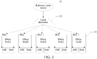
- the QMC system provided in the embodiments of the present disclosure further includes a reference clock source and a clock distributor.
- the reference clock source is configured to generate a system reference clock.
- the clock distributor is configured to distribute the system reference clock to a phase-locked loop (PLL) of each physical board.
- the PLL is configured to generate working clocks of the measurement unit and the control unit on the physical board, and generate sampling clocks of the AD conversion circuit and the DA conversion circuit on the physical board.
- a low-noise reference clock source 31 is first used, and a clock distributor 32 is then used to respectively connect reference clocks outputted by the clock source to FPGA boards 33.
- Each FPGA board has a PLL. Under configuration of a user host, the PLL locks a phase of a sampling clock generated by a board with a phase of a reference clock inputted from outside. Obviously, performance indexes of the reference clock source and the PLL determine coherence and stability of the sampling clocks of all AD/DA conversion circuits in the system, and finally determine quality of phase synchronization of a TX channel and a RX channel.
- phase differences of microwaves generated/received by all channels are stable (phase noise has been controlled within an appropriate range).
- phase noise has been controlled within an appropriate range.
- a random phase difference between the MCSGs is compensated for by using software. For example, before running a quantum program, software is used to compensate for such a random phase difference, to finally implement accurate phase synchronization.
- a microwave detection device is used to simultaneously capture pulses outputted by channels, extract delays between the channels, compensate for the delays on a computer, and transmit compensated digital waveform data to each unit, to accurately synchronize phases of a plurality of channels.
- a measurement result of a controlled physical qubit may need to be quickly obtained, and a feedback control signal may need to be generated according to the measurement result. Then the control signal is distributed to a control unit to perform feedback control. Methods for transmitting the measurement result and the feedback signal are introduced herein with reference to the network architecture of the present disclosure.
- an existing QEC theory proposes to use an error correction code to encode a logical qubit.
- a QEC code [[n,k,d]] represents to use n physical qubits to encode k logical qubits, to correct any (d-1)/2 errors that occur on any single qubit.
- n physical qubits on the SCQC are used as a controlled subgroup, and the QEC algorithm is run in the subgroup.
- Quantum feedback control in the MCSG is an important part of the QEC algorithm.
- a measurement unit transmits a synthesized dispersion pulse to the SCQC.
- the synthesized dispersion pulse is used for dispersive readout and is synthesized from pulses of different frequencies and amplitudes. Each pulse is responsible for measuring a physical qubit.
- An RX channel of the measurement unit synchronously receives a returned dispersion pulse carrying quantum state information through coupling between an SC qubit and a microwave transmission line.
- an AD conversion circuit samples and measures an echo pulse, and transmits a digitized waveform to a processor of the measurement unit.
- the processor extracts, from the waveform, a feature phase and an amplitude of a signal at a bit reading frequency, and then compares obtained feature information with a state determining threshold, to obtain a quantum state (0 or 1) of the SC qubit.
- the measurement unit Based on the measurement result of the quantum state of the SC qubit in the group, the measurement unit then runs a specific quantum feedback algorithm (for example, qubit initial state preparation, or feedback error correction based on a stabilizer code) to generate a feedback control signal and transmit the feedback control signal to the control unit, to perform a feedback operation.
- a specific quantum feedback algorithm for example, qubit initial state preparation, or feedback error correction based on a stabilizer code
- the feedback control signal is transmitted only to a control unit corresponding to an erroneous physical qubit.
- a tree-like MCSG interconnection is used as an example to illustrate a manner in which the measurement unit distributes feedback control signals.
- the measurement unit obtains a control tag of each qubit (assuming that a tag value is 0 or 1, which is used for distinguishing two different feedback operations), and distributes a control tag of the SC qubit (that is, the foregoing feedback control signal) to a corresponding control unit of the SC qubit.
- a signaling format of the feedback control signal includes a first field and a second field, the first field being used for filling a start bit of the feedback control signal, and the second field being used for filling a code bit of the feedback control signal.
- the first field is on the left, and the second field is on the right.
- a length of the first field may be 1 bit, and the first field is the start bit of the feedback control signal (for example, represented by 1), which indicates the arrival of the feedback control signal.
- a length of the second field may also be 1 bit, and the second field is the code bit of the feedback control signal.
- the control unit selects a feedback operation to be performed according to information encoded in the second field.
- a value of the second field is 0 or 1, which respectively represent two different tag values. When the number of feedback operations that may need to be supported is greater than 2, the number of code bits of the feedback control signal may be increased.
- Some special error correction code solutions need to use a plurality of physical qubit blocks. Therefore, implementation of an error correction code depends on cooperative work of a plurality of MCSGs in the present disclosure. To meet universality, a measurement result of an MCSG may need to be quickly transmitted to adjacent nodes through a network.
- a format of a network transmission data packet of a measurement result is first defined.
- the data packet is transmitted in a point-to-point manner, that is, any measurement unit in the system may transmit a data packet including a measurement result to any node through a network.
- a definition of the data packet of the measurement result is as follows.
- Each measurement unit has 8 measurement channels (that is, quantum states of 8 physical bits are simultaneously measured), so that feedback data occupies 8 bits.
- 8 bits are occupied by a coordinate part of the data packet. Therefore, a total length of the data packet is 16 bits.
- Table 5 X coordinate [1:0] of destination Y coordinate [1:0] of destination X coordinate [1:0] of source Y coordinate [1:0] of source Feedback data [7:0]
- a data packet transmitted from a first MCSG to a second MCSG includes: coordinate information of a source node (including node coordinates corresponding to the first MCSG), coordinate information of a destination node (including node coordinates corresponding to the second MCSG), and data content.
- the coordinate information of the source node includes an X coordinate (2 bits) and a Y coordinate (2 bits) of the source node.
- the coordinate information of the destination node includes an X coordinate (2 bits) and a Y coordinate (2 bits) of the destination node.
- the data content corresponds to the feedback data in Table 5, which has 8 bits.
- a data packet may need to be decomposed into four parts to be sequentially transmitted to a destination node.
- a measurement unit starts to execute a quantum feedback algorithm, and the subsequent feedback control process is described above.
- a wormhole router and a virtual channel flow control method are specifically designed for a QMC network.
- a wormhole router is integrated in a measurement unit of an MCSG, the wormhole router includes a plurality of ports, and a physical transmission channel (for example, a bidirectional data transmission channel) is formed through corresponding ports between wormhole routers of two MCSGs having a connection relationship.
- the wormhole router is configured to split a data packet into flits of a fixed length and transmit the flits.
- the router is integrated on a physical board on which a measurement unit of each network node (MCSG) is located.
- the router can control a flow direction and volume of a data packet in a network.
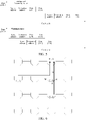
- a schematic diagram of a wormhole router 40 is shown in FIG. 4 , and the router herein has an order of 5, respectively corresponding to 5 transmission directions: east (E), west (W), south (S), north (N), and a processor (P) of the router.
- the wormhole router is used to resolve the foregoing problem.
- a function of the wormhole router is to decompose a relatively long network data packet into flits of a relatively small fixed length.
- a width of the flit is equal to the number of bits that can be simultaneously transmitted in a network (that is, a bit width of a connection channel in one direction, which may be as small as 4 bits or even 2 bits). Therefore, the wormhole router is applicable to an inter-board communication network with limited hardware resources.
- a dimension-prioritized signal transmission policy is adopted in a router design, which can prove that this method can well balance load on a network channel involving non-uniform traffic mode (for example, replacement traffic, n-to-one transmission, or one-to-n transmission), and can keep a path length as short as possible to reduce an average delay of data packets.
- Dimensionally ordered routing usually does not include transmission from a second dimension to a first dimension. For example, for routing with an X coordinate prioritized over a Y coordinate, a data packet may never be propagated from a Y direction to an X direction. Therefore, a request from (north, south) to (west, east) never exists in the router.
- a direction P may be particular in a network, which represents a node itself.
- the node itself can access any direction (including the direction P) of the router of the node, and can be accessed by any other direction.
- a System Verilog hardware description language is used to design the router, a logic circuit is generated through a digital synthesis tool, and the router is finally implemented on an FPGA.
- the router also supports multi-dimensional topological connections, and a width of a flit can also be changed according to an actual number of physical layer channels.
- a width of a physical channel is 4 bits is used herein, to analyze a propagation process of 8-bit feedback data in a 4 ⁇ 4 network.
- a transmission policy of the router is that an X coordinate is before a Y coordinate.
- a node located at (0, 0) may need to continuously transmit two feedback data packets to nodes (0, 2) and (0, 3). Then, both data packets pass through a router located at a node (0, 1), and occupy a W-to-E routing channel.
- An advantage of the wormhole router over a general buffering-transmitting router is that the wormhole router can move a flit to a next node without storing an entire data packet. Therefore, in this example, as shown in FIG. 5 , the router may need to buffer only a first flit of the data packet, that is, an X/Y coordinate of a destination node, to determine a transmission direction of a next flit.
- a total delay of the router is 2(3)+4 clock cycles.
- 2(3) is a network transmission delay of a first (second) feedback data packet, which is proportional to the number of nodes through which information passes.
- 4 is a data conversion delay, which is proportional to the number of flits of the data packet. Therefore, when many network data packets in the same direction may need to pass through the router, the network data packets are transmitted to respective destination nodes in a pipeline manner. Compared with the buffering-transmitting router, this design can better use a bandwidth of a transmission channel and reduce an average delay of a plurality of signals transmitted on a network.
- a bidirectional data transmission channel between two MCSGs having a connection relationship may include two unidirectional data transmission channels. That is, assuming that there is a connection relationship between the first MCSG and the second MCSG, there are a unidirectional data transmission channel 1 and a unidirectional data transmission channel 2 between the first MCSG and the second MCSG. In addition, a direction of the unidirectional data transmission channel 1 is from the first MCSG to the second MCSG, and a direction of the unidirectional data transmission channel 2 is from the second MCSG to the first MCSG.
- Each unidirectional data transmission channel corresponds to a plurality of virtual transmission channels.
- the data packets from different transmission paths occupy different virtual transmission channels, and data transmission is performed in sequence between the virtual transmission channels according to a set flow control policy.
- a width of each channel may be so small that a plurality of flits cannot be simultaneously transmitted.
- a port channel used by the router is occupied. In this case, requests of other data packets to the router are suspended, and the data packets are temporarily stored in a buffer at a front end of the router and wait for transmission, until a previous data packet is entirely transmitted to a next node.
- Such first-come, first-served channel flow control may cause network congestion.
- a node with coordinates (2, 2) transmits a feedback control signal to a node (0, 2)
- a node with coordinates (1, 0) also transmits a feedback control signal to the node (0, 2).
- both data packets may need to occupy an N port of a router of a node (1, 2).
- the data packet from the node (2, 2) arrives at the router (1, 2) first, and is processed first.
- the destination node (0, 2) cannot receive the data packet from the node (2, 2) temporarily, the N port and an S port of the router (1, 2) are blocked, and transmission of the data packet from the node (1, 0) is further blocked. It is conceivable that because the transmission of the second data packet cannot be performed in time, the second data packet occupies network channel resources for a long time, further resulting in deterioration of service quality of other routers, and finally, an entire network is increasingly congested.
- a manner of virtual channel flow control is adopted, so that different virtual channels share the same physical channel. That is, on an existing physical channel, a plurality of independent channels that can be used are virtualized. Network packets from different transmission paths can occupy any virtual transmission channel so that the same physical channel is multiplexed for different network packets.
- a cyclic fair flow control policy is used to control priorities of responses of the virtual channel, that is, each network packet has the same possibility to obtain a virtual channel service and pass through a router on a path of the network packet.
- Such a virtual channel flow control solution can evenly allocate bandwidth resources of the physical channel.
- Signal flows in FIG. 6 are still used as an example.
- a first flit from the node (2, 2) is transmitted from the router (1, 2) to the node (0, 2), a first flit from the node (1, 0) and a second flit from the node (2, 2) simultaneously request to pass through the N port of the router (1, 2).
- a flow control module of the router chooses to respond to a request from the S port or a W port according to the cyclic fair policy. Assuming that the first flit from the node (2, 2) passes through the router at first, the first flit from the node (1, 0) passes through the router next, and so on.
- this manner reduces a probability of network congestion and effectively increases a bandwidth of the router, thereby reducing an overall network delay.
- this method can also reduce data that may need to be buffered at the router and the node, saving memory resources of an FPGA.
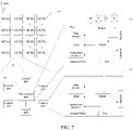
- FIG. 7 is a hierarchical diagram of system composition of a QMC system according to the present disclosure.
- the QMC system includes an MC network including a plurality of MCSGs 10.
- Each MCSG 10 includes one measurement unit 11 and a plurality of control units 12, and circuit structures of the measurement unit 11 and the control unit 12 are shown in FIG. 7 .
- the measurement unit in each MCSG is connected to a computer through a PCIe interface or an Ethernet interface, and is individually configured and debugged by a host.
- the entire system can also work in a networking mode, that is, only one node is connected to the computer, while the remaining nodes indirectly perform data exchange with the host through a mesh network of the entire system.
- a node (0, 0) is selected to be connected to the host.
- FIG. 8 specifically depicts a process of configuring the system.
- an MIMD program running manner is selected.
- an instruction set applicable to an MIMD model is defined, which may specifically include two types.
- TXI transmit instruction
- RXI receive instruction
- FIG. 9 is a schematic diagram of a program execution process of a QMC system, a part shown in a dashed box being QEC macro instructions, which implements a logical qubit under protection of a QEC code.
- a distributed network structure and a programming model of MIMD are adopted, so that a system bandwidth may be used more effectively to improve a running speed of the quantum program.
- a novel system network architecture applied in the field of superconducting QMC is provided, which greatly reduces a delay of feedback control.
- a two-dimensional mesh network interconnection mode is adopted.
- a feedback delay between MCSGs is reduced from O(N) to O(N 0.5 ).
- a delay between the MCSGs is 100, but if a two-dimensional mesh network structure is adopted, a maximum delay between the MCSGs is 2 ⁇ 10-1.
- a networking manner of the present disclosure is flexible and facilitates integration.
- a manner that software defines hardware is adopted.
- a structure of each MCSG may be customized according to an actual quantum chip structure.
- a hardware controller/accelerator may further be added to a virtual node, and finally, an entire system is implemented on an FPGA board cluster.
- a customized virtual node and an MC instruction set does not depend on a specific hardware circuit board, and it may not be needed to design a centralized control board.
- the solutions shown in the present disclosure may reduce costs.
- Each MCSG can work individually or form a work group, and the number of control boards in each MCSG can also be easily expanded.
- the solutions are applied to small-scale dedicated quantum chips and general quantum chips with 100+ integration.
- pulse sequence synchronization and measurement data exchange are performed between groups through a two-dimensional mesh network, and a control unit in each group generates feedback control based on the measurement data.
- a quantum compiler developed based on a quantum instruction set in the present disclosure can convert a quantum algorithm of a surface code into a QMC instruction, to implement quantum feedback control.
- the ISA defined in the present disclosure is a simplified instruction set system.
- This system defines a basic pulse waveform read from a main memory and a reference waveform used for demodulation, which brings a plurality of advantages.
- pulse waveform and measurement reference waveform data may need to be pre-loaded into a corresponding MC unit.
- a new gate operation may need to be loaded, and waveform data of a quantum gate used in a previous program is multiplexed, which greatly reduces data transmitted from the host to a board and improves running efficiency.
- variables can be dynamically set by the host. This feature is very useful for adaptively calibrating a multi-qubit system, for example, adjusting a feedback threshold.
- the ISA naturally supports feedback/feedforward control and multi-signal qubits and multi-target qubits.
- this ISA imitates features of a conventional computer model, for example, a memory operation, branching, and MIMD. Therefore, the ISA has the prospect of integration with a classic processor. In the future, more complex functions can be built on the ISA, for example, a compiler for a quantum feedback program, a hardware accelerator for an error correction code, and a quantum feedback running environment.
- a hardware accelerator may be added to the measurement unit to improve a measurement speed.
- a supervisory neural network accelerator 11a may be added to a measurement unit 11 to improve accuracy and a speed of analyzing a measurement signal.
- a low-noise direct current bias channel 12a may be added to a control unit 12 to facilitate adjustment of an operating point of each bit.
- a general-purpose processor may be integrated at each node, so that entire hardware supports a C language or a higher-level general programming language, to facilitate development and promotion of a quantum programming language.
- step numbers described in the present disclosure merely exemplarily show a possible execution sequence of the steps.
- the steps may not be performed according to the number sequence.
- two steps with different numbers may be performed simultaneously, or two steps with different numbers may be performed according to a sequence contrary to the sequence shown in the figure. This is not limited in the embodiments of the present disclosure.
Landscapes
- Engineering & Computer Science (AREA)
- Physics & Mathematics (AREA)
- Theoretical Computer Science (AREA)
- General Physics & Mathematics (AREA)
- Data Mining & Analysis (AREA)
- Mathematical Physics (AREA)
- Evolutionary Computation (AREA)
- Computational Mathematics (AREA)
- Mathematical Analysis (AREA)
- Mathematical Optimization (AREA)
- Pure & Applied Mathematics (AREA)
- Computing Systems (AREA)
- General Engineering & Computer Science (AREA)
- Condensed Matter Physics & Semiconductors (AREA)
- Software Systems (AREA)
- Artificial Intelligence (AREA)
- Computer Networks & Wireless Communication (AREA)
- Signal Processing (AREA)
- Data Exchanges In Wide-Area Networks (AREA)
- Superconductor Devices And Manufacturing Methods Thereof (AREA)
- Testing Or Calibration Of Command Recording Devices (AREA)
- Logic Circuits (AREA)
Applications Claiming Priority (2)
| Application Number | Priority Date | Filing Date | Title |
|---|---|---|---|
| CN202011239260.6A CN113011591B (zh) | 2020-11-09 | 2020-11-09 | 一种用于多比特量子反馈控制的量子测控系统 |
| PCT/CN2021/080602 WO2022095319A1 (zh) | 2020-11-09 | 2021-03-12 | 一种用于多比特量子反馈控制的量子测控系统 |
Publications (2)
| Publication Number | Publication Date |
|---|---|
| EP4024293A4 EP4024293A4 (de) | 2022-07-06 |
| EP4024293A1 true EP4024293A1 (de) | 2022-07-06 |
Family
ID=81453892
Family Applications (1)
| Application Number | Title | Priority Date | Filing Date |
|---|---|---|---|
| EP21759007.4A Pending EP4024293A1 (de) | 2020-11-09 | 2021-03-12 | Quantenmess- und -steuersystem für multi-bit-quantenrückkopplungssteuerung |
Country Status (4)
| Country | Link |
|---|---|
| US (1) | US12401491B2 (de) |
| EP (1) | EP4024293A1 (de) |
| JP (1) | JP7355983B2 (de) |
| KR (1) | KR20220063759A (de) |
Families Citing this family (13)
| Publication number | Priority date | Publication date | Assignee | Title |
|---|---|---|---|---|
| US11740901B2 (en) * | 2021-06-15 | 2023-08-29 | International Business Machines Corporation | Centralized control of execution of quantum program |
| EP4174733A1 (de) * | 2021-10-26 | 2023-05-03 | Electronics and Telecommunications Research Institute | Quantenrechensystem und verfahren zum betreiben desselben |
| US12602245B2 (en) * | 2021-11-18 | 2026-04-14 | Red Hat, LLC | Quantum isolation zoneslc |
| US12524691B2 (en) * | 2022-04-26 | 2026-01-13 | International Business Machines Corporation | Central controller for a quantum system |
| US12541703B2 (en) | 2022-04-26 | 2026-02-03 | International Business Machines Corporation | Multitasking scheme for quantum computers |
| CN117273159B (zh) * | 2022-06-14 | 2025-09-19 | 本源量子计算科技(合肥)股份有限公司 | 量子态驱动信号发生器、装置、以及量子计算机系统 |
| CN117669747A (zh) * | 2022-09-01 | 2024-03-08 | 腾讯科技(深圳)有限公司 | 量子比特测控系统的波形传输方法、系统及存储介质 |
| CN115688928B (zh) * | 2022-09-20 | 2025-02-11 | 中国科学院自动化研究所 | 反馈控制方法、系统、装置及设备 |
| US12273269B1 (en) * | 2022-11-08 | 2025-04-08 | Marvell Asia Pte Ltd | Selective mesh routing through non-adjacent nodes |
| US12353764B1 (en) | 2022-11-10 | 2025-07-08 | Marvell Asia Pte Ltd | Single cycle request arbiter |
| CN116862008B (zh) * | 2023-07-31 | 2025-07-29 | 国仪量子技术(合肥)股份有限公司 | 离子态信息采集方法与装置、存储介质、测控系统 |
| GB2643110A (en) * | 2024-07-30 | 2026-02-11 | Riverlane Ltd | A method of performing qubit operations |
| CN120929140A (zh) * | 2025-07-29 | 2025-11-11 | 杭州标彰电子科技有限公司 | 一种基于多线程并行路由的量子设备指令分发系统及方法 |
Family Cites Families (9)
| Publication number | Priority date | Publication date | Assignee | Title |
|---|---|---|---|---|
| JP2000101597A (ja) * | 1998-09-24 | 2000-04-07 | Nec Corp | ノード間フレーム位相同期方式及び方法 |
| US8861664B2 (en) * | 2012-06-15 | 2014-10-14 | Smsc Holdings S.A.R.L. | Communication system and method for synchronizing a plurality of network nodes after a network lock condition occurs |
| CN104158515B (zh) * | 2014-07-29 | 2016-08-10 | 电子科技大学 | 一种自动同步的多通道并行存储dds信号发生器 |
| CN104901905B (zh) | 2015-04-27 | 2018-07-03 | 国家电网公司 | 一种智能变电站专用网络交换机及其数据交换方法 |
| US10776709B2 (en) | 2016-11-10 | 2020-09-15 | Yale University | Generalized quantum channels |
| US11694104B2 (en) | 2017-08-09 | 2023-07-04 | Google Llc | Reducing parasitic interactions in a qubit grid |
| US11238360B2 (en) | 2018-02-12 | 2022-02-01 | International Business Machines Corporation | Fast quantum feedback using analog integration and control pulse gating |
| CN109217939B (zh) * | 2018-06-20 | 2020-12-18 | 浙江大学 | 用于量子比特的可扩展、低延迟反馈调控设备 |
| CN109800882B (zh) | 2018-12-28 | 2020-10-09 | 华东计算技术研究所(中国电子科技集团公司第三十二研究所) | 多位超导量子比特的扩展反馈测量装置 |
-
2021
- 2021-03-12 EP EP21759007.4A patent/EP4024293A1/de active Pending
- 2021-03-12 KR KR1020217032064A patent/KR20220063759A/ko active Pending
- 2021-03-12 JP JP2021547817A patent/JP7355983B2/ja active Active
- 2021-10-11 US US17/498,671 patent/US12401491B2/en active Active
Also Published As
| Publication number | Publication date |
|---|---|
| EP4024293A4 (de) | 2022-07-06 |
| JP2023508791A (ja) | 2023-03-06 |
| JP7355983B2 (ja) | 2023-10-04 |
| US20220150044A1 (en) | 2022-05-12 |
| US12401491B2 (en) | 2025-08-26 |
| KR20220063759A (ko) | 2022-05-17 |
Similar Documents
| Publication | Publication Date | Title |
|---|---|---|
| US12401491B2 (en) | Quantum measurement and control system for multi-bit quantum feedback control | |
| CN113011591B (zh) | 一种用于多比特量子反馈控制的量子测控系统 | |
| Ajima et al. | The tofu interconnect d | |
| US12335099B2 (en) | Enhanced reconfigurable interconnect network | |
| Biswas et al. | Accelerating tensorflow with adaptive rdma-based grpc | |
| Katevenis et al. | Next generation of Exascale-class systems: ExaNeSt project and the status of its interconnect and storage development | |
| Wang et al. | Step-3 is large yet affordable: Model-system co-design for cost-effective decoding | |
| Sun et al. | Multi-node acceleration for large-scale GCNs | |
| Ueno et al. | VCSN: Virtual circuit-switching network for flexible and simple-to-operate communication in HPC FPGA cluster | |
| Hamidouche et al. | GPU-Initiated Networking for NCCL | |
| Pham et al. | Scalable low-latency inter-FPGA networks | |
| Chidella et al. | Impact of non-uniform subnets on the performance of wireless network-on-chip architectures | |
| Tang et al. | MoEntwine: Unleashing the Potential of Wafer-scale Chips for Large-scale Expert Parallel Inference | |
| CN116910969A (zh) | 一种万节点级电磁暂态实时仿真平台及电磁暂态仿真方法 | |
| Liu et al. | High‐speed end‐to‐edge data caching and forwarding architecture based on field programmable gate array | |
| Huang et al. | Improving the efficiency of HPC data movement on container-based virtual cluster | |
| US20140269765A1 (en) | Broadcast Network | |
| Zhang et al. | A homogeneous many-core x86 processor full system framework based on NoC | |
| Vemuri et al. | Communication-Centric UALink and NVLink Comparison for Large Scale AI Training | |
| Vetter et al. | HPC interconnection networks: The key to exascale computing | |
| Mnejja et al. | Exploring hybrid noc architecture for chip multiprocessor | |
| Kumar et al. | Hierarchical communication optimization for fft | |
| Dorai et al. | A novel architecture for inter-fpga traffic collision management | |
| Ijaz et al. | Wireless versus wired network-on-chip to enable the multi-tenant multi-fpgas in cloud | |
| Scales et al. | Experience with parallel computing on the AN2 network |
Legal Events
| Date | Code | Title | Description |
|---|---|---|---|
| STAA | Information on the status of an ep patent application or granted ep patent |
Free format text: STATUS: UNKNOWN |
|
| STAA | Information on the status of an ep patent application or granted ep patent |
Free format text: STATUS: THE INTERNATIONAL PUBLICATION HAS BEEN MADE |
|
| PUAI | Public reference made under article 153(3) epc to a published international application that has entered the european phase |
Free format text: ORIGINAL CODE: 0009012 |
|
| STAA | Information on the status of an ep patent application or granted ep patent |
Free format text: STATUS: REQUEST FOR EXAMINATION WAS MADE |
|
| 17P | Request for examination filed |
Effective date: 20210902 |
|
| A4 | Supplementary search report drawn up and despatched |
Effective date: 20220527 |
|
| AK | Designated contracting states |
Kind code of ref document: A1 Designated state(s): AL AT BE BG CH CY CZ DE DK EE ES FI FR GB GR HR HU IE IS IT LI LT LU LV MC MK MT NL NO PL PT RO RS SE SI SK SM TR |
|
| DAV | Request for validation of the european patent (deleted) | ||
| DAX | Request for extension of the european patent (deleted) | ||
| STAA | Information on the status of an ep patent application or granted ep patent |
Free format text: STATUS: EXAMINATION IS IN PROGRESS |
|
| 17Q | First examination report despatched |
Effective date: 20251030 |