EP4024704A1 - Leistungsverstärkerschaltung, sender und netzwerkvorrichtung - Google Patents
Leistungsverstärkerschaltung, sender und netzwerkvorrichtung Download PDFInfo
- Publication number
- EP4024704A1 EP4024704A1 EP19945716.9A EP19945716A EP4024704A1 EP 4024704 A1 EP4024704 A1 EP 4024704A1 EP 19945716 A EP19945716 A EP 19945716A EP 4024704 A1 EP4024704 A1 EP 4024704A1
- Authority
- EP
- European Patent Office
- Prior art keywords
- power amplifier
- circuit
- branch
- branches
- power
- Prior art date
- Legal status (The legal status is an assumption and is not a legal conclusion. Google has not performed a legal analysis and makes no representation as to the accuracy of the status listed.)
- Pending
Links
Images



Classifications
-
- H—ELECTRICITY
- H03—ELECTRONIC CIRCUITRY
- H03F—AMPLIFIERS
- H03F1/00—Details of amplifiers with only discharge tubes, only semiconductor devices or only unspecified devices as amplifying elements
- H03F1/02—Modifications of amplifiers to raise the efficiency, e.g. gliding Class A stages, use of an auxiliary oscillation
- H03F1/0205—Modifications of amplifiers to raise the efficiency, e.g. gliding Class A stages, use of an auxiliary oscillation in transistor amplifiers
- H03F1/0288—Modifications of amplifiers to raise the efficiency, e.g. gliding Class A stages, use of an auxiliary oscillation in transistor amplifiers using a main and one or several auxiliary peaking amplifiers whereby the load is connected to the main amplifier using an impedance inverter, e.g. Doherty amplifiers
-
- H—ELECTRICITY
- H03—ELECTRONIC CIRCUITRY
- H03F—AMPLIFIERS
- H03F1/00—Details of amplifiers with only discharge tubes, only semiconductor devices or only unspecified devices as amplifying elements
- H03F1/42—Modifications of amplifiers to extend the bandwidth
-
- H—ELECTRICITY
- H03—ELECTRONIC CIRCUITRY
- H03F—AMPLIFIERS
- H03F1/00—Details of amplifiers with only discharge tubes, only semiconductor devices or only unspecified devices as amplifying elements
- H03F1/56—Modifications of input or output impedances, not otherwise provided for
-
- H—ELECTRICITY
- H03—ELECTRONIC CIRCUITRY
- H03F—AMPLIFIERS
- H03F3/00—Amplifiers with only discharge tubes or only semiconductor devices as amplifying elements
- H03F3/189—High-frequency amplifiers, e.g. radio frequency amplifiers
- H03F3/19—High-frequency amplifiers, e.g. radio frequency amplifiers with semiconductor devices only
- H03F3/195—High-frequency amplifiers, e.g. radio frequency amplifiers with semiconductor devices only in integrated circuits
-
- H—ELECTRICITY
- H03—ELECTRONIC CIRCUITRY
- H03F—AMPLIFIERS
- H03F3/00—Amplifiers with only discharge tubes or only semiconductor devices as amplifying elements
- H03F3/20—Power amplifiers, e.g. Class B amplifiers, Class C amplifiers
- H03F3/21—Power amplifiers, e.g. Class B amplifiers, Class C amplifiers with semiconductor devices only
- H03F3/211—Power amplifiers, e.g. Class B amplifiers, Class C amplifiers with semiconductor devices only using a combination of several amplifiers
-
- H—ELECTRICITY
- H03—ELECTRONIC CIRCUITRY
- H03F—AMPLIFIERS
- H03F3/00—Amplifiers with only discharge tubes or only semiconductor devices as amplifying elements
- H03F3/20—Power amplifiers, e.g. Class B amplifiers, Class C amplifiers
- H03F3/24—Power amplifiers, e.g. Class B amplifiers, Class C amplifiers of transmitter output stages
- H03F3/245—Power amplifiers, e.g. Class B amplifiers, Class C amplifiers of transmitter output stages with semiconductor devices only
-
- H—ELECTRICITY
- H03—ELECTRONIC CIRCUITRY
- H03F—AMPLIFIERS
- H03F3/00—Amplifiers with only discharge tubes or only semiconductor devices as amplifying elements
- H03F3/60—Amplifiers in which coupling networks have distributed constants, e.g. with waveguide resonators
- H03F3/602—Combinations of several amplifiers
-
- H—ELECTRICITY
- H03—ELECTRONIC CIRCUITRY
- H03F—AMPLIFIERS
- H03F2200/00—Indexing scheme relating to amplifiers
- H03F2200/198—A hybrid coupler being used as coupling circuit between stages of an amplifier circuit
-
- H—ELECTRICITY
- H03—ELECTRONIC CIRCUITRY
- H03F—AMPLIFIERS
- H03F2200/00—Indexing scheme relating to amplifiers
- H03F2200/204—A hybrid coupler being used at the output of an amplifier circuit
-
- H—ELECTRICITY
- H03—ELECTRONIC CIRCUITRY
- H03F—AMPLIFIERS
- H03F2200/00—Indexing scheme relating to amplifiers
- H03F2200/222—A circuit being added at the input of an amplifier to adapt the input impedance of the amplifier
-
- H—ELECTRICITY
- H03—ELECTRONIC CIRCUITRY
- H03F—AMPLIFIERS
- H03F2200/00—Indexing scheme relating to amplifiers
- H03F2200/387—A circuit being added at the output of an amplifier to adapt the output impedance of the amplifier
-
- H—ELECTRICITY
- H03—ELECTRONIC CIRCUITRY
- H03F—AMPLIFIERS
- H03F2200/00—Indexing scheme relating to amplifiers
- H03F2200/451—Indexing scheme relating to amplifiers the amplifier being a radio frequency amplifier
-
- Y—GENERAL TAGGING OF NEW TECHNOLOGICAL DEVELOPMENTS; GENERAL TAGGING OF CROSS-SECTIONAL TECHNOLOGIES SPANNING OVER SEVERAL SECTIONS OF THE IPC; TECHNICAL SUBJECTS COVERED BY FORMER USPC CROSS-REFERENCE ART COLLECTIONS [XRACs] AND DIGESTS
- Y02—TECHNOLOGIES OR APPLICATIONS FOR MITIGATION OR ADAPTATION AGAINST CLIMATE CHANGE
- Y02D—CLIMATE CHANGE MITIGATION TECHNOLOGIES IN INFORMATION AND COMMUNICATION TECHNOLOGIES [ICT], I.E. INFORMATION AND COMMUNICATION TECHNOLOGIES AIMING AT THE REDUCTION OF THEIR OWN ENERGY USE
- Y02D30/00—Reducing energy consumption in communication networks
- Y02D30/70—Reducing energy consumption in communication networks in wireless communication networks
Definitions
- This application relates to the communications field, and in particular, to a power amplifier circuit, a transmitter, and a network device in the communications field.
- a wireless communications system has increasingly high requirements on a channel capacity and a data transmission rate.
- Present and future wireless communications systems require a power amplifier to have wideband and multi-band features, so that the power amplifier covers a plurality of frequency bands in a same communications standard and needs to be compatible with different communications standards.
- the power amplifier operates at different operating frequency bands and needs an increasingly wide signal bandwidth.
- a power amplifier is a main energy consumption module of a transceiver.
- the energy consumption of the power amplifier accounts for a high proportion of that of a wireless communications system.
- An improvement of efficiency of the power amplifier for reducing the energy consumption directly affects heat dissipation of the system, and also affects a loading capacity of a power supply. Therefore, it is a key technology for the wireless communications system to extend an operating bandwidth of the power amplifier and improve work efficiency of the power amplifier.
- Two-way Doherty (DHT), based on an active load modulation mechanism, has been widely applied to mobile base stations, for it can effectively improve back-off efficiency of a power amplifier circuit.
- Three-way, four-way, or N-way DHT may further extend a power back-off or generate a plurality of high efficiency points, to further improve power amplification efficiency.
- an operating bandwidth of the N-way DHT is usually limited due to a relatively large load pull ratio of a power transistor, and the N-way DHT cannot be used in a high-power ultra-wideband power amplifier circuit.
- This application provides a power amplifier circuit, a transmitter, and a network device, and the power amplifier circuit has features of a wide band and high efficiency.
- an embodiment of this application provides a power amplifier circuit.
- the power amplifier circuit includes N input ports, N power amplifier branches, one combiner circuit, and one output port.
- Each of the N input ports is connected to one power amplifier branch in the N power amplifier branches, each of the power amplifier branches is connected to the combiner circuit, the combiner circuit is further connected to the output port, and each input port is configured to input one input signal.
- the N power amplifier branches and the combiner circuit are configured to perform power amplification and combining on N input signals, to generate an output signal.
- the output port is configured to output the output signal.
- the N power amplifier branches include one first power amplifier branch and N-1 second power amplifier branches.
- the first power amplifier branch operates in a class AB or class B operating mode
- the N-1 second power amplifier branches operate in a class C operating mode with different gate bias voltages
- the gate bias voltages of the N-1 second power amplifier branches become lower in order
- N is a positive integer greater than 2.
- the first power amplifier branch operates in the class AB or class B operating mode
- the N-1 second power amplifier branches operate in the class C operating mode with different gate bias voltages
- the N power amplifier branches are turned on in order and are saturated in order. Therefore, a plurality of high efficiency points can be generated with different power back-offs, and back-off efficiency is improved.
- a load pull ratio is 1. Therefore, an operating bandwidth of the power amplifier circuit of this application can be guaranteed, thereby making the power amplifier circuit feature a wide band and high efficiency.
- each of the second power amplifier branches includes one first port and two second ports.
- the first port is connected to one input port, and the two second ports are separately connected to the combiner circuit.
- Each of the second power amplifier branches is configured to perform power allocation and power amplification on one of the input signals, to generate two second signals, and each of the two second signals is output to the combiner circuit through one of the second ports. Amplitudes of the two second signals are the same, and a phase difference is 90 degrees.
- the second power amplifier branches can implement a characteristic of balanced power amplification.
- each of the second power amplifier branches includes one power allocation circuit and two power amplifier sub-branches.
- a through port and a coupling port of the power allocation circuit each are connected to one of the power amplifier sub-branches.
- the two power amplifier sub-branches operate in a class C operating mode with a same bias.
- a load pull ratio is 1. This can guarantee a bandwidth of the power amplifier circuit of this application and avoid a bandwidth limit.
- the combiner circuit includes N-1 couplers and N-1 impedance matching circuits.
- One impedance matching circuit is disposed between two adjacent couplers in the N-1 couplers, and one impedance matching circuit is disposed between the output port of the power amplifier circuit and one coupler.
- An isolated port of a first coupler in the N-1 couplers is connected to an output port of the first power amplifier branch, and two balance ports of each of the N-1 couplers each are connected to one of the second power amplifier branches.
- the impedance matching circuit between the two adjacent couplers is configured to convert a characteristic impedance of a former coupler in the two adjacent couplers to a characteristic impedance of a latter coupler in the two adjacent couplers.
- a characteristic impedance of each of the N-1 couplers is determined based on optimal impedances of power transistors of the first power amplifier branch and the second power amplifier branches that operate in the class B operating mode.
- a characteristic impedance of a coupler in the combiner circuit can be determined based on an optimal impedance of a power transistor of a power amplifier branch, which can improve performance of the power amplifier circuit of this application.
- the impedance matching circuit includes at least one of a low-pass filter circuit, a high-pass filter circuit, a resonant circuit, or a microstrip line.
- the first power amplifier branch includes a power amplifier.
- the first power amplifier branch includes a Doherty circuit, an input port of the Doherty circuit is connected to an input port of the power amplifier circuit, and an output port of the Doherty circuit is connected to the combiner circuit.
- the first power amplifier branch reaches a state of voltage saturation and current saturation before the second power amplifier branches reach a state of voltage saturation and current saturation.
- an embodiment of this application provides a transmitter, including the power amplifier circuit according to any implementation of the first aspect.
- an embodiment of this application provides a network device.
- the network device includes a transceiver, a processor, and a memory, and the transceiver includes the power amplifier circuit according to any one of the first aspect.
- the power amplifier circuit includes N input ports, N power amplifier branches, one combiner circuit, and one output port.
- Each of the N input ports is connected to one power amplifier branch in the N power amplifier branches, each of the power amplifier branches is connected to the combiner circuit, and the combiner circuit is further connected to the output port; each of the input ports is configured to input one input signal; the N power amplifier branches and the combiner circuit are configured to perform power amplification and combining on N input signals, to generate an output signal; and the output port is configured to output the output signal.
- the N power amplifier branches include one first power amplifier branch and N-1 second power amplifier branches, the first power amplifier branch operates in a class AB or class B operating mode, the N-1 second power amplifier branches operate in a class C operating mode with different gate bias voltages, the gate bias voltages of the N-1 second power amplifier branches become lower in order, and N is a positive integer greater than 2. Because the N power amplifier branches are turned on in order, and are saturated in order, a plurality of high efficiency points can be generated with different power back-offs, and back-off efficiency is improved. In addition, because there is no load pull between the N power amplifier branches, a load pull ratio is 1. Therefore, an operating bandwidth of the power amplifier circuit of this application can be guaranteed, and the power amplifier circuit has features of a wide band and high efficiency.
- first”, “second”, and the like in this application are for descriptive purposes only and should not be construed as indicating or implying relative importance or be construed as indicating or implying a sequence.
- the terms “include”, “have”, and any other variant thereof are intended to cover a non-exclusive inclusion, for example, including a series of steps or units. Methods, systems, products, or devices are not necessarily limited to those explicitly listed steps or units, but may include other steps or units that are not explicitly listed or that are inherent to such processes, methods, products, or devices.
- the word such as “example” or “for example” is used to represent giving an example, an illustration, or a description.
- At least one (piece) means one or more, and "a plurality of' means two or more.
- the term “and/or” is used to describe an association relationship between associated objects, and indicates that three relationships may exist.
- a and/or B may indicate the following three cases: Only A exists, only B exists, and both A and B exist, where A and B may be singular or plural.
- the character “/” usually indicates an "or” relationship between the associated objects.
- At least one (piece) of the following or a similar expression thereof indicates any combination of the following, including any combination of one or more of the following.
- At least one (piece) of a, b, or c may represent: a, b, c, "a and b", “a and c", “b and c", or "a, b, and c", where a, b, and c may be singular or plural.
- An embodiment of this application provides a power amplifier circuit.
- the power amplifier circuit has features of a wide band and high efficiency, can generate a plurality of high efficiency points with different power back-offs to improve back-off efficiency, and can guarantee that a load pull ratio of each power transistor is 1.
- a specific structure of the power amplifier circuit refer to the following descriptions in this embodiment.
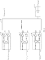
- FIG. 1 is a schematic diagram of a structure of a power amplifier circuit according to an embodiment of this application.
- the power amplifier circuit may include N input ports, N power amplifier branches, one combiner circuit 20, and one output port 30.
- the N input ports are input_1, input_2, input_3, ..., and input_N.
- the N power amplifier branches are a power amplifier branch 11, a power amplifier branch 12, ..., and a power amplifier branch IN.
- Each of the N input ports is connected to one power amplifier branch in the N power amplifier branches, each of the power amplifier branches is connected to the combiner circuit 20, and the combiner circuit 20 is further connected to the output port.
- input_1 is connected to the power amplifier branch 11
- input_2 is connected to the power amplifier branch 12
- input_3 is connected to a power amplifier branch 13
- input N is connected to the power amplifier branch IN.
- An output port of each power amplifier circuit is connected to an input port of the combiner circuit 20, and an output port of the combiner circuit is connected to the output port 30.
- Each input port (input_1, input_2, input_3, ..., and input N) is configured to input one input signal.
- the N power amplifier branches and the combiner circuit 20 are configured to perform power amplification and combining on N input signals, to generate an output signal.
- the output port 30 is configured to output the output signal.
- the N power amplifier branches include one first power amplifier branch and N-1 second power amplifier branches, where the first power amplifier branch operates in a class AB (AB) or class B (B) operating mode, the N-1 second power amplifier branches operate in a class C (C) operating mode with different gate bias voltages, the gate bias voltages of the N-1 second power amplifier branches become lower in order, and N is a positive integer greater than 2. That is, as shown in FIG. 1 , the power amplifier branch 11 is the first power amplifier branch, and the power amplifier branch 12, the power amplifier branch 13, ..., and the power amplifier branch IN are the N-1 second power amplifier branches, where gate bias voltages of the power amplifier branch 12, the power amplifier branch 13, ..., and the power amplifier branch IN become lower in order.
- the first power amplifier branch (the power amplifier branch 11) includes one input port and one output port, where the input port of the power amplifier branch 11 is connected to input_1, and the output port of the power amplifier branch 11 is connected to the input port of the combiner circuit 20.
- each of the second power amplifier branches includes one first port and two second ports, where the first port is connected to one input port, and the two second ports are separately connected to the combiner circuit 20.
- Each of the second power amplifier branches (the power amplifier branch 12, the power amplifier branch 13, ..., and the power amplifier branch IN) is configured to perform power allocation and power amplification on one input signal, to generate two second signals, and each of the two second signals is output to the combiner circuit 20 through one of the second ports. Amplitudes of the two second signals are the same, and a phase difference is 90 degrees.
- the power amplifier branch 12 includes one first port 121 and two second ports (122 and 123), where the first port 121 is connected to input_2, and the second port 122 and the second port 123 are separately connected to the combiner circuit 20.
- the power amplifier branch 12 is configured to perform power allocation and power amplification on an input signal input through input_2, to generate two second signals, and the two second signals are output to the combiner circuit 20 through the second port 122 and the second port 123.
- the power amplifier branch 13 includes one first port 131 and two second ports (132 and 133), where the first port 131 is connected to input_3, and the second port 132 and the second port 133 are separately connected to the combiner circuit 20.
- the power amplifier branch 13 is configured to perform power allocation and power amplification on an input signal input through input_3, to generate two second signals, and the two second signals are output to the combiner circuit 20 through the second port 132 and the second port 133.
- the power amplifier branch IN includes one first port 1N1 and two second ports (1N2 and 1N3), where the first port 1N1 is connected to input_N, and the second port 1N2 and the second port 1N3 are separately connected to the combiner circuit 20.
- the power amplifier branch IN is configured to perform power allocation and power amplification on an input signal input through input N, to generate two second signals, and the two second signals are output to the combiner circuit 20 through the second port 1N2 and the second port 1N3.
- a connection manner of another second power amplifier branch is the same as that of the power amplifier branch 12, the power amplifier branch 13, or the power amplifier branch IN. Illustrations are not provided herein.
- the combiner circuit 20 is configured to perform power combining of output signals from the output port of the power amplifier branch 11, the second port 122, the second port 123, the second port 132, the second port 133, ..., the second port 1N2, and the second port 1N3, and perform outputting through the output port 30.
- the power amplifier branch 11 operates in the class AB (AB) or class B (B) operating mode
- the power amplifier branch 12, the power amplifier branch 13, ..., and the power amplifier branch IN operate in the class C operating mode
- a gate bias voltage of each of the second power amplifier branches becomes lower in order, and therefore, the power amplifier branch 11, the power amplifier branch 12, the power amplifier branch 13, ..., and the power amplifier branch IN are turned on in order, and are saturated in order.
- the power amplifier branch 11 operates, and the power amplifier branch 12, the power amplifier branch 13, ..., and the power amplifier branch IN are all off.
- the power amplifier branch 12 After the power amplifier branch 11 is saturated, the power amplifier branch 12 is turned on, and the power amplifier branch 13, ..., and the power amplifier branch IN are still off, and the power amplifier branch 11 remains saturated. After the power amplifier branch 12 is saturated, the power amplifier branch 13 is turned on, and a power amplifier branch 14, ..., and the power amplifier branch IN are still off, and the power amplifier branch 11 and the power amplifier branch 12 remain saturated. This process goes on by analogy until various power amplifier branches (the power amplifier branch 14, ..., and the power amplifier branch IN) are all saturated. According to the foregoing operating principle, high efficiency points are generated at different back-off points. For example, a total of N high efficiency points are generated, thereby improving power back-off efficiency and efficiency of a modulated signal.
- the first power amplifier branch includes a power amplifier, where the power amplifier may be used as a main amplifier.
- the first power amplifier branch includes a Doherty circuit, an input port of the Doherty circuit is connected to an input port (input_1) of the power amplifier circuit, and an output port of the Doherty circuit is connected to the combiner circuit 20.
- the first power amplifier branch reaches a state of voltage saturation and current saturation before the second power amplifier branches reach a state of voltage saturation and current saturation.
- the power amplifier circuit of this embodiment includes N input ports, N power amplifier branches, one combiner circuit, and one output port, where each of the N input ports is connected to one power amplifier branch in the N power amplifier branches, each of the power amplifier branches is connected to the combiner circuit, and the combiner circuit is further connected to the output port; each of the input ports is configured to input one input signal; the N power amplifier branches and the combiner circuit are configured to perform power amplification and combining on N input signals, to generate an output signal; and the output port is configured to output the output signal, where the N power amplifier branches include one first power amplifier branch and N-1 second power amplifier branches, the first power amplifier branch operates in a class AB or class B operating mode, the N-1 second power amplifier branches operate in a class C operating mode with different gate bias voltages, the gate bias voltages of the N-1 second power amplifier branches become lower in order, and N is a positive integer greater than 2.
- the N power amplifier branches are turned on in order, and are saturated in order, a plurality of high efficiency points can be generated with different power back-offs, and back-off efficiency is improved.
- a load pull ratio is 1, and therefore, an operating bandwidth of the power amplifier circuit of this application can be guaranteed, and the power amplifier circuit has features of a wide band and high efficiency.
- M input ports of the power amplifier circuit in this embodiment of this application may be connected to an output port of one power allocation circuit.
- M of the N input signals (M is less than or equal to N) in this embodiment of this application may be M output signals from the power allocation circuit.
- one channel signal may be input into one input port of the power amplifier circuit in this embodiment of this application, and the other channel signal may be input into the power allocation circuit, where the power allocation circuit splits the channel signal into two sub-channel signals, and the two sub-channel signals may be input into other two input ports of the power amplifier circuit in this embodiment of this application.
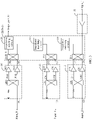
- FIG. 2 is a schematic diagram of a structure of another power amplifier circuit according to an embodiment of this application.
- each of the second power amplifier branches may include one power allocation circuit and two power amplifier sub-branches.
- a through port and a coupling port of the power allocation circuit each are connected to one of the power amplifier sub-branches, where the two power amplifier sub-branches operate in the class C (C) operating mode with a same bias.
- Each power allocation circuit is configured to perform power allocation on an input signal of an input port (input_2, input_3, ..., or input N).
- each power allocation circuit may be a coupler such as a 50-ohm coupler.
- Each of the power amplifier sub-branches is configured to perform power amplification, and may be a power amplifier.
- the power amplifier branch 12 may include a power allocation circuit 124, a power amplifier sub-branch 125, and a power amplifier sub-branch 126, where an input port of the power allocation circuit 124 is connected to input_2, and an isolated port of the power allocation circuit 124 is connected to a load.
- a through port 1241 of the power allocation circuit 124 is connected to an input port of the power amplifier sub-branch 125, and a coupling port 1242 of the power allocation circuit 124 is connected to an input port of the power amplifier sub-branch 126.
- An output port of the power amplifier sub-branch 125 is connected to the second port 122, and an output port of the power amplifier sub-branch 126 is connected to the second port 123.
- the power amplifier sub-branch 125 and the power amplifier sub-branch 126 may be two power amplifiers operating in the class C (C) operating mode with a same gate bias voltage, and the power amplifiers may be peaking amplifiers 1.
- An input signal input into input_2 is split into two signals through the power allocation circuit 124, where one of the two signals is output to the power amplifier sub-branch 125 through the through port 1241, and the other signal is output to the power amplifier sub-branch 126 through the coupling port 1242.
- a phase difference between the two signals is 90 degrees.
- the two signals are output from the power amplifier sub-branch 125 and the power amplifier sub-branch 126 to be two second signals, where amplitudes of the two second signals are the same, and a phase difference is 90 degrees.
- the power amplifier branch 13 may include a power allocation circuit 134, a power amplifier sub-branch 135, and a power amplifier sub-branch 136, where an input port of the power allocation circuit 134 is connected to input_3, and an isolated port of the power allocation circuit 134 is connected to a load.
- a through port 1341 of the power allocation circuit 134 is connected to an input port of the power amplifier sub-branch 135, and a coupling port 1342 of the power allocation circuit 134 is connected to an input port of the power amplifier sub-branch 136.
- An output port of the power amplifier sub-branch 135 is connected to the second port 132, and an output port of the power amplifier sub-branch 136 is connected to the second port 133.
- the power amplifier sub-branch 135 and the power amplifier sub-branch 136 may be two power amplifiers operating in the class C (C) operating mode with a same gate bias voltage, and the power amplifiers may be peaking amplifiers 2.
- An input signal input into input_3 is split into two signals through the power allocation circuit 134, where one of the two signals is output to the power amplifier sub-branch 135 through the through port 1341, and the other signal is output to the power amplifier sub-branch 136 through the coupling port 1342.
- a phase difference between the two signals is 90 degrees.
- the two signals are output from the power amplifier sub-branch 135 and the power amplifier sub-branch 136 to be two second signals, where amplitudes of the two second signals are the same, and a phase difference is 90 degrees.
- the power amplifier branch IN may include a power allocation circuit 1N4, a power amplifier sub-branch 1N5, and a power amplifier sub-branch 1N6, where an input port of the power allocation circuit 1N4 is connected to input_N, and an isolated port of the power allocation circuit 1N4 is connected to a load.
- a through port 1N41 of the power allocation circuit 1N4 is connected to an input port of the power amplifier sub-branch 1N5, and a coupling port 1N42 of the power allocation circuit 1N4 is connected to an input port of the power amplifier sub-branch 1N6.
- An output port of the power amplifier sub-branch 1N5 is connected to the second port 1N2, and an output port of the power amplifier sub-branch 1N6 is connected to the second port 1N3.
- the power amplifier sub-branch 1N5 and the power amplifier sub-branch 1N6 may be two power amplifiers operating in the class C (C) operating mode with a same gate bias voltage, and the power amplifiers may be peaking amplifiers (N-
- An input signal input into input N is split into two signals through the power allocation circuit 1N4, where one of the two signals is output to the power amplifier sub-branch 1N5 through the through port 1N41, and the other signal is output to the power amplifier sub-branch 1N6 through the coupling port 1N42.
- a phase difference between the two signals is 90 degrees.
- the two signals are output from the power amplifier sub-branch 1N5 and the power amplifier sub-branch 1N6 to be two second signals, where amplitudes of the two second signals are the same, and a phase difference is 90 degrees.
- Another second power amplifier branch uses a similar connection manner. Illustrations are not provided herein.
- the combiner circuit 20 is configured to perform power combining on a signal output from the first power amplifier branch and two second signals output from any second power amplifier branch in the N-1 second power amplifier branches.
- a load pull ratio is 1, which can guarantee a bandwidth of the power amplifier circuit of this application and avoid a bandwidth limit.
- FIG. 3 is a schematic diagram of a structure of another power amplifier circuit according to an embodiment of this application.
- the combiner circuit 20 may include N-1 couplers (211, 212, ..., and 21(N-1)) and N-1 impedance matching circuits (221, 222, ..., and 22(N-1)).
- One impedance matching circuit is disposed between two adjacent couplers in the N-1 couplers, and one impedance matching circuit is disposed between the output port of the power amplifier circuit and one coupler.
- An isolated port of a first coupler in the N-1 couplers is connected to an output port of the first power amplifier branch, and two balance ports of each of the N-1 couplers each are connected to one of the second power amplifier branches.
- a connection structure of the coupler is described.
- An isolated port of the coupler 211 is connected to the output port of the power amplifier branch 11, one of two balance ports of the coupler 211 is connected to the second port 122 of the power amplifier branch 12, and the other of the two balance ports of the coupler 211 is connected to the second port 123 of the power amplifier branch 12.
- An output port of the coupler 211 is connected to an isolated port of the coupler 212 by using the impedance matching circuit 221.
- One of two balance ports of the coupler 212 is connected to the second port 132 of the power amplifier branch 13, and the other of the two balance ports of the coupler 212 is connected to the second port 133 of the power amplifier branch 13.
- An output port of the coupler 212 is connected to an isolated port of the coupler 213 by using the impedance matching circuit 222.
- one of two balance ports of the coupler 21(N-1) is connected to the second port 1N2 of the power amplifier branch IN, and the other of the two balance ports of the coupler 21(N-1) is connected to the second port 1N3 of the power amplifier branch IN.
- An output port of the coupler 21(N-1) is connected to an isolated port of the coupler 30 by using the impedance matching circuit 22(N-1).
- the coupler 211 is configured to perform power combining on a signal output from the power amplifier branch 11 and two second signals output from the power amplifier branch 12.
- the coupler 212 is configured to perform power combining on a signal input into the isolated port of the coupler 212 and two second signals from the power amplifier branch 13, ...
- the coupler 21(N-1) is configured to perform power combining on a signal input into an isolated port of the coupler 21(N-1) and two second signals from the power amplifier branch IN.
- a signal input into the isolated port of the coupler 212 is a signal output after power combining by the coupler 211 on the signal output from the power amplifier branch 11 and the two second signals output from the power amplifier branch 12, in other words, the coupler 212 is configured to perform power combining on the signal from the power amplifier branch 11, signals from the power amplifier branch 12, and a signal from the power amplifier branch 13.
- the coupler 21(N-1) is configured to perform power combining on the signal from the power amplifier branch 11, the signals from the power amplifier branch 12, and signals from the power amplifier branch 13, ..., and the power amplifier branch IN.
- the impedance matching circuit between the two adjacent couplers is configured to convert a characteristic impedance of a former coupler in the two adjacent couplers to a characteristic impedance of a latter coupler in the two adjacent couplers.
- a characteristic impedance of the foregoing couplers may be Zoi, Z 02 , ..., and Z 0n-1 respectively.
- the power amplifier branch 11 is connected to the isolated port of the coupler 211 with a characteristic impedance Zoi.
- the impedance matching circuit 221 is configured to implement matching from Zoi to Z 02 .
- the impedance matching circuit 222 is configured to implement matching from Z 02 to Z 03 , ..., and the impedance matching circuit 22(N-1) is configured to implement matching from Z 0n-1 to 50 ohm.
- 50 is an example for description, which is not a limitation in this embodiment of this application.
- a characteristic impedance of each of the N-1 couplers is determined based on optimal impedances of power transistors of the first power amplifier branch and the second power amplifier branches that operate in the class B (B) operating mode. That is, a characteristic impedance of each of the couplers can be optimized based on the optimal impedances of the power transistors of the first power amplifier branch and the second power amplifier branches that operate in the class B operating mode, to achieve optimal matching and full performance of the power amplifier circuit in this embodiment of this application.
- a characteristic impedance of the coupler 211 is determined based on optimal impedances of power transistors of the power amplifier branch 11 and the power amplifier branch 12 that operate in the class B (B) operating mode.
- Ropt is an optimal impedance
- Vdd is a drain bias voltage
- Vknee is a knee voltage of a power transistor
- Psat is a saturated output power of the power transistor.
- any one of the foregoing impedance matching circuits may be at least one of a low-pass filter circuit, a high-pass filter circuit, a resonant circuit, or a microstrip line.
- a characteristic impedance of a coupler in the combiner circuit can be determined based on an optimal impedance of a power transistor of a power amplifier branch, which can improve performance of the power amplifier circuit of this application.
- the three input ports are input_1, input_2, input_3, and input_3.
- the three power amplifier branches are a power amplifier branch 11, a power amplifier branch 12, and a power amplifier branch 13.
- the first power amplifier branch 11 is a power amplifier, that is, used as a main amplifier.
- the power amplifier branch 12 includes a power allocation circuit 124, a power amplifier sub-branch 125, and a power amplifier sub-branch 126, where the power allocation circuit 124 is a coupler, the coupler is configured to perform power allocation, the power amplifier sub-branch 125 and the power amplifier sub-branch 126 are power amplifiers with a same gate bias voltage, and the two power amplifiers may be used as two peaking amplifiers 1.
- the power amplifier sub-branch 125 and the power amplifier sub-branch 126 are connected to a coupler 211, an output port of the coupler 211 is connected to an impedance matching circuit 221, and an output port of the impedance matching circuit 221 is connected to an isolated port of a coupler 212.
- the power amplifier branch 13 includes a power allocation circuit 134, a power amplifier sub-branch 135, and a power amplifier sub-branch 136, where the power allocation circuit 134 is a coupler, the coupler is configured to perform power allocation, the power amplifier sub-branch 135 and the power amplifier sub-branch 136 are power amplifiers with a same gate bias voltage, and the two power amplifiers may be used as two peaking amplifiers 2.
- the power amplifier sub-branch 135 and the power amplifier sub-branch 136 are connected to the coupler 212, an output port of the coupler 212 is connected to an impedance matching circuit 222, and an output port of the impedance matching circuit 222 is connected to the output port.
- Characteristic impedances of the power allocation circuit 124 and the power allocation circuit 134 may be 50 ohm, a characteristic impedance of the coupler 211 is Z 01 , and a characteristic impedance of the coupler 212 is Z 02 .
- the main amplifier When there is a low power, the main amplifier operates in the class AB/B, and only the main amplifier operates until saturated. After the main amplifier is saturated, the peaking amplifiers 1 are turned on, and the peaking amplifiers 2 are still off. The main amplifier remains saturated, until the peaking amplifiers 1 are saturated. After the peaking amplifiers 1 are saturated, the peaking amplifiers 2 are turned on, and the main amplifier and the peaking amplifiers 1 remain saturated, until the main amplifier, the peaking amplifiers 1, and the peaking amplifiers 2 all are saturated.
- the main amplifier reaches current saturation at a first high efficiency point, and a load pull ratio LPR is equal to 1.
- the peaking amplifiers 1 reach current saturation at a second high efficiency point, and a load pull ratio LPR is equal to 1.
- a third high efficiency point appears at a location at full power, where the peaking amplifiers 2 reach current saturation.
- the high efficiency points appear at full power 0 dB, BO1 dB, and BO2 dB respectively.
- Psat_Main represents a saturation output power of the main amplifier
- Psat_Peak1 represents a saturation output power of the peaking amplifiers 1
- Psat Peak2 represents a saturation output power of the peaking amplifiers 2.
- the three power amplifier branches of the power amplifier circuit in this embodiment of this application compared with a three-way Doherty, can achieve a load pull ratio of 1 under a same power back-off, and can fully extend an operating bandwidth of the power amplifier circuit.
- the operating bandwidth of the power amplifier circuit in this embodiment of this application only depends on an operating bandwidth of a power transistor and an operating bandwidth of a coupler.
- FIG. 5 is a schematic diagram of a structure of a transmitter according to an embodiment of this application.
- the transmitter may include the power amplifier circuit in any of the embodiments of FIG. 1 to FIG. 4 of this application.
- FIG. 6 is a schematic diagram of a structure of a network device according to an embodiment of this application.
- the network device may include a transceiver 61, a processor 62, and a memory 63, where the transceiver may include the power amplifier circuit in any of the embodiments of FIG. 1 to FIG. 4 of this application.
- the transceiver may include the power amplifier circuit in any of the embodiments of FIG. 1 to FIG. 4 of this application.
- the processor mentioned in the embodiments of this application may be a central processing unit (Central Processing Unit, CPU), the processor may further be another general-purpose processor, a digital signal processor (Digital Signal Processor, DSP), an application specific integrated circuit (Application-Specific Integrated Circuit, ASIC), a field programmable gate array (Field Programmable Gate Array, FPGA), or another programmable logic device, discrete gate or transistor logic device, discrete hardware component, or the like.
- the general-purpose processor may be a microprocessor, or the processor may be any conventional processor, or the like.
- the memory mentioned in the embodiments of this application may be a volatile memory or a nonvolatile memory, or may include a volatile memory and a nonvolatile memory.
- the nonvolatile memory may be a read-only memory (Read-Only Memory, ROM), a programmable read-only memory (Programmable ROM, PROM), an erasable programmable read-only memory (Erasable PROM, EPROM), an electrically erasable programmable read-only memory (Electrically EPROM, EEPROM), or a flash memory.
- the volatile memory may be a random access memory (Random Access Memory, RAM), used as an external cache.
- RAMs may be used, for example, a static random access memory (Static RAM, SRAM), a dynamic random access memory (Dynamic RAM, DRAM), a synchronous dynamic random access memory (Synchronous DRAM, SDRAM), a double data rate synchronous dynamic random access memory (Double Data Rate SDRAM, DDR SDRAM), an enhanced synchronous dynamic random access memory (Enhanced SDRAM, ESDRAM), a synchlink dynamic random access memory (Synchlink DRAM, SLDRAM), and a direct rambus random access memory (Direct Rambus RAM, DR RAM).
- Static RAM static random access memory
- DRAM dynamic random access memory
- DRAM synchronous dynamic random access memory
- SDRAM synchronous dynamic random access memory
- DDR SDRAM double data rate synchronous dynamic random access memory
- Enhanced SDRAM, ESDRAM enhanced synchronous dynamic random access memory
- Synchlink dynamic random access memory Synchlink dynamic random access memory
- SLDRAM direct rambus random access memory
- Direct Rambus RAM Direct Rambus RAM
- the processor is a general-purpose processor, a DSP, an ASIC, an FPGA or another programmable logic device, a discrete gate, a transistor logic device, or a discrete hardware component
- the memory is integrated into the processor.
Landscapes
- Engineering & Computer Science (AREA)
- Power Engineering (AREA)
- Microelectronics & Electronic Packaging (AREA)
- Amplifiers (AREA)
Applications Claiming Priority (1)
| Application Number | Priority Date | Filing Date | Title |
|---|---|---|---|
| PCT/CN2019/105943 WO2021051232A1 (zh) | 2019-09-16 | 2019-09-16 | 功率放大电路、发射器以及网络设备 |
Publications (2)
| Publication Number | Publication Date |
|---|---|
| EP4024704A1 true EP4024704A1 (de) | 2022-07-06 |
| EP4024704A4 EP4024704A4 (de) | 2022-08-31 |
Family
ID=74883287
Family Applications (1)
| Application Number | Title | Priority Date | Filing Date |
|---|---|---|---|
| EP19945716.9A Pending EP4024704A4 (de) | 2019-09-16 | 2019-09-16 | Leistungsverstärkerschaltung, sender und netzwerkvorrichtung |
Country Status (6)
| Country | Link |
|---|---|
| US (1) | US12334877B2 (de) |
| EP (1) | EP4024704A4 (de) |
| JP (1) | JP7490050B2 (de) |
| KR (1) | KR102725649B1 (de) |
| CN (1) | CN114402527A (de) |
| WO (1) | WO2021051232A1 (de) |
Families Citing this family (6)
| Publication number | Priority date | Publication date | Assignee | Title |
|---|---|---|---|---|
| US12494834B2 (en) | 2021-10-26 | 2025-12-09 | Telefonaktiebolaget Lm Ericsson (Publ) | Advanced antenna system active impedance load mitigation |
| CN117639684A (zh) * | 2022-08-11 | 2024-03-01 | 中兴通讯股份有限公司 | 宽带功率放大器、放大宽带功率的方法及可读存储介质 |
| CN115765652A (zh) * | 2022-11-23 | 2023-03-07 | 成都四威功率电子科技有限公司 | 一种用于宽带微波信号混合的功放架构及其工作方法 |
| CN120419104A (zh) * | 2023-01-09 | 2025-08-01 | 华为技术有限公司 | 一种使用ab类功率放大器进行线性功率放大的模块、装置、方法和非瞬时性计算机可读存储介质 |
| WO2024153329A1 (en) * | 2023-01-19 | 2024-07-25 | Telefonaktiebolaget Lm Ericsson (Publ) | Combination of balanced amplifiers for resilience to load impedance variation |
| EP4618412A1 (de) * | 2024-03-15 | 2025-09-17 | Analog Devices International Unlimited Company | Mehrstufiger lastmodulierter symmetrischer verstärker |
Family Cites Families (28)
| Publication number | Priority date | Publication date | Assignee | Title |
|---|---|---|---|---|
| US6700444B2 (en) * | 2002-01-28 | 2004-03-02 | Cree Microwave, Inc. | N-way RF power amplifier with increased backoff power and power added efficiency |
| US6922102B2 (en) * | 2003-03-28 | 2005-07-26 | Andrew Corporation | High efficiency amplifier |
| EP1886404A2 (de) * | 2005-05-20 | 2008-02-13 | Nxp B.V. | Integrierte doherty-hochleistungsverstärkeranordnung |
| JP5001435B2 (ja) | 2007-12-21 | 2012-08-15 | エヌエックスピー ビー ヴィ | 出力回路網を最小にした3ウェイドハティ増幅器 |
| JP5243192B2 (ja) * | 2008-11-12 | 2013-07-24 | 株式会社日立国際電気 | 増幅器 |
| CN101567665B (zh) * | 2008-12-26 | 2012-01-25 | 芯通科技(成都)有限公司 | 一种数字Doherty功率放大器 |
| CN102355198B (zh) * | 2011-08-01 | 2013-11-27 | 深圳大学 | 多路非对称Doherty功率放大器 |
| US8718580B2 (en) * | 2011-11-11 | 2014-05-06 | Hbc Solutions, Inc. | Broadband high efficiency amplifier system incorporating dynamic modulation of load impedance |
| US8975955B2 (en) * | 2012-12-11 | 2015-03-10 | Alcatel Lucent | Analysis of Doherty amplifiers |
| US9118279B2 (en) * | 2013-10-03 | 2015-08-25 | Freescale Semiconductor, Inc. | Power amplifiers with signal conditioning |
| US9866196B2 (en) * | 2013-11-13 | 2018-01-09 | Skyworks Solutions, Inc. | Quasi-differential RF power amplifier with high level of harmonics rejection |
| EP3070840B1 (de) * | 2013-11-14 | 2018-10-31 | Nec Corporation | Leistungsverstärker und leistungsverstärkungsverfahren |
| WO2015176077A2 (en) * | 2014-05-13 | 2015-11-19 | Skyworks Solutions, Inc. | Systems and methods related to linear and efficient broadband power amplifiers |
| CN104113286B (zh) * | 2014-07-10 | 2017-08-04 | 大唐移动通信设备有限公司 | 一种Doherty功率放大电路 |
| US9503028B2 (en) | 2015-01-30 | 2016-11-22 | Mitsubishi Electric Research Laboratories, Inc. | Three-way sequential power amplifier system for wideband RF signal |
| JP6608959B2 (ja) * | 2015-05-12 | 2019-11-20 | テレフオンアクチーボラゲット エルエム エリクソン(パブル) | 複合電力増幅器 |
| CN106357223A (zh) * | 2015-07-17 | 2017-01-25 | 中兴通讯股份有限公司 | 功放电路及其负载阻抗调制方法 |
| CN209117844U (zh) * | 2015-12-24 | 2019-07-16 | 皇家飞利浦有限公司 | 射频脉冲放大器和包括射频脉冲放大器的磁共振成像系统 |
| US9667199B1 (en) * | 2016-06-09 | 2017-05-30 | Nxp Usa, Inc. | Doherty amplifiers with minimum phase output networks |
| EP3297157B1 (de) * | 2016-09-14 | 2020-11-04 | Rohde & Schwarz GmbH & Co. KG | Konstruktionsverfahren für mehrwegeverstärker sowie mehrwegeverstärker |
| WO2018137244A1 (en) * | 2017-01-26 | 2018-08-02 | Telefonaktiebolaget Lm Ericsson (Publ) | Apparatus and method for improving efficiency of power amplifier |
| WO2019072400A1 (en) * | 2017-10-13 | 2019-04-18 | Huawei Technologies Co., Ltd. | POWER AMPLIFIER |
| WO2019091541A1 (en) * | 2017-11-07 | 2019-05-16 | Huawei Technologies Co., Ltd. | Power amplifier and method |
| CN108011592A (zh) * | 2017-11-15 | 2018-05-08 | 电子科技大学 | 一种利用频率特性补偿拓展带宽的3路Doherty功率放大器 |
| CN109905092B (zh) * | 2017-12-11 | 2022-02-25 | 华为技术有限公司 | 一种功率放大装置及信号处理方法 |
| JP7307532B2 (ja) * | 2018-09-14 | 2023-07-12 | 株式会社東芝 | 増幅回路および送信装置 |
| US11888448B2 (en) * | 2019-12-30 | 2024-01-30 | Macom Technology Solutions Holdings, Inc. | Low-load-modulation broadband amplifier |
| NL2031173B1 (en) * | 2022-03-07 | 2023-09-11 | Ampleon Netherlands Bv | Rf amplifier and electronic device comprising the same |
-
2019
- 2019-09-16 JP JP2022516707A patent/JP7490050B2/ja active Active
- 2019-09-16 CN CN201980100342.1A patent/CN114402527A/zh active Pending
- 2019-09-16 KR KR1020227011442A patent/KR102725649B1/ko active Active
- 2019-09-16 WO PCT/CN2019/105943 patent/WO2021051232A1/zh not_active Ceased
- 2019-09-16 EP EP19945716.9A patent/EP4024704A4/de active Pending
-
2022
- 2022-03-15 US US17/695,065 patent/US12334877B2/en active Active
Also Published As
| Publication number | Publication date |
|---|---|
| US12334877B2 (en) | 2025-06-17 |
| KR20220058613A (ko) | 2022-05-09 |
| WO2021051232A1 (zh) | 2021-03-25 |
| EP4024704A4 (de) | 2022-08-31 |
| JP2022547727A (ja) | 2022-11-15 |
| JP7490050B2 (ja) | 2024-05-24 |
| US20220200541A1 (en) | 2022-06-23 |
| KR102725649B1 (ko) | 2024-11-05 |
| CN114402527A (zh) | 2022-04-26 |
Similar Documents
| Publication | Publication Date | Title |
|---|---|---|
| US12334877B2 (en) | Power amplifier circuit, transmitter, and network device | |
| US10218315B2 (en) | Doherty amplifier | |
| US8305141B2 (en) | Distributed Doherty power amplifier | |
| EP2312746B1 (de) | Verstärkerschaltung für endgültige dreiweg-leistung-synthetisierung in einem systemleistungsverstärker für eine mobilkommunikationsbasisstation | |
| CA2765107C (en) | Power amplifier and transmitter | |
| CN107210710B (zh) | 三路顺序功率放大器 | |
| CN106411267B (zh) | 一种宽带三路Doherty功率放大器及其实现方法 | |
| WO2023138602A1 (zh) | 一种高带宽的负载调制功率放大器及相应的射频前端模块 | |
| US10911003B2 (en) | Doherty amplifier | |
| CN106411275B (zh) | 改善带宽的三路Doherty功率放大器及实现方法 | |
| US10063190B2 (en) | Broadband Doherty power amplifier | |
| CN108134580B (zh) | 一种载波功放共用的双频三路Doherty功率放大器 | |
| WO2023272671A1 (en) | Multiband doherty power amplifier arrangements with hybrid combiners | |
| KR101500570B1 (ko) | 비대칭 도허티 전력 증폭기 | |
| US10418947B2 (en) | Doherty amplifier | |
| EP4583470A1 (de) | Leistungsverstärkervorrichtung, fernfunkeinheit und basisstation | |
| US20230029039A1 (en) | Doherty amplifier | |
| CN207835415U (zh) | 一种载波功放共用的双频三路Doherty功率放大器 | |
| WO2021104311A1 (zh) | 一种功放合路装置及功放电路 | |
| KR102703311B1 (ko) | 도허티 전력 증폭 장치 | |
| Boumaiza et al. | Broadband Doherty power amplifiers: Advances and challenges |
Legal Events
| Date | Code | Title | Description |
|---|---|---|---|
| STAA | Information on the status of an ep patent application or granted ep patent |
Free format text: STATUS: THE INTERNATIONAL PUBLICATION HAS BEEN MADE |
|
| PUAI | Public reference made under article 153(3) epc to a published international application that has entered the european phase |
Free format text: ORIGINAL CODE: 0009012 |
|
| STAA | Information on the status of an ep patent application or granted ep patent |
Free format text: STATUS: REQUEST FOR EXAMINATION WAS MADE |
|
| 17P | Request for examination filed |
Effective date: 20220330 |
|
| AK | Designated contracting states |
Kind code of ref document: A1 Designated state(s): AL AT BE BG CH CY CZ DE DK EE ES FI FR GB GR HR HU IE IS IT LI LT LU LV MC MK MT NL NO PL PT RO RS SE SI SK SM TR |
|
| REG | Reference to a national code |
Ref country code: DE Ref legal event code: R079 Free format text: PREVIOUS MAIN CLASS: H03F0001070000 Ipc: H03F0001020000 |
|
| A4 | Supplementary search report drawn up and despatched |
Effective date: 20220803 |
|
| RIC1 | Information provided on ipc code assigned before grant |
Ipc: H01P 5/18 20060101ALI20220728BHEP Ipc: H03F 1/56 20060101ALI20220728BHEP Ipc: H03F 3/195 20060101ALI20220728BHEP Ipc: H03F 3/24 20060101ALI20220728BHEP Ipc: H03F 1/42 20060101ALI20220728BHEP Ipc: H03F 3/60 20060101ALI20220728BHEP Ipc: H03F 1/02 20060101AFI20220728BHEP |
|
| DAV | Request for validation of the european patent (deleted) | ||
| DAX | Request for extension of the european patent (deleted) | ||
| STAA | Information on the status of an ep patent application or granted ep patent |
Free format text: STATUS: EXAMINATION IS IN PROGRESS |
|
| 17Q | First examination report despatched |
Effective date: 20250522 |