EP4026879A1 - Bande d'espacement, procédé de fabrication d'un enroulement et enroulement - Google Patents
Bande d'espacement, procédé de fabrication d'un enroulement et enroulement Download PDFInfo
- Publication number
- EP4026879A1 EP4026879A1 EP21150953.4A EP21150953A EP4026879A1 EP 4026879 A1 EP4026879 A1 EP 4026879A1 EP 21150953 A EP21150953 A EP 21150953A EP 4026879 A1 EP4026879 A1 EP 4026879A1
- Authority
- EP
- European Patent Office
- Prior art keywords
- tape
- winding
- spacers
- spacer
- conductor
- Prior art date
- Legal status (The legal status is an assumption and is not a legal conclusion. Google has not performed a legal analysis and makes no representation as to the accuracy of the status listed.)
- Pending
Links
Images


Classifications
-
- C—CHEMISTRY; METALLURGY
- C09—DYES; PAINTS; POLISHES; NATURAL RESINS; ADHESIVES; COMPOSITIONS NOT OTHERWISE PROVIDED FOR; APPLICATIONS OF MATERIALS NOT OTHERWISE PROVIDED FOR
- C09J—ADHESIVES; NON-MECHANICAL ASPECTS OF ADHESIVE PROCESSES IN GENERAL; ADHESIVE PROCESSES NOT PROVIDED FOR ELSEWHERE; USE OF MATERIALS AS ADHESIVES
- C09J7/00—Adhesives in the form of films or foils
- C09J7/20—Adhesives in the form of films or foils characterised by their carriers
-
- C—CHEMISTRY; METALLURGY
- C09—DYES; PAINTS; POLISHES; NATURAL RESINS; ADHESIVES; COMPOSITIONS NOT OTHERWISE PROVIDED FOR; APPLICATIONS OF MATERIALS NOT OTHERWISE PROVIDED FOR
- C09J—ADHESIVES; NON-MECHANICAL ASPECTS OF ADHESIVE PROCESSES IN GENERAL; ADHESIVE PROCESSES NOT PROVIDED FOR ELSEWHERE; USE OF MATERIALS AS ADHESIVES
- C09J7/00—Adhesives in the form of films or foils
- C09J7/30—Adhesives in the form of films or foils characterised by the adhesive composition
-
- C—CHEMISTRY; METALLURGY
- C09—DYES; PAINTS; POLISHES; NATURAL RESINS; ADHESIVES; COMPOSITIONS NOT OTHERWISE PROVIDED FOR; APPLICATIONS OF MATERIALS NOT OTHERWISE PROVIDED FOR
- C09J—ADHESIVES; NON-MECHANICAL ASPECTS OF ADHESIVE PROCESSES IN GENERAL; ADHESIVE PROCESSES NOT PROVIDED FOR ELSEWHERE; USE OF MATERIALS AS ADHESIVES
- C09J7/00—Adhesives in the form of films or foils
- C09J7/30—Adhesives in the form of films or foils characterised by the adhesive composition
- C09J7/38—Pressure-sensitive adhesives [PSA]
-
- H—ELECTRICITY
- H01—ELECTRIC ELEMENTS
- H01F—MAGNETS; INDUCTANCES; TRANSFORMERS; SELECTION OF MATERIALS FOR THEIR MAGNETIC PROPERTIES
- H01F27/00—Details of transformers or inductances, in general
- H01F27/28—Coils; Windings; Conductive connections
- H01F27/32—Insulating of coils, windings, or parts thereof
- H01F27/323—Insulation between winding turns, between winding layers
-
- H—ELECTRICITY
- H01—ELECTRIC ELEMENTS
- H01F—MAGNETS; INDUCTANCES; TRANSFORMERS; SELECTION OF MATERIALS FOR THEIR MAGNETIC PROPERTIES
- H01F41/00—Apparatus or processes specially adapted for manufacturing or assembling magnets, inductances or transformers; Apparatus or processes specially adapted for manufacturing materials characterised by their magnetic properties
- H01F41/02—Apparatus or processes specially adapted for manufacturing or assembling magnets, inductances or transformers; Apparatus or processes specially adapted for manufacturing materials characterised by their magnetic properties for manufacturing cores, coils, or magnets
- H01F41/04—Apparatus or processes specially adapted for manufacturing or assembling magnets, inductances or transformers; Apparatus or processes specially adapted for manufacturing materials characterised by their magnetic properties for manufacturing cores, coils, or magnets for manufacturing coils
- H01F41/12—Insulating of windings
- H01F41/122—Insulating between turns or between winding layers
-
- C—CHEMISTRY; METALLURGY
- C09—DYES; PAINTS; POLISHES; NATURAL RESINS; ADHESIVES; COMPOSITIONS NOT OTHERWISE PROVIDED FOR; APPLICATIONS OF MATERIALS NOT OTHERWISE PROVIDED FOR
- C09J—ADHESIVES; NON-MECHANICAL ASPECTS OF ADHESIVE PROCESSES IN GENERAL; ADHESIVE PROCESSES NOT PROVIDED FOR ELSEWHERE; USE OF MATERIALS AS ADHESIVES
- C09J2203/00—Applications of adhesives in processes or use of adhesives in the form of films or foils
- C09J2203/326—Applications of adhesives in processes or use of adhesives in the form of films or foils for bonding electronic components such as wafers, chips or semiconductors
-
- C—CHEMISTRY; METALLURGY
- C09—DYES; PAINTS; POLISHES; NATURAL RESINS; ADHESIVES; COMPOSITIONS NOT OTHERWISE PROVIDED FOR; APPLICATIONS OF MATERIALS NOT OTHERWISE PROVIDED FOR
- C09J—ADHESIVES; NON-MECHANICAL ASPECTS OF ADHESIVE PROCESSES IN GENERAL; ADHESIVE PROCESSES NOT PROVIDED FOR ELSEWHERE; USE OF MATERIALS AS ADHESIVES
- C09J2301/00—Additional features of adhesives in the form of films or foils
- C09J2301/10—Additional features of adhesives in the form of films or foils characterized by the structural features of the adhesive tape or sheet
- C09J2301/12—Additional features of adhesives in the form of films or foils characterized by the structural features of the adhesive tape or sheet by the arrangement of layers
- C09J2301/124—Additional features of adhesives in the form of films or foils characterized by the structural features of the adhesive tape or sheet by the arrangement of layers the adhesive layer being present on both sides of the carrier, e.g. double-sided adhesive tape
-
- C—CHEMISTRY; METALLURGY
- C09—DYES; PAINTS; POLISHES; NATURAL RESINS; ADHESIVES; COMPOSITIONS NOT OTHERWISE PROVIDED FOR; APPLICATIONS OF MATERIALS NOT OTHERWISE PROVIDED FOR
- C09J—ADHESIVES; NON-MECHANICAL ASPECTS OF ADHESIVE PROCESSES IN GENERAL; ADHESIVE PROCESSES NOT PROVIDED FOR ELSEWHERE; USE OF MATERIALS AS ADHESIVES
- C09J2301/00—Additional features of adhesives in the form of films or foils
- C09J2301/20—Additional features of adhesives in the form of films or foils characterized by the structural features of the adhesive itself
- C09J2301/204—Additional features of adhesives in the form of films or foils characterized by the structural features of the adhesive itself the adhesive coating being discontinuous
-
- C—CHEMISTRY; METALLURGY
- C09—DYES; PAINTS; POLISHES; NATURAL RESINS; ADHESIVES; COMPOSITIONS NOT OTHERWISE PROVIDED FOR; APPLICATIONS OF MATERIALS NOT OTHERWISE PROVIDED FOR
- C09J—ADHESIVES; NON-MECHANICAL ASPECTS OF ADHESIVE PROCESSES IN GENERAL; ADHESIVE PROCESSES NOT PROVIDED FOR ELSEWHERE; USE OF MATERIALS AS ADHESIVES
- C09J2301/00—Additional features of adhesives in the form of films or foils
- C09J2301/40—Additional features of adhesives in the form of films or foils characterized by the presence of essential components
- C09J2301/416—Additional features of adhesives in the form of films or foils characterized by the presence of essential components use of irradiation
-
- C—CHEMISTRY; METALLURGY
- C09—DYES; PAINTS; POLISHES; NATURAL RESINS; ADHESIVES; COMPOSITIONS NOT OTHERWISE PROVIDED FOR; APPLICATIONS OF MATERIALS NOT OTHERWISE PROVIDED FOR
- C09J—ADHESIVES; NON-MECHANICAL ASPECTS OF ADHESIVE PROCESSES IN GENERAL; ADHESIVE PROCESSES NOT PROVIDED FOR ELSEWHERE; USE OF MATERIALS AS ADHESIVES
- C09J2401/00—Presence of cellulose
Definitions
- the present invention relates to a spacer tape, a method for manufacturing a winding and the winding.
- Windings and coils can be subjected to large electromagnetic forces in a longitudinal, a radial and a tangential direction of the winding. Depending on the winding itself, these forces can lead to distortions of the turns or even short-circuits in between the turns of the windings, unless measures have been taken into account for the design of the winding. Moreover, a challenge for windings in power transformers, which are subjected to huge electromagnetic forces, is the heat management to ensure enough cooling.
- spacer elements are located in between turns of the winding in order to space the turns of the windings apart and to form channels enabling a coolant to pass through the winding.
- the spacer also become a part of the structure of the winding, the precise arrangement of the spacer in the winding, and the robustness of the spacers are big factors which influences the stability and the endurance of the winding enormously.
- a common method for manufacturing windings consists in winding a conductor so that the winding has a plurality of adjacent turns arranged along a longitudinal direction. Often the channels for the coolant are obtained by arranging spacer in between the turns of winding. During the winding process each of the spacers is usually inserted manually between turns. Hence, the rotation during the winding process has to be halted for at least each turn, or even for each spacer element.
- spacer elements As arranging or adhering the spacer elements manually during the winding process is very laborious, time consuming and even hazardous, more modern approaches try to use conductors, which already comprise spacers.
- the spacer elements might be fixed along a suitable lateral surface of the conductor intended to form the turns of the winding. Therefore, the spacer elements are arranged in between each turn automatically while winding the conductor making the manual process for arranging the spacer elements obsolete.
- a winding comprising a conductor with spacers most often can have stability issues as the spacers can be arranged relatively loose in between the turns. Especially tangential forces in the winding, which can shift adjacent turns of the winding relatively to each other and also the spacers, can threaten the stability of the winding and results in a reduced withstand power.
- the above-illustrated technical issue may lead to a dangerous unbalancing condition of the overall winding, which may cause its collapse if subjected to large electromagnetic forces during operation.
- the object of the present invention is to provide a spacer tape for a winding which allows the above-mentioned technical issues to be overcome, a winding and a method for manufacturing the winding.
- a spacer tape is provided for spacing apart turns of a winding, which comprises a tape having an upper surface, a lower surface and a longitudinal axis, wherein the lower surface is adhesable and configured to be adhered to a conductor forming a turn of the winding, and spacers with an upper surface and a lower surface arranged on the tape, wherein the lower surface of the spacers is adhered to the upper surface of the tape, and wherein the upper surface of the spacers are adhesable and configured to be adhered to the conductor forming an adjacent turn of the winding.
- the tape can be conveniently applied to a conductor a winding is formed with.
- the spacer is adhered to the tape, thereby fixing the position and the orientation of the spacer on the tape and also on the conductor later by. Hence, no deviation in the location of the spacers in the winding arise and the design of the winding becomes as intendent.
- the adhesable upper surface of the spacers adhere to an adjacent turn of the winding, after the winding is formed by the conductor. Therefore, because the tape is configured to adhere adjacent turns of the winding, a winding utilizing the spacer tape can withstand high voltages and high power by counteracting tangential forces induced by the winding itself.
- the spacers may be arranged on the tape equidistantly along the longitudinal axis.
- a distance between the spacers can be an integral fraction of the circumference of the winding.
- the spacers are arranged along the longitudinal direction of the winding stabilizing the winding against longitudinal forces of the winding.
- 6, 8, 12 or 24 spacers can be placed along the circumference of the winding.
- the spacer can comprise materials based on cellulose fiber or materials based on a polymer.
- Materials based on cellulose are, for example, used for windings, wherein oil is used as a coolant.
- a polymer material e.g. polyetherimide, can be employed, because such a material combines high strength and rigidity, even at elevated temperatures, with long term heat resistance. It should be noted that materials based on polymer can withstand higher tangential forces in the winding compared to cellulose based ones.
- the spacers may comprise a bonding element at the upper surface and the lower surface.
- the bonding element may be configured to adhere and to bond the spacers to the conductor. It also may be flat to avoid any detrimental effects on the characteristics of the spacers, as the rigidness.
- the bonding elements themselves may be adhesable to add them, or to attach the spacers on the tape or the conductor.
- the bonding elements can additionally be adhered to the spacer element by an adhesive or a UV curable adhesive film. If the bonding element is mouldable, the spacer can be bond to the tape or the conductor by thermal processing or curing.
- the bonding element can comprise a polymer.
- Most polymers are mouldable at high temperatures, such that the spacer can be bonded to the conductor with a thermal curing process. If the spacer comprises a polymer and the bonding element comprises a polymer, the spacer can be remarkably durable as the bonding elements adhere well. Likewise, as polymers often have similar thermal expansion coefficients, thermally induced tension between the spacer and the bonding element can be minimized.
- the bonding elements may comprise a reinforcement material.
- a reinforcement material can enhance the rigidness and stiffness of the bonding element as well as of the spacers.
- Suitable reinforcement materials are fibres made out of glass, carbon, basalt or aramid.
- the dimension of the bonding elements in a direction perpendicular to the longitudinal axis of tape can be larger than the dimension of the tape.
- the bonding elements protrude from the sides of the tape and can bond directly to the conductor the tape if adhered to, while being fixed locally by the tape.
- the bonding elements can have a distance of at least 1 mm to the edge of the spacers in order to ensure a sufficient safety distance from the bonding elements to the edge of the spacers to avoid spout of any adhesive or of the bonding element, which in turn could compromise the insulation on the conductor or of the winding.
- the upper surface of the tape can be adhesable, whereby the spacers may be adhered to the tape by the adhesable upper surface of the tape, or the spacers can be adhered to the tape by an adhesive applied to the lower surface of spacers.
- the adhesable upper surface of the tape can be realized by an adhesive layer on the tape.
- the spacer conveniently has to be arranged on it.
- the adhesive is first applied to the lower surface of the spacers, which is then positioned on the tape.
- a benefit of applying the spacer on the tape by an adhesive is that the exact position of the spacer on the tape can be corrected awhile after the placement.
- a removable protective layer can be arranged on the upper surface of the spacers.
- the adhesable upper surface of the spacer, but also the whole spacer tape, is protected from environmental influences, e.g. as dust. Accordingly the spacer tape can be transported conveniently to the manufacturing place of the winding and be applied to the conductor.
- the spacers may comprise an UV curable adhesive film.
- the UV curable adhesive film may be arranged directly on the spacers or on a bonding element.
- the UV curable adhesive film can be fixed to the spacer by arranging the UV curable adhesive film on the spacer and curing the UV curable adhesive film at the edges or corners.
- the spacer comprising the UV curable adhesive film can be adhered to the tape by UV curing a spot on the UV curable adhesive film, that has not been cured before, and that the tape is arranged on, e.g. in the middle of the spacer.
- An advantage of the spacer tape is the method for manufacturing a winding. Compared to common methods for manufacturing winding, in which each of the spacer elements have to be inserted manually between each pair of adjacent turns, the presented method is faster and more efficient, as halting the winding process is not necessary due to the spacers already adhered to the conductor. Moreover, as the spacer tape can be manufactured apart from the winding, the spacer tape can be produced under more controlled conditions.
- the method for manufacturing a winding comprises the following steps:
- the method for manufacturing the winding can comprise the additional following step: c) Thermal curing of the winding such that the spacers bond to the adjacent turns.
- Applying a thermal curing process to the winding can be in particular interest, if the spacers comprise bonding elements that are curable or if the spacer themselves can be bonded over a thermal curing process. During thermal curing the spacer can bond to the conductor at adjacent runs of the winding. Such a winding can withstand higher voltages and stronger forces, especially tangential.
- a winding manufactured by the method above comprises a conductor, forming at least two adjacent turns of the winding, and a spacer tape as described above, wherein the spacer tape is arranged in between the adjacent turns such that the spacer tape is adhered to both adjacent turns.
- the spacer tape may be bonded to adjacent turns of the winding. Therefore, the whole winding is more robust and can withstand stronger electromagnetic forces, and as a result also higher electrical energy.
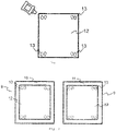
- Figure 1 shows a plain view of a bonding element 12, on which an adhesive 13 is applied.
- the adhesive 13 is applied to the four corners of the rectangular bonding element 12 in order to fix the bonding element 12 to a spacer 9 later on.
- the adhesive 13 can be an instantaneous glue, but also could be any other glue or paste having good adhesive properties on the surface of the bonding element 12 facing the spacers 9.
- the bonding element 12 consists of epoxy and can be reinforced with glass fibers to enhance the stability of the bonding elements 12. Under usual conditions, e.g. room temperature, the bonding element 12 is stiff. Thus, it becomes sticky under thermal processing. Therefore, the bonding elements 12 can be employed to bond to a conductor 6 by a thermal curing.
- Figure 2 shows a plain view of an upper surface 10 and a lower surface 11 of the spacer 9 after the bonding elements 12 have been adhered to the spacers 9 by the adhesive 13 dispensed at the corners of the bonding element 13.
- a safety distance of the bonding element 12 to the edges of the spacers 9 of at least 1 mm is maintained in order to avoid the adhesive 13 to be spilled on the conductor 6 later on, which could compromise the insulation of the conductor or of the winding.
- FIG 3 a plain view of the lower surface 11 of the spacer 9 is displayed, on which the adhesive 13 is applied in the middle of the bonding element 12.
- the spacer can be fixed to a no-adhesable upper surface 3 of the tape 2 by the adhesive 13 in the middle of the bonding element 12.
- the upper surface 3 of the tape 2 can be adhesable, for example by an adhesive layer, such that the spacers 9 can be fixed to the tape 2 without an additional adhesive 13 by arranging them directly on the tape 2.
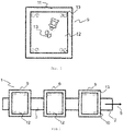
- Figure 4 shows a plain view of an embodiment of a spacer tape 1.
- the spacers 9 are adhered to the upper surface 3 of the tape 2 equidistantly.
- the distance between the spacers 9 along a longitudinal axis 5 of the tape 2 is a natural fraction of a circumference of a winding 8 as shown in figure 8 , the spacer tape 1 is used in. In this way, it is ensured that the spacers 9 are stacked on top of each other in the winding 8, whereby turns 7 of the winding 8 are positioned between them.
- the dimension of the bonding elements 13 in a direction perpendicular to the longitudinal axis 5 of tape 2 are larger than the dimension of the tape 2 in this direction.
- the bonding elements 13 protrude from the tape 2 on two sides. Therefore, after the spacer tape 2 is adhere to the conductor 6 as shown in figure 8 , the bonding elements 12 can bond directly to the conductor 6 at the area without tape 2, while being secured in position by the tape 2.
- the spacer tape 1 is shielded by a protective layer 15 which is arranged on the upper surface 11 of the spacer 9.
- the protective layer 15, which can be a plastic layer, conserves the adhesive property of the upper surface 11 of the spacer 9 from any dirt or dust. Moreover, protected by the protective layer 15, the spacer tape 1 can be easily transported.
- Figure 6 shows a plain view of a lower surface 11 of a spacer 9, on which an UV curable adhesive film 14, in contrary to the bonding element 12, is applied to make the lower surface 11 of the spacer 9 adhesable.
- the UV curable adhesive film 14 is fixed to the spacer by curing the UV curable adhesive film 14 just at the corners.
- the middle of the UV curable adhesive film 14 is omitted at this step to adhere the spacer 9 on the tape 2 over the UV curable adhesive film 14, as indicated in figure 7 .
- Figure 8 shows the winding 8 comprising the spacer tape 1.
- the spacer tape 1 has been adhered to the conductor 6, after which the conductor 7 was wound to form the turns 7 of the winding 8, such that the spacers 9 are arranged in between them to space the turns 7 apart. Thereafter, the whole winding 8 has been subjected to a thermal curing process, whereby the spacers 9 bond to both adjacent turns 7.
- the winding 8 is an integral electrical component formed by the conductor 6 and the spacer tape 1 that can withstand much larger electromagnetic forces compared to conventional spacers-type windings 8.
Landscapes
- Engineering & Computer Science (AREA)
- Power Engineering (AREA)
- Chemical & Material Sciences (AREA)
- Organic Chemistry (AREA)
- Manufacturing & Machinery (AREA)
- Insulating Of Coils (AREA)
- Coils Of Transformers For General Uses (AREA)
Priority Applications (5)
| Application Number | Priority Date | Filing Date | Title |
|---|---|---|---|
| EP21150953.4A EP4026879A1 (fr) | 2021-01-11 | 2021-01-11 | Bande d'espacement, procédé de fabrication d'un enroulement et enroulement |
| KR1020227046206A KR102799386B1 (ko) | 2021-01-11 | 2022-01-07 | 스페이서 테이프, 권선의 제조 방법 및 권선 |
| PCT/EP2022/050259 WO2022148834A1 (fr) | 2021-01-11 | 2022-01-07 | Ruban pour espaceur, procédé de fabrication d'un enroulement et enroulement |
| CN202280005312.4A CN115916915B (zh) | 2021-01-11 | 2022-01-07 | 间隔带、用于制造绕组的方法和绕组 |
| US17/928,563 US12512259B2 (en) | 2021-01-11 | 2022-01-07 | Spacer tape, method for manufacturing a winding and winding |
Applications Claiming Priority (1)
| Application Number | Priority Date | Filing Date | Title |
|---|---|---|---|
| EP21150953.4A EP4026879A1 (fr) | 2021-01-11 | 2021-01-11 | Bande d'espacement, procédé de fabrication d'un enroulement et enroulement |
Publications (1)
| Publication Number | Publication Date |
|---|---|
| EP4026879A1 true EP4026879A1 (fr) | 2022-07-13 |
Family
ID=74130124
Family Applications (1)
| Application Number | Title | Priority Date | Filing Date |
|---|---|---|---|
| EP21150953.4A Pending EP4026879A1 (fr) | 2021-01-11 | 2021-01-11 | Bande d'espacement, procédé de fabrication d'un enroulement et enroulement |
Country Status (5)
| Country | Link |
|---|---|
| US (1) | US12512259B2 (fr) |
| EP (1) | EP4026879A1 (fr) |
| KR (1) | KR102799386B1 (fr) |
| CN (1) | CN115916915B (fr) |
| WO (1) | WO2022148834A1 (fr) |
Citations (2)
| Publication number | Priority date | Publication date | Assignee | Title |
|---|---|---|---|---|
| WO2019238558A1 (fr) * | 2018-06-12 | 2019-12-19 | Asta Elektrodraht Gmbh | Conducteur parallèle multiple à plaquettes d'écartement |
| WO2021151610A1 (fr) * | 2020-01-30 | 2021-08-05 | Abb Power Grids Switzerland Ag | Procédé et structure de conducteur pour la fabrication d'un enroulement électrique d'un appareil à induction électromagnétique |
Family Cites Families (19)
| Publication number | Priority date | Publication date | Assignee | Title |
|---|---|---|---|---|
| GB551450A (en) | 1940-10-16 | 1943-02-23 | Westinghouse Electric Int Co | Improvements in or relating to insulated electrical conductors |
| DE3212060A1 (de) | 1982-04-01 | 1983-10-06 | Aeg Isolier Kunststoff | Flaechenisolierstoff fuer wicklungen aus aluminiumfolien, insbesondere fuer trockentransformatoren der temperaturklassen f und h |
| JPH069462Y2 (ja) * | 1988-05-13 | 1994-03-09 | 三菱電機株式会社 | 電磁誘導電器の巻線 |
| NL8802882A (nl) * | 1988-11-22 | 1990-06-18 | Smit Transformatoren Bv | Van axiale kanalen voorziene, als schijvenwikkeling uitgevoerde transformatorwikkeling. |
| SE512060C2 (sv) | 1997-02-03 | 2000-01-17 | Abb Ab | Lindning, förfarande för framställning av en sådan samt krafttransformator eller reaktor |
| JP2001143937A (ja) * | 1999-11-16 | 2001-05-25 | Hitachi Ltd | 変圧器巻線 |
| JP3462163B2 (ja) | 2000-08-18 | 2003-11-05 | ゴールド工業株式会社 | Tabテープ用スペーサテープ |
| JP2004115028A (ja) | 2002-09-24 | 2004-04-15 | Toppan Printing Co Ltd | テープ状半導体パッケージ基板用スペーサーテープ |
| JP5043340B2 (ja) | 2006-02-01 | 2012-10-10 | スリーエム イノベイティブ プロパティズ カンパニー | 物品取り付けキット |
| WO2011029488A1 (fr) | 2009-09-11 | 2011-03-17 | Abb Research Ltd | Transformateur comprenant un caloduc |
| WO2011126994A1 (fr) * | 2010-04-07 | 2011-10-13 | Abb Technology Ag | Transformateur torique à enroulement discoïde |
| JP2013010901A (ja) | 2011-06-30 | 2013-01-17 | Hitachi Chemical Co Ltd | ロール状に巻かれた形状付きフィルム及びその製造方法 |
| DE102012223366A1 (de) | 2012-12-17 | 2014-06-18 | Siemens Aktiengesellschaft | Supraleitende Spuleneinrichtung mit Spulenwicklung und Kontakten |
| CN106463217B (zh) | 2014-04-14 | 2018-07-06 | Abb瑞士股份有限公司 | 制造高电压构件的高电压绝缘间隔件的方法和包括根据该方法制造的间隔件的高电压构件 |
| WO2016073576A1 (fr) | 2014-11-04 | 2016-05-12 | SAHIN, Hakan | Systèmes et procédés relatifs à un transformateur électrique |
| CN205122221U (zh) | 2015-08-07 | 2016-03-30 | 阿斯塔导线有限公司 | 低环氧轴向油道网包换位导线 |
| DE102017208814A1 (de) | 2017-05-24 | 2018-11-29 | Isotek Gmbh | Distanzband, Transformatorenwicklung und Transformator sowie das Verfahren zur Herstellung eines Distanzbandes |
| FR3081259B1 (fr) | 2018-05-17 | 2022-01-28 | Inst Supergrid | Limiteur de courant supraconducteur avec entretoise electriquement conductrice |
| SE1951171A1 (en) * | 2019-10-16 | 2019-10-16 | Abb Schweiz Ag | Clackband, electric transformer and method |
-
2021
- 2021-01-11 EP EP21150953.4A patent/EP4026879A1/fr active Pending
-
2022
- 2022-01-07 WO PCT/EP2022/050259 patent/WO2022148834A1/fr not_active Ceased
- 2022-01-07 KR KR1020227046206A patent/KR102799386B1/ko active Active
- 2022-01-07 US US17/928,563 patent/US12512259B2/en active Active
- 2022-01-07 CN CN202280005312.4A patent/CN115916915B/zh active Active
Patent Citations (2)
| Publication number | Priority date | Publication date | Assignee | Title |
|---|---|---|---|---|
| WO2019238558A1 (fr) * | 2018-06-12 | 2019-12-19 | Asta Elektrodraht Gmbh | Conducteur parallèle multiple à plaquettes d'écartement |
| WO2021151610A1 (fr) * | 2020-01-30 | 2021-08-05 | Abb Power Grids Switzerland Ag | Procédé et structure de conducteur pour la fabrication d'un enroulement électrique d'un appareil à induction électromagnétique |
Non-Patent Citations (2)
| Title |
|---|
| ANONYMOUS: "Adhesable - Definition and More from the Free Merriam-Webster Dictionary", MERRIAM WEBSTER ONLINE DICTIONARY, 28 May 2021 (2021-05-28), pages 1 - 5, XP055808585, Retrieved from the Internet <URL:https://www.merriam-webster.com/dictionary/adhesable> [retrieved on 20210528] * |
| ANONYMOUS: "Neologism", WIKIPEDIA, 19 July 2021 (2021-07-19), pages 1 - 6, XP055831640, Retrieved from the Internet <URL:https://en.wikipedia.org/wiki/Neologism> [retrieved on 20210811] * |
Also Published As
| Publication number | Publication date |
|---|---|
| CN115916915A (zh) | 2023-04-04 |
| US20230215620A1 (en) | 2023-07-06 |
| KR102799386B1 (ko) | 2025-04-22 |
| KR20230017874A (ko) | 2023-02-06 |
| CN115916915B (zh) | 2024-08-09 |
| WO2022148834A1 (fr) | 2022-07-14 |
| US12512259B2 (en) | 2025-12-30 |
Similar Documents
| Publication | Publication Date | Title |
|---|---|---|
| JP4735529B2 (ja) | モータの固定子 | |
| KR101483379B1 (ko) | 전선 보호 구조부 및 전선 보호 구조부의 제조 방법 | |
| US8760029B2 (en) | Stator core arrangements using heat-shrinkable tubing, for rotarty electric machines | |
| US20070193767A1 (en) | Electricity transport conductor for overhead lines | |
| US7365465B2 (en) | Securing assembly of bandages for synchronous motors with outer permanent magnets | |
| JP2010137527A (ja) | 複合材料の修理方法 | |
| CN108695037B (zh) | 用于在超导磁体中支撑结构的线圈连接 | |
| US9385346B2 (en) | Organic light emitting diode display panel and method for manufacturing the same | |
| US20080118215A1 (en) | Light tunnel structure and manufacturing method thereof | |
| US12512259B2 (en) | Spacer tape, method for manufacturing a winding and winding | |
| JP5471285B2 (ja) | ステータ、ロータ、および超電導機器 | |
| EP0116367B1 (fr) | Enroulement conducteur de courant et procédé de fabrication de celui-ci | |
| KR100883698B1 (ko) | 인덕터 및 인덕터 제조방법 | |
| US20240278900A1 (en) | Panel skin for heated floor panels | |
| CN107968500B (zh) | 磁极模块、其制造方法、转子及电机 | |
| CN108773120B (zh) | 高强度芳纶纸夹芯复合结构及其制造方法 | |
| KR20140112028A (ko) | 변압기 코어 | |
| JP2006135060A (ja) | 超電導マグネットおよびその製造方法 | |
| KR20200045756A (ko) | 영구자석을 이용한 전기모터용 회전자의 제조방법 및 이러한 방법으로 제조된 영구자석을 이용한 전기모터용 회전자 | |
| CN117957752A (zh) | 旋转机线圈、其制造方法及旋转机 | |
| EP3859760A1 (fr) | Procede et structure conductrice pour la fabrication d'un enroulement electrique d'un appareil a induction electromagnetique | |
| CN109962588B (zh) | 转子的制造方法、转子的修复方法、转子和电机 | |
| US20230343509A1 (en) | Structural arrangement for mounting conductor winding packages in air core reactor | |
| JP5663322B2 (ja) | 樹脂モールドコイル、及びそれを用いたモールド変圧器 | |
| KR20210070067A (ko) | 모터 |
Legal Events
| Date | Code | Title | Description |
|---|---|---|---|
| PUAI | Public reference made under article 153(3) epc to a published international application that has entered the european phase |
Free format text: ORIGINAL CODE: 0009012 |
|
| STAA | Information on the status of an ep patent application or granted ep patent |
Free format text: STATUS: THE APPLICATION HAS BEEN PUBLISHED |
|
| AK | Designated contracting states |
Kind code of ref document: A1 Designated state(s): AL AT BE BG CH CY CZ DE DK EE ES FI FR GB GR HR HU IE IS IT LI LT LU LV MC MK MT NL NO PL PT RO RS SE SI SK SM TR |
|
| RIN1 | Information on inventor provided before grant (corrected) |
Inventor name: PLATEK, ROBERT Inventor name: GIRLANDA, ORLANDO Inventor name: JOVALEKIC, MARK Inventor name: FORSLIN, JULIA Inventor name: VALORI, VALENTINA Inventor name: PAVANELLO, PAOLO Inventor name: PERIN, MARTINA Inventor name: BUSTREO, GIANLUCA |
|
| STAA | Information on the status of an ep patent application or granted ep patent |
Free format text: STATUS: REQUEST FOR EXAMINATION WAS MADE |
|
| 17P | Request for examination filed |
Effective date: 20230105 |
|
| RBV | Designated contracting states (corrected) |
Designated state(s): AL AT BE BG CH CY CZ DE DK EE ES FI FR GB GR HR HU IE IS IT LI LT LU LV MC MK MT NL NO PL PT RO RS SE SI SK SM TR |
|
| P01 | Opt-out of the competence of the unified patent court (upc) registered |
Effective date: 20230527 |
|
| RAP1 | Party data changed (applicant data changed or rights of an application transferred) |
Owner name: HITACHI ENERGY LTD |