EP4027400A1 - Dispositif électroluminescent organique - Google Patents
Dispositif électroluminescent organique Download PDFInfo
- Publication number
- EP4027400A1 EP4027400A1 EP22150279.2A EP22150279A EP4027400A1 EP 4027400 A1 EP4027400 A1 EP 4027400A1 EP 22150279 A EP22150279 A EP 22150279A EP 4027400 A1 EP4027400 A1 EP 4027400A1
- Authority
- EP
- European Patent Office
- Prior art keywords
- group
- substituted
- unsubstituted
- salt
- phenyl
- Prior art date
- Legal status (The legal status is an assumption and is not a legal conclusion. Google has not performed a legal analysis and makes no representation as to the accuracy of the status listed.)
- Pending
Links
Images
Classifications
-
- H—ELECTRICITY
- H10—SEMICONDUCTOR DEVICES; ELECTRIC SOLID-STATE DEVICES NOT OTHERWISE PROVIDED FOR
- H10K—ORGANIC ELECTRIC SOLID-STATE DEVICES
- H10K85/00—Organic materials used in the body or electrodes of devices covered by this subclass
- H10K85/40—Organosilicon compounds, e.g. TIPS pentacene
-
- H—ELECTRICITY
- H10—SEMICONDUCTOR DEVICES; ELECTRIC SOLID-STATE DEVICES NOT OTHERWISE PROVIDED FOR
- H10K—ORGANIC ELECTRIC SOLID-STATE DEVICES
- H10K50/00—Organic light-emitting devices
- H10K50/10—OLEDs or polymer light-emitting diodes [PLED]
- H10K50/11—OLEDs or polymer light-emitting diodes [PLED] characterised by the electroluminescent [EL] layers
-
- H—ELECTRICITY
- H10—SEMICONDUCTOR DEVICES; ELECTRIC SOLID-STATE DEVICES NOT OTHERWISE PROVIDED FOR
- H10K—ORGANIC ELECTRIC SOLID-STATE DEVICES
- H10K85/00—Organic materials used in the body or electrodes of devices covered by this subclass
- H10K85/60—Organic compounds having low molecular weight
- H10K85/615—Polycyclic condensed aromatic hydrocarbons, e.g. anthracene
-
- H—ELECTRICITY
- H10—SEMICONDUCTOR DEVICES; ELECTRIC SOLID-STATE DEVICES NOT OTHERWISE PROVIDED FOR
- H10K—ORGANIC ELECTRIC SOLID-STATE DEVICES
- H10K85/00—Organic materials used in the body or electrodes of devices covered by this subclass
- H10K85/60—Organic compounds having low molecular weight
- H10K85/649—Aromatic compounds comprising a hetero atom
- H10K85/654—Aromatic compounds comprising a hetero atom comprising only nitrogen as heteroatom
-
- H—ELECTRICITY
- H10—SEMICONDUCTOR DEVICES; ELECTRIC SOLID-STATE DEVICES NOT OTHERWISE PROVIDED FOR
- H10K—ORGANIC ELECTRIC SOLID-STATE DEVICES
- H10K85/00—Organic materials used in the body or electrodes of devices covered by this subclass
- H10K85/60—Organic compounds having low molecular weight
- H10K85/649—Aromatic compounds comprising a hetero atom
- H10K85/657—Polycyclic condensed heteroaromatic hydrocarbons
- H10K85/6572—Polycyclic condensed heteroaromatic hydrocarbons comprising only nitrogen in the heteroaromatic polycondensed ring system, e.g. phenanthroline or carbazole
-
- H—ELECTRICITY
- H10—SEMICONDUCTOR DEVICES; ELECTRIC SOLID-STATE DEVICES NOT OTHERWISE PROVIDED FOR
- H10K—ORGANIC ELECTRIC SOLID-STATE DEVICES
- H10K85/00—Organic materials used in the body or electrodes of devices covered by this subclass
- H10K85/60—Organic compounds having low molecular weight
- H10K85/649—Aromatic compounds comprising a hetero atom
- H10K85/657—Polycyclic condensed heteroaromatic hydrocarbons
- H10K85/6574—Polycyclic condensed heteroaromatic hydrocarbons comprising only oxygen in the heteroaromatic polycondensed ring system, e.g. cumarine dyes
-
- H—ELECTRICITY
- H10—SEMICONDUCTOR DEVICES; ELECTRIC SOLID-STATE DEVICES NOT OTHERWISE PROVIDED FOR
- H10K—ORGANIC ELECTRIC SOLID-STATE DEVICES
- H10K2101/00—Properties of the organic materials covered by group H10K85/00
- H10K2101/10—Triplet emission
-
- H—ELECTRICITY
- H10—SEMICONDUCTOR DEVICES; ELECTRIC SOLID-STATE DEVICES NOT OTHERWISE PROVIDED FOR
- H10K—ORGANIC ELECTRIC SOLID-STATE DEVICES
- H10K2101/00—Properties of the organic materials covered by group H10K85/00
- H10K2101/30—Highest occupied molecular orbital [HOMO], lowest unoccupied molecular orbital [LUMO] or Fermi energy values
-
- H—ELECTRICITY
- H10—SEMICONDUCTOR DEVICES; ELECTRIC SOLID-STATE DEVICES NOT OTHERWISE PROVIDED FOR
- H10K—ORGANIC ELECTRIC SOLID-STATE DEVICES
- H10K50/00—Organic light-emitting devices
- H10K50/10—OLEDs or polymer light-emitting diodes [PLED]
- H10K50/11—OLEDs or polymer light-emitting diodes [PLED] characterised by the electroluminescent [EL] layers
- H10K50/12—OLEDs or polymer light-emitting diodes [PLED] characterised by the electroluminescent [EL] layers comprising dopants
-
- H—ELECTRICITY
- H10—SEMICONDUCTOR DEVICES; ELECTRIC SOLID-STATE DEVICES NOT OTHERWISE PROVIDED FOR
- H10K—ORGANIC ELECTRIC SOLID-STATE DEVICES
- H10K85/00—Organic materials used in the body or electrodes of devices covered by this subclass
- H10K85/60—Organic compounds having low molecular weight
- H10K85/649—Aromatic compounds comprising a hetero atom
- H10K85/657—Polycyclic condensed heteroaromatic hydrocarbons
Definitions
- the present disclosure relates to an organic light-emitting device.
- OLEDs Organic light-emitting devices
- OLEDs are self-emissive devices which produce full-color images.
- OLEDs have wide viewing angles and exhibit excellent driving voltage and response speed characteristics.
- OLEDs include an anode, a cathode, and an organic layer between the anode and the cathode and including an emission layer.
- a hole transport region may be between the anode and the emission layer, and an electron transport region may be between the emission layer and the cathode.
- Holes provided from the anode may move toward the emission layer through the hole transport region, and electrons provided from the cathode may move toward the emission layer through the electron transport region.
- the holes and the electrons recombine in the emission layer to produce excitons.
- the excitons may transition from an excited state to a ground state, thus generating visible light.
- an organic light-emitting device including a silane compound as a host, thus having high efficiency, long lifespan, and high triplet-triplet fusion (TTF) ratio characteristics.
- TTF triplet-triplet fusion
- an organic light-emitting device may include:
- Ar 1 to Ar 3 may each independently be a substituted or unsubstituted C 1 -C 60 alkyl group, a substituted or unsubstituted C 2 -C 60 alkenyl group, a substituted or unsubstituted C 2 -C 60 alkynyl group, a substituted or unsubstituted C 1 -C 60 alkoxy group, a substituted or unsubstituted C 1 -C 60 alkylthio group, a substituted or unsubstituted C 3 -C 10 cycloalkyl group, a substituted or unsubstituted C 1 -C 10 heterocycloalkyl group, a substituted or unsubstituted C 3 -C 10 cycloalkenyl group, a substituted or unsubstituted C 1 -C 10 heterocycloalkenyl group, a substituted or unsubstituted C 6 -C 60 aryl group, a substituted or un
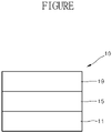
- FIGURE shows a schematic cross-sectional view of an organic light-emitting device according to an embodiment.
- first, second, third etc. may be used herein to describe various elements, components, regions, layers, and/or sections, these elements, components, regions, layers, and/or sections should not be limited by these terms. These terms are only used to distinguish one element, component, region, layer, or section from another element, component, region, layer, or section. Thus, a first element, component, region, layer, or section discussed below could be termed a second element, component, region, layer, or section without departing from the teachings of the present embodiments.
- Exemplary embodiments are described herein with reference to cross section illustrations that are schematic illustrations of idealized embodiments. As such, variations from the shapes of the illustrations as a result, for example, of manufacturing techniques and/or tolerances, are to be expected. Thus, embodiments described herein should not be construed as limited to the particular shapes of regions as illustrated herein but are to include deviations in shapes that result, for example, from manufacturing. For example, a region illustrated or described as flat may, typically, have rough and/or nonlinear features. Moreover, sharp angles that are illustrated may be rounded. Thus, the regions illustrated in the figures are schematic in nature and their shapes are not intended to illustrate the precise shape of a region and are not intended to limit the scope of the present claims.
- * and *' each indicate a binding site to a neighboring atom or a neighboring functional group.
- room temperature refers to a temperature of about 25 °C.
- a silane compound represented by Formula 1 may be provided:
- Ar 1 to Ar 3 may each independently be:
- At least one of Ar 1 to Ar 3 may be:
- Ar 1 to Ar 3 may each independently be a substituted or unsubstituted C 6 -C 60 aryl group, a substituted or unsubstituted C 1 -C 60 heteroaryl group, a substituted or unsubstituted monovalent non-aromatic condensed polycyclic group, or a substituted or unsubstituted monovalent non-aromatic condensed heteropolycyclic group.
- Ar 1 to Ar 3 may each independently be: a cyclopentyl group, a cyclohexyl group, a cyclopentenyl group, a cyclohexenyl group, a cycloheptenyl group, a phenyl group, a pentalenyl group, an indenyl group, a naphthyl group, an azulenyl group, a heptalenyl group, an indacenyl group, an acenaphthyl group, a fluorenyl group, a spiro-bifluorenyl group, a phenalenyl group, a phenanthrenyl group, an anthracenyl group, a fluoranthenyl group, a triphenylenyl group, a pyrenyl group, a chrysenyl group, a naphthacenyl group, a piceny
- Ar 1 to Ar 3 may each independently be:
- L 10 may be a substituted or unsubstituted C 5 -C 30 carbocyclic group or a substituted or unsubstituted C 1 -C 30 heterocyclic group.
- L 10 may be: a phenylene group, a pentalenylene group, an indenylene group, a naphthylene group, an azulenylene group, a heptalenylene group, an acenaphthylene group, a fluorenylene group, a phenalenylene group, a phenanthrenylene group, an anthracenylene group, a fluoranthenylene group, a triphenylenylene group, a pyrenylene group, a chrysenylenylene group, a naphthacenylene group, a picenylene group, a perylenylene group, a pentacenylene group, a carbazolylene group, a dibenzofuranylene group, a dibenzothiophenylene group, a dibenzosilolylene group, a benzocarbazolylene group, a pyridiny
- Y 21 to Y 24 may each independently be a single bond, O, S, N(R 21 ), C(R 21 )(R 22 ), or Si(R 21 )(R 22 ).
- Y 21 and Y 22 may not each be a single bond simultaneously, and Y 23 and Y 24 may not each be a single bond simultaneously.
- a 21 to A 23 may each independently be a phenyl group, a naphthalene group, a pyridine group, or a pyrimidine group.
- a 21 to A 23 may each independently be a phenyl group or a naphthalene group.
- a10 may be an integer from 0 to 3, and when a10 is 2 or greater, at least two L 10 (s) may be identical to or different from each other.
- a10 may be 0 or 1.
- a10 may be 0.
- a10 may be 1.
- a10 - represents a single bond.
- R 10 and R 20 may each independently be hydrogen, deuterium, - F, -CI, -Br, -I, -SF 5 , a hydroxyl group, a cyano group, a nitro group, an amidino group, a hydrazine group, a hydrazone group, a carboxylic acid group or a salt thereof, a sulfonic acid group or a salt thereof, a phosphoric acid group or a salt thereof, a substituted or unsubstituted C 1 -C 60 alkyl group, a substituted or unsubstituted C 2 -C 60 alkenyl group, a substituted or unsubstituted C 2 -C 60 alkynyl group, a substituted or unsubstituted C 1 -C 60 alkoxy group, a substituted or unsubstituted C 1 -C 60 alkylthio group, a substituted or unsubstituted C 3 -
- R 10 and R 20 may each independently be:
- R 10 and R 20 may each independently be: hydrogen, deuterium, -F, -CI, -Br, -I, a hydroxyl group, a cyano group, a nitro group, an amino group, an amidino group, a hydrazine group, a hydrazone group, a carboxylic acid group or a salt thereof, a sulfonic acid group or a salt thereof, a phosphoric acid group or a salt thereof, a C 1 -C 20 alkyl group, a C 1 -C 20 alkylthio group, or a C 1 -C 20 alkoxy group;
- R 10 and R 20 may each independently be deuterium, -F, a cyano group, -CD 3 , -CD 2 H, -CDH 2 , -CF 3 , -CF 2 H, -CFH 2 , groups represented by Formulae 9-1 to 9-19, or groups represented by Formulae10-1 to 10-211: wherein, in Formulae 9-1 to 9-19 and 10-1 to 10-211, * indicates a binding site to an adjacent atom, "Ph” represents a phenyl group, and "TMS" represents a trimethylsilyl group.
- R 10 and R 20 may each independently be: hydrogen, deuterium, -F, a cyano group, -CD 3 , -CD 2 H, -CDH 2 , -CF 3 , -CF 2 H, -CFH 2 , a C 1 -C 20 alkyl group, a C 1 -C 20 alkylthio group, or a C 1 -C 20 alkoxy group;
- R 10 may be: deuterium, -F, a cyano group, -CD 3 , -CD 2 H, - CDH 2 , -CF 3 , -CF 2 H, -CFH 2 , a C 1 -C 20 alkyl group, a C 1 -C 20 alkylthio group, or a C 1 -C 20 alkoxy group;
- R 20 may be hydrogen, deuterium, -F, a cyano group, -CD 3 , -CD 2 H, -CDH 2 , -CF 3 , -CF 2 H, -CFH 2 , a C 1 -C 20 alkyl group, or a phenyl group.
- b10 and b20 may each independently be an integer from 1 to 8. When b10 is 2 or greater, at least two R 10 (s) may be identical to or different from each other. When b20 is 2 or greater, at least two R 20 (s) may be identical to or different from each other.
- b10 and b20 may each independently be 1, 2, 3, or 4.
- b10 may be 1.
- b20 may be 1.
- c10 may be an integer from 1 to 9. When c10 is 2 or greater, at least two -[(L 10 ) a10 -(R 10 ) b10 ] group(s) may be identical to or different from each other.
- c10 may be 1, 2, 3, or 4.
- c10 may be 1 or 2.
- c10 may be 1.
- a sum of b20 and c10 may be 9.
- silane compound represented by Formula 1 may be represented by one of Formulae 10-1 to 10-5:
- the silane compound represented by Formula 1 may be a compound represented by Formula 10-5.
- R 10 may be: a C 1 -C 20 alkyl group, a C 1 -C 20 alkylthio group, or a C 1 -C 20 alkoxy group;
- the silane compound may be one of Compounds 1 to 160:
- the silane compound represented by Formula 1 may have an asymmetric structure, it may have a low crystallinity of a material. In an embodiment, as intermolecular close packing of the silane compound represented by Formula 1 may be prevented, the silane compound may have relatively excellent or improved amorphous thin film characteristics.
- the silane compound represented by Formula 1 may have suitable electrical characteristics for a material for organic light-emitting devices, e.g., a host material, a hole transport material, and an electron transport material in an emission layer.
- a material for organic light-emitting devices e.g., a host material, a hole transport material, and an electron transport material in an emission layer.
- an organic light-emitting device including the silane compound may have high or improved efficiency and/or a long or improved lifespan.
- the silane compound represented by Formula 1 may satisfy Equation 1: E T1 ⁇ E S1 ⁇ 2 ⁇ E T1 wherein, in Equation 1, E(T1) indicates a lowest excited triplet energy level of the silane compound, and E(S1) indicates a lowest excited singlet energy level of the silane compound.
- the silane compound represented by Formula 1 may satisfy Equation 2: 2 ⁇ E T 1 ⁇ E S 1 ⁇ 1 eV wherein, in Equation 2, E(T1) indicates a lowest excited triplet energy level of the silane compound, and E(S1) indicates a lowest excited singlet energy level of the silane compound.
- TTF triplet-triplet fusion
- the silane compound represented by Formula 1 may satisfy Equation 2-1: 2 ⁇ E T 1 ⁇ E S 1 ⁇ 0.5 eV wherein, in Equation 2-1, E(T1) indicates a lowest excited triplet energy level of the silane compound, and E(S1) indicates a lowest excited singlet energy level of the silane compound.
- a method of synthesizing the silane compound represented by Formula 1 may be apparent to one of ordinary skill in the art by referring to Synthesis Examples provided herein.
- an organic light-emitting device may include: a first electrode; a second electrode; and an organic layer between the first electrode and the second electrode, the organic layer including an emission layer and at least one of the silane compound represented by Formula 1.
- the organic light-emitting device has an organic layer including the silane compound represented by Formula 1, the organic light-emitting device may have a low driving voltage, high or improved efficiency, high or improved luminance, high or improved quantum efficiency, and long or improved lifespan.
- the emission layer in the organic light-emitting device may include at least one of the silane compounds represented by Formula 1.
- the emission layer in the organic light-emitting device may include a host and a dopant, wherein the host may include at least one of the silane compound represented by Formula 1, and the dopant may include a phosphorescent dopant or a fluorescent dopant.
- the dopant may include a phosphorescent dopant (e.g., an organometallic compound represented by Formula 81 provided herein).
- the host may further include any suitable host, in addition to the silane compound represented by Formula 1.
- the emission layer may emit red light, green light, or blue light.
- the emission layer may include a fluorescent dopant, but embodiments are not limited thereto.
- the emission layer may include a phosphorescent dopant, but embodiments are not limited thereto.
- the silane compound represented by Formula 1 may be included in a hole transport region of the organic light-emitting device.
- a hole transport region of the organic light-emitting device may include at least one of a hole injection layer, a hole transport layer, or an electron blocking layer, wherein at least one of the hole injection layer, the hole transport layer, or the electron blocking layer may include the silane compound represented by Formula 1.
- the silane compound represented by Formula 1 may be included in an electron transport region of the organic light-emitting device.
- an electron transport region of the organic light-emitting device may include at least one of a hole blocking layer, an electron transport layer, or an electron injection layer, wherein at least one of the hole blocking layer, the electron transport layer, or the electron injection layer, may include the silane compound represented by Formula 1.
- a hole transport region of the organic light-emitting device may include an electron blocking layer, wherein the electron blocking layer may include the silane compound represented by Formula 1.
- the electron blocking layer may be in a direct contact with the emission layer.
- an electron transport region of the organic light-emitting device may include a hole blocking layer, wherein the hole blocking layer may include the silane compound represented by Formula 1.
- the hole blocking layer may be in a direct contact with the emission layer.
- an organic light-emitting device may include: a first electrode; a second electrode; and an organic layer between the first electrode and the second electrode and including an emission layer, wherein the emission layer may include a host and a dopant, and the host may include at least one silane compound represented by Formula 1.
- a content of the host may be greater than a content of the dopant in the emission layer in the organic light-emitting device.
- the host in the emission layer in the organic light-emitting device may consist of the silane compound.
- a ratio of emission components emitted from the dopant may be 80% or greater of the whole emission components emitted from the emission layer of the organic light-emitting device.
- the dopant in the emission layer in the organic light-emitting device may be a fluorescent dopant.
- the fluorescent dopant may be a condensed polycyclic compound or a styryl-based compound.
- the fluorescent dopant may include a naphthalene-containing core, a fluorene-containing core, a spiro-bifluorene-containing core, a benzofluorene-containing core, a dibenzofluorene-containing core, a phenanthrene-containing core, an anthracene-containing core, a fluoranthene-containing core, a triphenylene-containing core, a pyrene-containing core, a chrysene-containing core, a naphthacene-containing core, a picene-containing core, a perylene-containing core, a pentaphene-containing core, an indenoanthracene-containing core, a tetracene-containing core, a bisanthracene-containing core, or a core represented by one of Formulae 501-1 to 501-18, but embodiments are not limited thereto:
- the fluorescent dopant may be a styryl-amine-based compound or a styryl-carbazole-based compound, but embodiments are not limited thereto.
- the fluorescent dopant may be compounds represented by Formula 501: wherein, in Formula 501,
- Ar 501 may be:
- the fluorescent dopant may include a compound represented by one of Formulae 502-1 to 502-5: wherein, in Formulae 502-1 to 502-5,
- the fluorescent dopant may include, for example, Compounds FD(1) to FD(16) or FD1 to FD13:
- the emission layer in the organic light-emitting device may further include a phosphorescent dopant, in addition to the silane compound represented by Formula 1.
- the phosphorescent dopant may include an organometallic compound represented by Formula 81: Formula 81 M(L 81 ) n81 (L 82 ) n82 wherein L 81 may be a ligand represented by Formula 81A, wherein, in Formulae 81 and 81A,
- Y 81 may be N, Y 82 to Y 84 may each be C, CY 81 may be 5-membered rings including two N atoms as ring-forming atoms, and CY 82 may be a phenyl group, a naphthalene group, a fluorene group, a dibenzofuran group, or a dibenzothiophene group, but embodiments are not limited thereto.
- Y 81 may be N, Y 82 to Y 84 may each be C, CY 81 may be an imidazole group or a 2,3-dihydro-1H-imidazole group, and CY 82 may be a phenyl group, a naphthalene group, a fluorene group, a dibenzofuran group, or a dibenzothiophene group, but embodiments are not limited thereto.
- R 81 and R 82 may each independently be:
- At least one of R 81 (s) in the number of a81 and R 82 (s) in the number of a82 may be a cyano group.
- At least one of R 82 (s) in the number of a82 may be a cyano group.
- At least one of R 81 (s) in the number of a81 and R 82 (s) in the number of a82 may be deuterium.
- L 82 may be ligands represented by Formulae one of 3-1(1) to 3-1(69), 3-1(71) to 3-1(79), 3-1(81) to 3-1(88), 3-1(91) to 3-1(98), and 3-1(101) to 3-1(114):
- M may be Ir, and a sum of n81 and n82 may be 3. In an embodiment, in Formula 81, M may be Pt, and a sum of n81 and n82 may be 2.
- the organometallic compound represented by Formula 81 may be neutral and may not include ion pairs of cations and anions.
- the organometallic compound represented by Formula 81 may include at least one of Compounds PD1 to PD78 or Flr 6 , but embodiments are not limited thereto:
- the emission layer in the light-emitting device may emit blue light having a maximum emission wavelength in a range of about 410 nanometers (nm) to about 490 nm.
- the expression the "(organic layer) includes at least one silane compound represented by Formula 1" may be construed as meaning the "(organic layer) may include one silane compound represented by Formula 1 or two or more different silane compounds represented by Formula 1".
- Compound 1 may only be included as the silane compound in the organic layer.
- Compound 1 may be included in the emission layer of the organic light-emitting device.
- the organic layer may include Compounds 1 and 2 as the silane compounds.
- Compounds 1 and 2 may be present in the same layer (for example, Compounds 1 and 2 may be both present in an emission layer), or in different layers (for example, Compound 1 may be present in an emission layer, and Compound 2 may be present in a hole blocking layer).
- the first electrode may be an anode, which is a hole injection electrode
- the second electrode may be a cathode, which is an electron injection electrode
- the first electrode may be a cathode, which is an electron injection electrode
- the second electrode may be an anode, which is a hole injection electrode.
- organic layer refers to a single and/or a plurality of layers between the first electrode and the second electrode in an organic light-emitting device.
- the “organic layer” may include not only organic compounds but also organometallic complexes including metals.
- the FIGURE illustrates a schematic cross-sectional view of an organic light-emitting device 10 according to an embodiment.
- the organic light-emitting device 10 may include a first electrode 11, an organic layer 15, and a second electrode 19, which may be sequentially layered in this stated order.
- a substrate may be additionally disposed under the first electrode 11 or on the second electrode 19.
- the substrate may be any suitable substrate used in organic light-emitting devices, e.g., a glass substrate or a transparent plastic substrate, each having excellent mechanical strength, thermal stability, transparency, surface smoothness, ease of handling, and water repellency.
- the first electrode 11 may be formed by depositing or sputtering, onto the substrate, a material for forming the first electrode 11.
- the first electrode 11 may be an anode.
- the material for forming the first electrode 11 may be materials with a high work function for easy hole injection.
- the first electrode 11 may be a reflective electrode, a semi-transmissive electrode, or a transmissive electrode.
- the material for forming the first electrode 11 may be indium tin oxide (ITO), indium zinc oxide (IZO), tin oxide (SnO 2 ), or zinc oxide (ZnO).
- the material for forming the first electrode 11 may be a metal, such as magnesium (Mg), aluminum (Al), aluminum-lithium (Al-Li), calcium (Ca), magnesium-indium (Mg-In), or magnesium-silver (Mg-Ag).
- Mg magnesium
- Al aluminum
- Al-Li aluminum-lithium
- Ca calcium
- Mg-In magnesium-indium
- Mg-Ag magnesium-silver
- the first electrode 11 may have a single-layered structure or a multi-layered structure including a plurality of layers. In an embodiment, the first electrode 11 may have a triple-layered structure of ITO/Ag/ITO, but embodiments are not limited thereto.
- the organic layer 15 may be on the first electrode 11.
- the organic layer 15 may include a hole transport region, an emission layer, and an electron transport region.
- the hole transport region may be between the first electrode 11 and the emission layer.
- the hole transport region may include at least one of a hole injection layer, a hole transport layer, an electron blocking layer, or a buffer layer.
- the hole transport region may include a hole injection layer only or a hole transport layer only. In an embodiment, the hole transport region may include a hole injection layer and a hole transport layer which are sequentially stacked on the first electrode 11. In an embodiment, the hole transport region may include a hole injection layer, a hole transport layer, and an electron blocking layer, which are sequentially stacked on the first electrode 11.
- the hole injection layer may be formed on the first electrode 11 by using one or more suitable methods, such as vacuum deposition, spin coating, casting, and Langmuir-Blodgett (LB) deposition.
- suitable methods such as vacuum deposition, spin coating, casting, and Langmuir-Blodgett (LB) deposition.
- the vacuum deposition may be performed at a temperature in a range of about 100°C to about 500°C, at a vacuum degree in a range of about 10 -8 torr to about 10 -3 torr, and at a rate in a range of about 0.01 Angstroms per second ( ⁇ /sec) to about 100 ⁇ /sec, though the conditions may vary depending on a compound used as a hole injection material and a structure and thermal properties of a desired hole injection layer, but embodiments are not limited thereto.
- the spin coating may be performed at a rate in a range of about 2,000 revolutions per minute (rpm) to about 5,000 rpm and at a temperature in a range of about 80°C to 200°C to facilitate removal of a solvent after the spin coating, though the conditions may vary depending on a compound used as a hole injection material and a structure and thermal properties of a desired hole injection layer, but embodiments are not limited thereto.
- the conditions for forming a hole transport layer and an electron blocking layer may be inferred from the conditions for forming the hole injection layer.
- the hole transport region may include at least one of m-MTDATA, TDATA, 2-TNATA, NPB, ⁇ -NPB, TPD, spiro-TPD, spiro-NPB, methylated NPB, TAPC, HMTPD, 4,4',4"-tris(N-carbazolyl)triphenylamine (TCTA), polyaniline/dodecylbenzenesulfonic acid (PANI/DBSA), poly(3,4-ethylenedioxythiophene)/poly(4-styrenesulfonate) (PEDOT/PSS), polyaniline/camphor sulfonic acid (PANI/CSA), (polyaniline)/poly(4-styrenesulfonate) (PANI/PSS), a compound represented by Formula 201, or a compound represented by Formula 202: wherein, in Formula 201, Ar 101 and Ar 102 may each independently be:
- xa and xb may each independently be an integer from 0 to 5. In an embodiment, xa and xb may each independently be 0, 1, or 2. In an embodiment, xa may be 1, and xb may be 0, but embodiments are not limited thereto.
- R 101 to R 108 , R 111 to R 119 , and R 121 to R 124 may each independently be:
- R 109 may be:
- the compound represented by Formula 201 may be represented by Formula 201A, but embodiments are not limited thereto: wherein, in Formula 201A, R 101 , R 111 , R 112 , and R 109 may respectively be understood by referring to the descriptions of R 101 , R 111 , R 112 , and R 109 provided herein.
- the compounds represented by Formulae 201 and 202 may include Compounds HT1 to HT20, but embodiments are not limited thereto:
- the thickness of the hole transport region may be in a range of about 100 Angstroms ( ⁇ ) to about 10,000 ⁇ , for example, about 100 ⁇ to about 1,000 ⁇ , about 100 ⁇ to about 2,000 ⁇ , about 100 ⁇ to about 3,000 ⁇ , about 100 ⁇ to about 4,000 ⁇ , about 100 ⁇ to about 5,000 ⁇ , about 100 ⁇ to about 6,000 ⁇ , about 100 ⁇ to about 7,000 ⁇ , about 100 ⁇ to about 8,000 ⁇ , or about 100 ⁇ to about 9,000 ⁇ .
- the thickness of the hole injection layer may be in a range of about 100 ⁇ to about 10,000 ⁇ , for example, about 100 ⁇ to about 1,000 ⁇ , 100 ⁇ to about 2,000 ⁇ , about 100 ⁇ to about 3,000 ⁇ , about 100 ⁇ to about 4,000 ⁇ , about 100 ⁇ to about 5,000 ⁇ , about 100 ⁇ to about 6,000 ⁇ , about 100 ⁇ to about 7,000 ⁇ , about 100 ⁇ to about 8,000 ⁇ , or about 100 ⁇ to about 9,000 ⁇ .
- the thickness of the hole transport layer may be in a range of about 50 ⁇ to about 2,000 ⁇ , for example, about 100 ⁇ to about 1,500 ⁇ , about 100 ⁇ to about 1,000 ⁇ , about 100 ⁇ to about 500 ⁇ , about 50 ⁇ to about 1,500 ⁇ , about 50 ⁇ to about 1,000 ⁇ , or about 50 ⁇ to about 500 ⁇ . While not wishing to be bound by theory, it is understood that when the thicknesses of the hole transport region, the hole injection layer, and the hole transport layer are within any of these ranges, excellent or improved hole transport characteristics may be obtained without a substantial increase in driving voltage.
- the hole transport region may include a charge generating material as well as the aforementioned materials, to improve conductive properties of the hole transport region.
- the charge generating material may be substantially homogeneously or non-homogeneously dispersed in the hole transport region.
- the charge generating material may include, for example, a p-dopant.
- the p-dopant may include one of a quinone derivative, a metal oxide, and a compound containing a cyano group, but embodiments are not limited thereto.
- nonlimiting examples of the p-dopant include a quinone derivative, such as tetracyanoquinodimethane (TCNQ) or 2,3,5,6-tetrafluoro-tetracyano-1,4-benzoquinonedimethane (F4-TCNQ); a metal oxide, such as a tungsten oxide or a molybdenum oxide; and a compound containing a cyano group, such as Compound HT-D1 or Compound HT-D2, but embodiments are not limited thereto:
- the hole transport region may further include a buffer layer.
- the buffer layer may compensate for an optical resonance distance depending on a wavelength of light emitted from the emission layer to improve the efficiency of an organic light-emitting device.
- An emission layer may be formed on the hole transport region by using one or more suitable methods, such as vacuum deposition, spin coating, casting, or LB deposition.
- suitable methods such as vacuum deposition, spin coating, casting, or LB deposition.
- vacuum deposition and coating conditions for forming the emission layer may be generally similar to those conditions for forming a hole injection layer, although the conditions may vary depending on a compound that is used.
- the hole transport region may further include an electron blocking layer.
- the electron blocking layer may include any suitable material, e.g., mCP, but embodiments are not limited thereto:
- the thickness of the electron blocking layer may be in a range of about 50 ⁇ to about 1,000 ⁇ , and in some embodiments, about 70 ⁇ to about 500 ⁇ . While not wishing to be bound by theory, it is understood that when the thickness of the electron blocking layer is within any of these ranges, excellent or improved electron blocking characteristics may be obtained without a substantial increase in driving voltage.
- the emission layer may be patterned into a red emission layer, a green emission layer, and/or a blue emission layer.
- the emission layer may have a structure in which the red emission layer, the green emission layer, and/or the blue emission layer are layered to emit white light.
- the structure of the emission layer may vary.
- the emission layer may include the silane compound represented by Formula 1.
- the emission layer may include the silane compound represented by Formula 1 only.
- the emission layer may include the silane compound represented by Formula 1 and
- the silane compound represented by Formula 1, and the organometallic compound represented by Formula 81 may respectively be understood by referring to the descriptions for those provided herein.
- the second compound may be any suitable host used in an organic light emitting device available in the art.
- an amount of the dopant may be selected from a range of about 0.01 parts to about 20 parts by weight based on about 100 parts by weight of the emission layer, but embodiments are not limited thereto.
- the amount of the dopant may be from a range of about 0.01 parts to about 20 parts, about 0.01 parts to about 15 parts, about 0.01 parts to about 10 parts, about 0.01 parts to about 7 parts, about 0.01 parts to about 5 parts, about 0.01 parts to about 3 parts, about 0.01 parts to about 1 parts, or about 0.01 parts to about 0.5 parts by weight based on about 100 parts by weight of the emission layer, but embodiments are not limited thereto. While not wishing to be bound by theory, it is understood that when the amount of the dopant is within this range, light emission without quenching may be realized.
- a weight ratio of the silane compound represented by Formula 1 to the second compound may be in a range of about 1:99 to about 99:1, for example, about 90:10 to about 10:90, about 80:20 to about 20:80, about 70:30 to about 30:70, or about 60:40 to about 40:60.
- a weight ratio of the silane compound represented by Formula 1 to the second compound may be in a range of about 60:40 to about 40:60. While not wishing to be bound by theory, it is understood that when the weight ratio of the silane compound represented by Formula 1 to the second compound in the emission layer is within any of these ranges, the charge transport balance may be efficiently achieved in the emission layer.
- the thickness of the emission layer may be in a range of about 100 ⁇ to about 1,000 ⁇ , and in an embodiment, about 200 ⁇ to about 600 ⁇ . While not wishing to be bound by theory, it is understood that when the thickness of the emission layer is within any of these ranges, improved luminescence characteristics may be obtained without a substantial increase in driving voltage.
- an electron transport region may be formed on the emission layer.
- the electron transport region may include at least one of a hole blocking layer, an electron transport layer, or an electron injection layer.
- the electron transport region may have a hole blocking layer/an electron transport layer/an electron injection layer structure or an electron transport layer/an electron injection layer structure, but embodiments are not limited thereto.
- the electron transport layer may have a single-layered structure or a multi-layered structure including two or more different materials.
- the conditions for forming a hole blocking layer, an electron transport layer, and an electron injection layer may be inferred based on the conditions for forming the hole injection layer.
- the hole blocking layer may include at least one of BCP or Bphen, but embodiments are not limited thereto:
- the hole blocking layer may include the silane compound represented by Formula 1.
- the thickness of the hole blocking layer may be in a range of about 20 ⁇ to about 1,000 ⁇ , for example, about 30 ⁇ to about 300 ⁇ , about 40 ⁇ to about 400 ⁇ , about 50 ⁇ to about 500 ⁇ , about 60 ⁇ to about 600 ⁇ , about 70 ⁇ to about 700 ⁇ , about 80 ⁇ to about 800 ⁇ , about 90 ⁇ to about 900 ⁇ , or about 100 ⁇ to about 1000 ⁇ . While not wishing to be bound by theory, it is understood that when the thickness of the hole blocking layer is within any of these ranges, excellent or improved hole blocking characteristics may be obtained without a substantial increase in driving voltage.
- the electron transport layer may include at least one of BCP, Bphen, Alq 3 , BAlq, TAZ, or NTAZ:
- the electron transport layer may include at least one of Compounds ET1, ET2, or ET3, but embodiments are not limited thereto:
- the thickness of the electron transport layer may be in a range of about 100 ⁇ to about 1,000 ⁇ , and in an embodiment, about 150 ⁇ to about 500 ⁇ , about 200 ⁇ to about 600 ⁇ , about 300 ⁇ to about 700 ⁇ , about 400 ⁇ to about 800 ⁇ , about 500 ⁇ to about 900 ⁇ , or about 600 ⁇ to about 1000 ⁇ . While not wishing to be bound by theory, it is understood that when the thickness of the electron transport layer is within any of these ranges, excellent or improved electron transport characteristics may be obtained without a substantial increase in driving voltage.
- the electron transport layer may further include a material containing metal, in addition to the materials described herein.
- the material containing metal may include a Li complex.
- the Li complex may include, e.g., Compound ET-D1 (LiQ) or Compound ET-D2:
- the electron transport region may include an electron injection layer that facilitates electron injection from the second electrode 19.
- the electron injection layer may include at least one of LiQ, LiF, NaCl, CsF, Li 2 O, or BaO.
- the thickness of the electron injection layer may be in a range of about 1 ⁇ to about 100 ⁇ , and in an embodiment, about 3 ⁇ to about 90 ⁇ , about 10 ⁇ to about 80 ⁇ , about 20 ⁇ to about 70 ⁇ , about 30 ⁇ to about 60 ⁇ , or about 40 ⁇ to about 50 ⁇ . While not wishing to be bound by theory, it is understood that when the thickness of the electron injection layer is within any of these ranges, excellent or improved electron injection characteristics may be obtained without a substantial increase in driving voltage.
- the second electrode 19 may be on the organic layer 15.
- the second electrode 19 may be a cathode.
- a material for forming the second electrode 19 may be a material with a relatively low work function, such as a metal, an alloy, an electrically conductive compound, or a mixture thereof. Examples of the material for forming the second electrode 19 may include lithium (Li), magnesium (Mg), aluminum (Al), aluminum-lithium (Al-Li), calcium (Ca), magnesium-indium (Mg-In), or magnesium-silver (Mg-Ag).
- ITO or IZO may be used to form a transmissive second electrode 19 to manufacture a top emission light-emitting device.
- the material for forming the second electrode 19 may vary.
- C 1 -C 60 alkyl group refers to a linear or branched saturated aliphatic hydrocarbon monovalent group having 1 to 60 carbon atoms. Examples thereof include a methyl group, an ethyl group, a propyl group, an iso-butyl group, a sec-butyl group, a tert-butyl group, a pentyl group, an iso-amyl group, and a hexyl group.
- C 1 -C 60 alkylene group refers to a divalent group having the same structure as the C 1 -C 60 alkyl group.
- C 1 -C 60 alkoxy group refers to a monovalent group represented by -OA 101 (wherein A 101 is a C 1 -C 60 alkyl group). Examples thereof include a methoxy group, an ethoxy group, and an isopropyloxy group.
- C 1 -C 60 alkylthio group refers to a monovalent group represented by -SA 104 (wherein A 104 is the C 1 -C 60 alkyl group), and examples thereof include a thiomethyl group, a thioethyl group, and a thioisopropyl group.
- C 2 -C 60 alkenyl group refers to a group formed by placing at least one carbon-carbon double bond in the middle or at the terminus of the C 2 -C 60 alkyl group. Examples thereof include an ethenyl group, a propenyl group, and a butenyl group.
- C 2 -C 60 alkenylene group refers to a divalent group having the same structure as the C 2 -C 60 alkenyl group.
- C 2 -C 60 alkynyl group refers to a group formed by placing at least one carbon-carbon triple bond in the middle or at the terminus of the C 2 -C 60 alkyl group. Examples thereof include an ethynyl group and a propynyl group.
- C 2 -C 60 alkynylene group refers to a divalent group having the same structure as the C 2 -C 60 alkynyl group.
- C 3 -C 10 cycloalkyl group refers to a monovalent monocyclic saturated hydrocarbon group including 3 to 10 carbon atoms. Examples thereof include a cyclopropyl group, a cyclobutyl group, a cyclopentyl group, a cyclohexyl group, and a cycloheptyl group.
- C 3 -C 10 cycloalkylene group refers to a divalent group having the same structure as the C 3 -C 10 cycloalkyl group.
- C 1 -C 10 heterocycloalkyl group refers to a monovalent monocyclic group including at least one heteroatom of N, O, P, Si, or S as a ring-forming atom and 1 to 10 carbon atoms. Examples thereof include a tetrahydrofuranyl group and a tetrahydrothiophenyl group.
- C 1 -C 10 heterocycloalkylene group refers to a divalent group having the same structure as the C 1 -C 10 heterocycloalkyl group.
- C 3 -C 10 cycloalkenyl group refers to a monovalent monocyclic group that has 3 to 10 carbon atoms and at least one carbon-carbon double bond in its ring, wherein the molecular structure as a whole is non-aromatic. Examples thereof include a cyclopentenyl group, a cyclohexenyl group, and a cycloheptenyl group.
- C 3 -C 10 cycloalkenylene group refers to a divalent group having the same structure as the C 3 -C 10 cycloalkenyl group.
- C 1 -C 10 heterocycloalkenyl group refers to a monovalent monocyclic group including at least one heteroatom of N, O, P, Si, or S as a ring-forming atom, 1 to 10 carbon atoms, and at least one double bond in its ring.
- Examples of the C 1 -C 10 heterocycloalkenyl group include a 2,3-dihydrofuranyl group and a 2,3-dihydrothiophenyl group.
- C 1 -C 10 heterocycloalkenylene group refers to a divalent group having the same structure as the C 1 -C 10 heterocycloalkenyl group.
- C 6 -C 60 aryl group refers to a monovalent group having a carbocyclic aromatic system having 6 to 60 carbon atoms.
- C 6 -C 60 arylene group refers to a divalent group having a carbocyclic aromatic system having 6 to 60 carbon atoms. Examples of the C 6 -C 60 aryl group include a phenyl group, a naphthyl group, an anthracenyl group, a phenanthrenyl group, a pyrenyl group, and a chrysenyl group.
- C 6 -C 60 aryl group and the C 6 -C 60 arylene group each include a plurality of rings
- the plurality of rings may be fused to each other.
- C 7 -C 60 alkyl aryl group refers to a C 6 -C 60 aryl group substituted with at least one C 1 -C 60 alkyl group.
- C 1 -C 60 heteroaryl group refers to a monovalent group having a heterocyclic aromatic system having at least one heteroatom N, O, P, Si, or S as a ring-forming atom and 1 to 60 carbon atoms.
- C 1 -C 60 heteroarylene group refers to a divalent group having a heterocyclic aromatic system having at least one heteroatom N, O, P, Si, or S as a ring-forming atom and 1 to 60 carbon atoms.
- Examples of the C 1 -C 60 heteroaryl group include a pyridinyl group, a pyrimidinyl group, a pyrazinyl group, a pyridazinyl group, a triazinyl group, a quinolinyl group, and an isoquinolinyl group.
- the C 1 -C 60 heteroaryl group and the C 1 -C 60 heteroarylene group each include a plurality of rings, the plurality of rings may be fused to each other.
- the term "C 2 -C 60 alkyl heteroaryl group” as used herein refers to a C 1 -C 60 heteroaryl group substituted with at least one C 1 -C 60 alkyl group.
- C 6 -C 60 aryloxy group indicates -OA 102 (wherein A 102 is a C 6 -C 60 aryl group), and a C 6 -C 60 arylthio group as used herein indicates -SA 103 (wherein A 103 is a C 6 -C 60 aryl group).
- C 1 -C 60 heteroaryloxy group refers to -OA 105 (wherein A 105 is the C 1 -C 60 heteroaryl group), and the term “C 1 -C 60 heteroarylthio group” as used herein indicates -SA 106 (wherein A 106 is the C 1 -C 60 heteroaryl group).
- the term "monovalent non-aromatic condensed polycyclic group” as used herein refers to a monovalent group that has two or more condensed rings and only carbon atoms (e.g., the number of carbon atoms may be in a range of 8 to 60) as ring-forming atoms, wherein the molecular structure as a whole is non-aromatic.
- Examples of the monovalent non-aromatic condensed polycyclic group include a fluorenyl group.
- divalent non-aromatic condensed polycyclic group refers to a divalent group having substantially the same structure as the monovalent non-aromatic condensed polycyclic group.
- the term "monovalent non-aromatic condensed heteropolycyclic group” as used herein refers to a monovalent group that has two or more condensed rings and at least one heteroatom N, O, P, Si, or S and carbon atoms (e.g., the number of carbon atoms may be in a range of 1 to 60) as ring-forming atoms, wherein the molecular structure as a whole is non-aromatic.
- Examples of the monovalent non-aromatic condensed heteropolycyclic group include a carbazolyl group.
- divalent non-aromatic condensed heteropolycyclic group refers to a divalent group having substantially the same structure as the monovalent non-aromatic condensed heteropolycyclic group.
- C 5 -C 30 carbocyclic group refers to a saturated or unsaturated cyclic group including 5 to 30 carbon atoms only as ring-forming atoms.
- the C 5 -C 30 carbocyclic group may be a monocyclic group or a polycyclic group.
- C 1 -C 30 heterocyclic group refers to saturated or unsaturated cyclic group including 1 to 30 carbon atoms and at least one heteroatom N, O, P, Si, or S as ring-forming atoms.
- the C 1 -C 30 heterocyclic group may be a monocyclic group or a polycyclic group.
- Compound 24 was synthesized in substantially the same manner as in Synthesis Example 1, except that 9-bromo-10-(naphthalen-1-yl)anthracene was used instead of 9-bromo-10-phenylanthracene, and dibenzo[b,d]furan-2-yl(ethynyl)diphenyl silane was used instead of triphenyl silylacetylene. Yield: 35 %, LCMS[M+H, m/z] 677.2
- Compound 51 was synthesized in substantially the same manner as in Synthesis Example 1, except that 9-bromo-10-(naphthalen-1-yl)anthracene was used instead of 9-bromo-10-phenylanthracene. Yield: 32 %, LCMS[M+H, m/z] 587.2
- a patterned ITO glass substrate (50 millimeters (mm) ⁇ 50 mm ⁇ 0.7 mm) was sonicated in acetone, isopropyl alcohol, and distilled water for 20 minutes each, and heat-treated for 20 minutes at 250°C.
- a hole injection layer was formed to have a thickness of about 100 ⁇ on the ITO electrode (anode) on the glass substrate by depositing HATCN at a rate of 1 ⁇ /sec.
- a hole transport layer was formed to have a thickness of about 800 ⁇ on the hole injection layer by depositing NPB at a rate of 1 ⁇ /sec.
- an electron blocking layer was formed to have a thickness of 50 ⁇ on the hole transport layer by depositing mCP at a rate of 1 ⁇ /sec.
- An emission layer was formed to have a thickness of 200 ⁇ on the electron blocking layer by co-depositing Compound 10 (as a host) and Compound D1 (as a dopant) at a deposition rate of 0.97 ⁇ /sec and 0.3 ⁇ /sec, respectively.
- An electron transport layer was formed to have a thickness of 300 ⁇ by depositing DPEPO and LiQ (1:1) on the emission layer at a deposition rate of 0.5 ⁇ /sec.
- An electron injection layer was formed to have a thickness of 10 ⁇ by depositing LiQ on the electron transport layer at a deposition rate of 0.5 ⁇ /sec.
- a second electrode (cathode) was formed to have a thickness of 1,000 ⁇ by vacuum-depositing aluminum (Al) on the electron injection layer, thereby completing the manufacture of an organic light-emitting device having a structure of ITO/HATCN (100 ⁇ )/NPB (800 ⁇ )/mCP (50 ⁇ )/Compound 10 + Compound D1 (3 vol%) (200 ⁇ )/DPEPO:LiQ (300 ⁇ )/LiQ (10 ⁇ )/Al (1,000 ⁇ ).
- Organic light-emitting devices were manufactured in substantially the same manner as in Example 1, except that the compounds shown in Table 1 were used instead of Compound 10 as a host in the formation of an emission layer.
- Organic light-emitting devices were manufactured in the same manner as in Example 1, except that Compound A or Compound 10 was used as a single light-emitting material as shown in Table 1.
- the external quantum efficiency (EQE), a TTF ratio, and lifespan (T 97 ) of the organic light-emitting devices of Examples 1 to 4 and Comparative Examples 1 and 2 were evaluated in relative values. The results thereof are shown in Table 1.
- a Keithley 2400 current voltmeter and a luminance meter (Minolta Cs-1000A) were used for the evaluation.
- the lifespan (T 97 ) refers to time required for the luminance of the organic light-emitting device to reduce from the initial luminance of 6,000 nits to 97 % thereof.
- the TTF ratio was measured as a y-intercept value reciprocal squared value in the graph of 1/square root of the TrEL Intensity (1/sqrt (TrEL)) - time, in which the decay of transient electroluminescence (TrEL) was measured from 500 nanoseconds (ns) to 4,000 ns.
- TrEL TrEL Intensity
- the organic light-emitting devices of Examples 1 to 4 were each found to have a low driving voltage, an improved or equal level of EQE, significantly excellent or improved lifespan, and a high or improved TTF ratio, as compared with the organic light-emitting devices of Comparative Examples 1 and 2.
- the silane compound was found to have excellent or improved electrical characteristics and thermal stability, and an organic light-emitting device including the silane compound as a host was found to have high or improved efficiency, long or improved lifespan, and a high or improved TTF ratio.
Landscapes
- Chemical & Material Sciences (AREA)
- Engineering & Computer Science (AREA)
- Materials Engineering (AREA)
- Physics & Mathematics (AREA)
- Spectroscopy & Molecular Physics (AREA)
- Optics & Photonics (AREA)
- Electroluminescent Light Sources (AREA)
Applications Claiming Priority (1)
| Application Number | Priority Date | Filing Date | Title |
|---|---|---|---|
| KR1020210002217A KR20220099853A (ko) | 2021-01-07 | 2021-01-07 | 유기 발광 소자 |
Publications (1)
| Publication Number | Publication Date |
|---|---|
| EP4027400A1 true EP4027400A1 (fr) | 2022-07-13 |
Family
ID=79269757
Family Applications (1)
| Application Number | Title | Priority Date | Filing Date |
|---|---|---|---|
| EP22150279.2A Pending EP4027400A1 (fr) | 2021-01-07 | 2022-01-05 | Dispositif électroluminescent organique |
Country Status (4)
| Country | Link |
|---|---|
| US (1) | US12426497B2 (fr) |
| EP (1) | EP4027400A1 (fr) |
| KR (1) | KR20220099853A (fr) |
| CN (1) | CN114725303A (fr) |
Families Citing this family (1)
| Publication number | Priority date | Publication date | Assignee | Title |
|---|---|---|---|---|
| KR20220119909A (ko) | 2021-02-22 | 2022-08-30 | 삼성전자주식회사 | 헤테로시클릭 화합물, 이를 포함한 유기 발광 소자 및 상기 유기 발광 소자를 포함한 전자 장치 |
Citations (1)
| Publication number | Priority date | Publication date | Assignee | Title |
|---|---|---|---|---|
| US20150171356A1 (en) * | 2012-06-12 | 2015-06-18 | Sony Corporation | Organic electroluminescent element and display device |
Family Cites Families (2)
| Publication number | Priority date | Publication date | Assignee | Title |
|---|---|---|---|---|
| JPH0971588A (ja) | 1995-09-07 | 1997-03-18 | Mitsui Toatsu Chem Inc | 含ケイ素ジアミン化合物及びその製造方法 |
| US20060234084A1 (en) | 2005-04-19 | 2006-10-19 | Eastman Kodak Company | OLED device with improved luminescent layer |
-
2021
- 2021-01-07 KR KR1020210002217A patent/KR20220099853A/ko active Pending
-
2022
- 2022-01-05 EP EP22150279.2A patent/EP4027400A1/fr active Pending
- 2022-01-06 US US17/569,882 patent/US12426497B2/en active Active
- 2022-01-07 CN CN202210014628.1A patent/CN114725303A/zh active Pending
Patent Citations (1)
| Publication number | Priority date | Publication date | Assignee | Title |
|---|---|---|---|---|
| US20150171356A1 (en) * | 2012-06-12 | 2015-06-18 | Sony Corporation | Organic electroluminescent element and display device |
Non-Patent Citations (2)
| Title |
|---|
| KARATSU ET AL: "Blue electroluminescence of silyl substituted anthracene derivatives", ORGANIC ELECTRONICS, ELSEVIER, AMSTERDAM, NL, vol. 8, no. 4, 16 May 2007 (2007-05-16), pages 357 - 366, XP022080901, ISSN: 1566-1199, DOI: 10.1016/J.ORGEL.2006.12.009 * |
| WOLAK MASON A ET AL: "High-performance organic light-emitting diodes based on dioxolane-substituted pentacene derivatives", ADVANCED FUNCTIONAL MATERIALS, WILEY - V C H VERLAG GMBH & CO. KGAA, DE, vol. 16, no. 15, 1 January 2006 (2006-01-01), pages 1943 - 1949, XP009154901, ISSN: 1616-301X * |
Also Published As
| Publication number | Publication date |
|---|---|
| US12426497B2 (en) | 2025-09-23 |
| US20220223804A1 (en) | 2022-07-14 |
| KR20220099853A (ko) | 2022-07-14 |
| CN114725303A (zh) | 2022-07-08 |
Similar Documents
| Publication | Publication Date | Title |
|---|---|---|
| EP3263569B1 (fr) | Composé cyclique condensé, composition le comprenant, et dispositif électroluminescent organique comprenant ce composé cyclique condensé | |
| JP2020143055A (ja) | 有機金属化合物とそれを含む有機発光素子、及び有機発光素子を含む電子装置 | |
| EP3859812B1 (fr) | Dispositif électroluminescent organique | |
| EP3109247A1 (fr) | Compose de carbazole ou de ses analogues et dispositif organique electroluminescent le comprenant | |
| KR20200068447A (ko) | 유기금속 화합물, 이를 포함한 유기 발광 소자 및 이를 포함한 진단용 조성물 | |
| EP3135673A2 (fr) | Composé cyclique condensé et dispositif à diode électroluminescente organique le comprenant | |
| EP3761385B1 (fr) | Composition et dispositif électroluminescent organique la comprenant | |
| EP4119633B1 (fr) | Composé organométallique et dispositif organique électroluminescent incluant un composé organométallique | |
| KR102796253B1 (ko) | 헤테로시클릭 화합물 및 이를 포함한 유기 발광 소자 | |
| JP2019182850A (ja) | 有機金属化合物とそれを含む有機発光素子及び診断用組成物 | |
| KR20170000323A (ko) | 축합환 화합물 및 이를 포함한 유기 발광 소자 | |
| KR102847006B1 (ko) | 유기금속 화합물, 이를 포함한 유기 발광 소자 및 이를 포함한 진단용 조성물 | |
| KR102606341B1 (ko) | 유기금속 화합물, 이를 포함한 유기 발광 소자 및 이를 포함한 진단용 조성물 | |
| EP4027400A1 (fr) | Dispositif électroluminescent organique | |
| EP3597645B1 (fr) | Composé cyclique condensé, composition le comprenant et dispositif électroluminescent organique comprenant le composé cyclique condensé | |
| KR20220131038A (ko) | 헤테로시클릭 화합물 및 이를 포함한 유기 발광 소자 | |
| KR20190118821A (ko) | 축합환 화합물 및 이를 포함한 유기 발광 소자 | |
| KR20250106681A (ko) | 헤테로시클릭 화합물, 이를 포함한 유기 발광 소자 및 전자 장치 | |
| EP4151700A1 (fr) | Composition, couche comprenant la composition, dispositif électroluminescent comprenant la composition et appareil électronique comprenant le dispositif électroluminescent | |
| EP3702349B1 (fr) | Composé hétérocyclique et dispositif électroluminescent organique l'incluant | |
| KR102866069B1 (ko) | 헤테로시클릭 화합물 및 이를 포함한 유기 발광 소자 | |
| KR20220017258A (ko) | 조성물 및 이를 포함한 유기 발광 소자 | |
| KR20220021324A (ko) | 아민 화합물 및 이를 포함한 유기 발광 소자 | |
| KR102830287B1 (ko) | 발광 소자 및 이를 포함한 전자 장치 | |
| EP4335855B1 (fr) | Composé hétérocyclique, dispositif électroluminescent organique le comprenant et composition de diagnostic comprenant le composé hétérocyclique |
Legal Events
| Date | Code | Title | Description |
|---|---|---|---|
| PUAI | Public reference made under article 153(3) epc to a published international application that has entered the european phase |
Free format text: ORIGINAL CODE: 0009012 |
|
| STAA | Information on the status of an ep patent application or granted ep patent |
Free format text: STATUS: THE APPLICATION HAS BEEN PUBLISHED |
|
| STAA | Information on the status of an ep patent application or granted ep patent |
Free format text: STATUS: REQUEST FOR EXAMINATION WAS MADE |
|
| AK | Designated contracting states |
Kind code of ref document: A1 Designated state(s): AL AT BE BG CH CY CZ DE DK EE ES FI FR GB GR HR HU IE IS IT LI LT LU LV MC MK MT NL NO PL PT RO RS SE SI SK SM TR |
|
| 17P | Request for examination filed |
Effective date: 20220704 |
|
| RBV | Designated contracting states (corrected) |
Designated state(s): AL AT BE BG CH CY CZ DE DK EE ES FI FR GB GR HR HU IE IS IT LI LT LU LV MC MK MT NL NO PL PT RO RS SE SI SK SM TR |
|
| P01 | Opt-out of the competence of the unified patent court (upc) registered |
Effective date: 20230519 |
|
| REG | Reference to a national code |
Ref country code: DE Ref legal event code: R079 Free format text: PREVIOUS MAIN CLASS: H01L0051000000 Ipc: H10K0050110000 Ref country code: DE Ref legal event code: R079 Ref document number: 602022036712 Country of ref document: DE Free format text: PREVIOUS MAIN CLASS: H01L0051000000 Ipc: H10K0050110000 |
|
| RIC1 | Information provided on ipc code assigned before grant |
Ipc: H10K 50/11 20230101AFI20260116BHEP Ipc: H10K 85/60 20230101ALI20260116BHEP Ipc: H10K 85/40 20230101ALI20260116BHEP |
|
| GRAP | Despatch of communication of intention to grant a patent |
Free format text: ORIGINAL CODE: EPIDOSNIGR1 |
|
| STAA | Information on the status of an ep patent application or granted ep patent |
Free format text: STATUS: GRANT OF PATENT IS INTENDED |
|
| GRAS | Grant fee paid |
Free format text: ORIGINAL CODE: EPIDOSNIGR3 |
|
| INTG | Intention to grant announced |
Effective date: 20260306 |
|
| GRAA | (expected) grant |
Free format text: ORIGINAL CODE: 0009210 |
|
| STAA | Information on the status of an ep patent application or granted ep patent |
Free format text: STATUS: THE PATENT HAS BEEN GRANTED |