EP4029351B1 - Keramisches heizelement und verfahren zur herstellung unter verwendung einer übergangsflüssigkeitsphasenbindung - Google Patents
Keramisches heizelement und verfahren zur herstellung unter verwendung einer übergangsflüssigkeitsphasenbindung Download PDFInfo
- Publication number
- EP4029351B1 EP4029351B1 EP20780535.9A EP20780535A EP4029351B1 EP 4029351 B1 EP4029351 B1 EP 4029351B1 EP 20780535 A EP20780535 A EP 20780535A EP 4029351 B1 EP4029351 B1 EP 4029351B1
- Authority
- EP
- European Patent Office
- Prior art keywords
- plate member
- layer
- heater
- molybdenum
- liquid phase
- Prior art date
- Legal status (The legal status is an assumption and is not a legal conclusion. Google has not performed a legal analysis and makes no representation as to the accuracy of the status listed.)
- Active
Links
Images



Classifications
-
- H—ELECTRICITY
- H05—ELECTRIC TECHNIQUES NOT OTHERWISE PROVIDED FOR
- H05B—ELECTRIC HEATING; ELECTRIC LIGHT SOURCES NOT OTHERWISE PROVIDED FOR; CIRCUIT ARRANGEMENTS FOR ELECTRIC LIGHT SOURCES, IN GENERAL
- H05B3/00—Ohmic-resistance heating
- H05B3/20—Heating elements having extended surface area substantially in a two-dimensional [2D] plane, e.g. plate-heater
- H05B3/22—Heating elements having extended surface area substantially in a two-dimensional [2D] plane, e.g. plate-heater non-flexible
- H05B3/28—Heating elements having extended surface area substantially in a two-dimensional [2D] plane, e.g. plate-heater non-flexible heating conductor embedded in insulating material
- H05B3/283—Heating elements having extended surface area substantially in a two-dimensional [2D] plane, e.g. plate-heater non-flexible heating conductor embedded in insulating material the insulating material being an inorganic material, e.g. ceramic
-
- H—ELECTRICITY
- H05—ELECTRIC TECHNIQUES NOT OTHERWISE PROVIDED FOR
- H05B—ELECTRIC HEATING; ELECTRIC LIGHT SOURCES NOT OTHERWISE PROVIDED FOR; CIRCUIT ARRANGEMENTS FOR ELECTRIC LIGHT SOURCES, IN GENERAL
- H05B3/00—Ohmic-resistance heating
- H05B3/10—Heating elements characterised by the composition or nature of the materials or by the arrangement of the conductor
- H05B3/12—Heating elements characterised by the composition or nature of the materials or by the arrangement of the conductor characterised by the composition or nature of the conductive material
- H05B3/14—Heating elements characterised by the composition or nature of the materials or by the arrangement of the conductor characterised by the composition or nature of the conductive material the material being non-metallic
- H05B3/141—Conductive ceramics, e.g. metal oxides, metal carbides, barium titanate, ferrites, zirconia, vitrous compounds
- H05B3/143—Conductive ceramics, e.g. metal oxides, metal carbides, barium titanate, ferrites, zirconia, vitrous compounds applied to semiconductors, e.g. wafers heating
-
- H—ELECTRICITY
- H05—ELECTRIC TECHNIQUES NOT OTHERWISE PROVIDED FOR
- H05B—ELECTRIC HEATING; ELECTRIC LIGHT SOURCES NOT OTHERWISE PROVIDED FOR; CIRCUIT ARRANGEMENTS FOR ELECTRIC LIGHT SOURCES, IN GENERAL
- H05B3/00—Ohmic-resistance heating
- H05B3/20—Heating elements having extended surface area substantially in a two-dimensional [2D] plane, e.g. plate-heater
- H05B3/22—Heating elements having extended surface area substantially in a two-dimensional [2D] plane, e.g. plate-heater non-flexible
- H05B3/26—Heating elements having extended surface area substantially in a two-dimensional [2D] plane, e.g. plate-heater non-flexible heating conductor mounted on insulating base
- H05B3/265—Heating elements having extended surface area substantially in a two-dimensional [2D] plane, e.g. plate-heater non-flexible heating conductor mounted on insulating base the insulating base being an inorganic material, e.g. ceramic
-
- C—CHEMISTRY; METALLURGY
- C04—CEMENTS; CONCRETE; ARTIFICIAL STONE; CERAMICS; REFRACTORIES
- C04B—LIME, MAGNESIA; SLAG; CEMENTS; COMPOSITIONS THEREOF, e.g. MORTARS, CONCRETE OR LIKE BUILDING MATERIALS; ARTIFICIAL STONE; CERAMICS; REFRACTORIES; TREATMENT OF NATURAL STONE
- C04B35/00—Shaped ceramic products characterised by their composition; Ceramics compositions; Processing powders of inorganic compounds preparatory to the manufacturing of ceramic products
- C04B35/515—Shaped ceramic products characterised by their composition; Ceramics compositions; Processing powders of inorganic compounds preparatory to the manufacturing of ceramic products based on non-oxide ceramics
- C04B35/58—Shaped ceramic products characterised by their composition; Ceramics compositions; Processing powders of inorganic compounds preparatory to the manufacturing of ceramic products based on non-oxide ceramics based on borides, nitrides, i.e. nitrides, oxynitrides, carbonitrides or oxycarbonitrides or silicides
- C04B35/581—Shaped ceramic products characterised by their composition; Ceramics compositions; Processing powders of inorganic compounds preparatory to the manufacturing of ceramic products based on non-oxide ceramics based on borides, nitrides, i.e. nitrides, oxynitrides, carbonitrides or oxycarbonitrides or silicides based on aluminium nitride
-
- C—CHEMISTRY; METALLURGY
- C04—CEMENTS; CONCRETE; ARTIFICIAL STONE; CERAMICS; REFRACTORIES
- C04B—LIME, MAGNESIA; SLAG; CEMENTS; COMPOSITIONS THEREOF, e.g. MORTARS, CONCRETE OR LIKE BUILDING MATERIALS; ARTIFICIAL STONE; CERAMICS; REFRACTORIES; TREATMENT OF NATURAL STONE
- C04B37/00—Joining burned ceramic articles with other burned ceramic articles or other articles by heating
- C04B37/02—Joining burned ceramic articles with other burned ceramic articles or other articles by heating with metallic articles
- C04B37/023—Joining burned ceramic articles with other burned ceramic articles or other articles by heating with metallic articles characterised by the interlayer used
-
- H—ELECTRICITY
- H05—ELECTRIC TECHNIQUES NOT OTHERWISE PROVIDED FOR
- H05B—ELECTRIC HEATING; ELECTRIC LIGHT SOURCES NOT OTHERWISE PROVIDED FOR; CIRCUIT ARRANGEMENTS FOR ELECTRIC LIGHT SOURCES, IN GENERAL
- H05B1/00—Details of electric heating devices
- H05B1/02—Automatic switching arrangements specially adapted to apparatus ; Control of heating devices
- H05B1/0227—Applications
- H05B1/023—Industrial applications
- H05B1/0233—Industrial applications for semiconductors manufacturing
-
- H—ELECTRICITY
- H05—ELECTRIC TECHNIQUES NOT OTHERWISE PROVIDED FOR
- H05B—ELECTRIC HEATING; ELECTRIC LIGHT SOURCES NOT OTHERWISE PROVIDED FOR; CIRCUIT ARRANGEMENTS FOR ELECTRIC LIGHT SOURCES, IN GENERAL
- H05B3/00—Ohmic-resistance heating
- H05B3/02—Details
- H05B3/03—Electrodes
-
- H—ELECTRICITY
- H05—ELECTRIC TECHNIQUES NOT OTHERWISE PROVIDED FOR
- H05B—ELECTRIC HEATING; ELECTRIC LIGHT SOURCES NOT OTHERWISE PROVIDED FOR; CIRCUIT ARRANGEMENTS FOR ELECTRIC LIGHT SOURCES, IN GENERAL
- H05B3/00—Ohmic-resistance heating
- H05B3/10—Heating elements characterised by the composition or nature of the materials or by the arrangement of the conductor
- H05B3/12—Heating elements characterised by the composition or nature of the materials or by the arrangement of the conductor characterised by the composition or nature of the conductive material
-
- H—ELECTRICITY
- H10—SEMICONDUCTOR DEVICES; ELECTRIC SOLID-STATE DEVICES NOT OTHERWISE PROVIDED FOR
- H10P—GENERIC PROCESSES OR APPARATUS FOR THE MANUFACTURE OR TREATMENT OF DEVICES COVERED BY CLASS H10
- H10P72/00—Handling or holding of wafers, substrates or devices during manufacture or treatment thereof
- H10P72/70—Handling or holding of wafers, substrates or devices during manufacture or treatment thereof for supporting or gripping
- H10P72/76—Handling or holding of wafers, substrates or devices during manufacture or treatment thereof for supporting or gripping using mechanical means, e.g. clamps or pinches
- H10P72/7604—Handling or holding of wafers, substrates or devices during manufacture or treatment thereof for supporting or gripping using mechanical means, e.g. clamps or pinches the wafers being placed on a susceptor, stage or support
- H10P72/7616—Handling or holding of wafers, substrates or devices during manufacture or treatment thereof for supporting or gripping using mechanical means, e.g. clamps or pinches the wafers being placed on a susceptor, stage or support characterised by a coating, a hardness or a material
-
- B—PERFORMING OPERATIONS; TRANSPORTING
- B23—MACHINE TOOLS; METAL-WORKING NOT OTHERWISE PROVIDED FOR
- B23K—SOLDERING OR UNSOLDERING; WELDING; CLADDING OR PLATING BY SOLDERING OR WELDING; CUTTING BY APPLYING HEAT LOCALLY, e.g. FLAME CUTTING; WORKING BY LASER BEAM
- B23K20/00—Non-electric welding by applying impact or other pressure, with or without the application of heat, e.g. cladding or plating
- B23K20/02—Non-electric welding by applying impact or other pressure, with or without the application of heat, e.g. cladding or plating by means of a press ; Diffusion bonding
-
- B—PERFORMING OPERATIONS; TRANSPORTING
- B23—MACHINE TOOLS; METAL-WORKING NOT OTHERWISE PROVIDED FOR
- B23K—SOLDERING OR UNSOLDERING; WELDING; CLADDING OR PLATING BY SOLDERING OR WELDING; CUTTING BY APPLYING HEAT LOCALLY, e.g. FLAME CUTTING; WORKING BY LASER BEAM
- B23K2101/00—Articles made by soldering, welding or cutting
- B23K2101/36—Electric or electronic devices
- B23K2101/40—Semiconductor devices
-
- B—PERFORMING OPERATIONS; TRANSPORTING
- B23—MACHINE TOOLS; METAL-WORKING NOT OTHERWISE PROVIDED FOR
- B23K—SOLDERING OR UNSOLDERING; WELDING; CLADDING OR PLATING BY SOLDERING OR WELDING; CUTTING BY APPLYING HEAT LOCALLY, e.g. FLAME CUTTING; WORKING BY LASER BEAM
- B23K2103/00—Materials to be soldered, welded or cut
- B23K2103/08—Non-ferrous metals or alloys
- B23K2103/10—Aluminium or alloys thereof
-
- B—PERFORMING OPERATIONS; TRANSPORTING
- B23—MACHINE TOOLS; METAL-WORKING NOT OTHERWISE PROVIDED FOR
- B23K—SOLDERING OR UNSOLDERING; WELDING; CLADDING OR PLATING BY SOLDERING OR WELDING; CUTTING BY APPLYING HEAT LOCALLY, e.g. FLAME CUTTING; WORKING BY LASER BEAM
- B23K2103/00—Materials to be soldered, welded or cut
- B23K2103/18—Dissimilar materials
-
- C—CHEMISTRY; METALLURGY
- C04—CEMENTS; CONCRETE; ARTIFICIAL STONE; CERAMICS; REFRACTORIES
- C04B—LIME, MAGNESIA; SLAG; CEMENTS; COMPOSITIONS THEREOF, e.g. MORTARS, CONCRETE OR LIKE BUILDING MATERIALS; ARTIFICIAL STONE; CERAMICS; REFRACTORIES; TREATMENT OF NATURAL STONE
- C04B2237/00—Aspects relating to ceramic laminates or to joining of ceramic articles with other articles by heating
- C04B2237/02—Aspects relating to interlayers, e.g. used to join ceramic articles with other articles by heating
- C04B2237/12—Metallic interlayers
- C04B2237/122—Metallic interlayers based on refractory metals
-
- C—CHEMISTRY; METALLURGY
- C04—CEMENTS; CONCRETE; ARTIFICIAL STONE; CERAMICS; REFRACTORIES
- C04B—LIME, MAGNESIA; SLAG; CEMENTS; COMPOSITIONS THEREOF, e.g. MORTARS, CONCRETE OR LIKE BUILDING MATERIALS; ARTIFICIAL STONE; CERAMICS; REFRACTORIES; TREATMENT OF NATURAL STONE
- C04B2237/00—Aspects relating to ceramic laminates or to joining of ceramic articles with other articles by heating
- C04B2237/02—Aspects relating to interlayers, e.g. used to join ceramic articles with other articles by heating
- C04B2237/16—Silicon interlayers
-
- C—CHEMISTRY; METALLURGY
- C04—CEMENTS; CONCRETE; ARTIFICIAL STONE; CERAMICS; REFRACTORIES
- C04B—LIME, MAGNESIA; SLAG; CEMENTS; COMPOSITIONS THEREOF, e.g. MORTARS, CONCRETE OR LIKE BUILDING MATERIALS; ARTIFICIAL STONE; CERAMICS; REFRACTORIES; TREATMENT OF NATURAL STONE
- C04B2237/00—Aspects relating to ceramic laminates or to joining of ceramic articles with other articles by heating
- C04B2237/30—Composition of layers of ceramic laminates or of ceramic or metallic articles to be joined by heating, e.g. Si substrates
- C04B2237/32—Ceramic
- C04B2237/36—Non-oxidic
- C04B2237/366—Aluminium nitride
-
- C—CHEMISTRY; METALLURGY
- C04—CEMENTS; CONCRETE; ARTIFICIAL STONE; CERAMICS; REFRACTORIES
- C04B—LIME, MAGNESIA; SLAG; CEMENTS; COMPOSITIONS THEREOF, e.g. MORTARS, CONCRETE OR LIKE BUILDING MATERIALS; ARTIFICIAL STONE; CERAMICS; REFRACTORIES; TREATMENT OF NATURAL STONE
- C04B2237/00—Aspects relating to ceramic laminates or to joining of ceramic articles with other articles by heating
- C04B2237/50—Processing aspects relating to ceramic laminates or to the joining of ceramic articles with other articles by heating
- C04B2237/62—Forming laminates or joined articles comprising holes, channels or other types of openings
-
- H—ELECTRICITY
- H05—ELECTRIC TECHNIQUES NOT OTHERWISE PROVIDED FOR
- H05B—ELECTRIC HEATING; ELECTRIC LIGHT SOURCES NOT OTHERWISE PROVIDED FOR; CIRCUIT ARRANGEMENTS FOR ELECTRIC LIGHT SOURCES, IN GENERAL
- H05B2203/00—Aspects relating to Ohmic resistive heating covered by group H05B3/00
- H05B2203/002—Heaters using a particular layout for the resistive material or resistive elements
- H05B2203/005—Heaters using a particular layout for the resistive material or resistive elements using multiple resistive elements or resistive zones isolated from each other
-
- H—ELECTRICITY
- H05—ELECTRIC TECHNIQUES NOT OTHERWISE PROVIDED FOR
- H05B—ELECTRIC HEATING; ELECTRIC LIGHT SOURCES NOT OTHERWISE PROVIDED FOR; CIRCUIT ARRANGEMENTS FOR ELECTRIC LIGHT SOURCES, IN GENERAL
- H05B2203/00—Aspects relating to Ohmic resistive heating covered by group H05B3/00
- H05B2203/016—Heaters using particular connecting means
-
- H—ELECTRICITY
- H05—ELECTRIC TECHNIQUES NOT OTHERWISE PROVIDED FOR
- H05B—ELECTRIC HEATING; ELECTRIC LIGHT SOURCES NOT OTHERWISE PROVIDED FOR; CIRCUIT ARRANGEMENTS FOR ELECTRIC LIGHT SOURCES, IN GENERAL
- H05B2203/00—Aspects relating to Ohmic resistive heating covered by group H05B3/00
- H05B2203/017—Manufacturing methods or apparatus for heaters
-
- H—ELECTRICITY
- H10—SEMICONDUCTOR DEVICES; ELECTRIC SOLID-STATE DEVICES NOT OTHERWISE PROVIDED FOR
- H10P—GENERIC PROCESSES OR APPARATUS FOR THE MANUFACTURE OR TREATMENT OF DEVICES COVERED BY CLASS H10
- H10P72/00—Handling or holding of wafers, substrates or devices during manufacture or treatment thereof
- H10P72/04—Apparatus for manufacture or treatment
- H10P72/0431—Apparatus for thermal treatment
- H10P72/0432—Apparatus for thermal treatment mainly by conduction
Definitions
- the present disclosure relates to resistive heaters, and more particularly to ceramic heaters having a resistive heating element with a ceramic substrate.
- a typical ceramic heater generally includes a ceramic substrate and a resistive heating element embedded within or disposed on the ceramic substrate. Heat generated by the resistive heating element can be rapidly transferred to a heating target disposed proximate the ceramic substrate because of excellent heat conductivity of ceramic materials.
- bonding ceramic materials to metallic materials is known to be difficult due to poor wettability of ceramic materials.
- bonding between the ceramic substrate and the resistive heating element may be worse when the coefficient of thermal expansion (CTE) of the resistive heating element is incompatible with the CTE of the ceramic substrate. That is, cracks or air gaps may be generated at the interface between the ceramic substrate and the resistive heating element, thereby adversely affecting the heat transfer from the resistive heating element through the ceramic material to the heating target.
- CTE coefficient of thermal expansion
- the ceramic heater 10 constructed in accordance with the teachings of the present disclosure but not being part of the claimed invention is shown.
- the ceramic heater 10 comprises a substrate 110 made of a ceramic material, such as aluminum nitride (AIN), a heating layer 130 for generating heat, a termination layer 132, a via 134, and a conductive via 140.
- the via 134 is disposed between the heating layer 130 and the termination layer 132 for connecting the heating layer 130 to the termination layer 132.
- the ceramic heater 10 is used as a part of a support pedestal in semiconductor processing.
- the ceramic heater may be employed in other applications, such as by way of example, extruder equipment, injection molding equipment, chemical reactors, among others, while remaining within the scope of the present disclosure.
- the substrate 110 defines a first surface 112 for heating a target thereon and a second surface 114 from which terminal wires ( FIG. 3 ) extend.
- a tubular shaft ( FIG. 3 ) may be bonded to the second surface 114 of the ceramic heater 10 and surround the terminal wires.
- the substrate 110 may include a plurality of plate members 122, 124, 126.
- the plurality of plate members 122, 124, 126 each have a generally flat configuration, and while three plate members 122, 124, and 126 are shown in the illustrative example, the substrate 110 may include any number of plate members. Although in this exemplary form the plate members are flat, it should be understood that the teachings of the present disclosure may be applicable to a variety of geometries, including curved or non-linear geometries while remaining within the scope of the present disclosure.
- the average surface roughness of adjacent surfaces between the first and second plate members 122, 124 and between the second and third plate members 124, 126 in one form is less than 5 ⁇ m, for example between 100nm and 5 ⁇ m. In some forms, the average surface roughness on any one surface is between 100nm and 1.5 ⁇ m, for example between 100nm and 750nm or between 100nm and 500nm.
- the heating layer 130 is embedded within or between the first plate member 122 and the second plate member 124. In some forms of the present disclosure, the heating layer 130 is embedded within the first plate member 122 and/or the second plate member 124. That is, the heating layer 130 may be disposed in the first plate member 122, in the second plate member 124, or in the first plate member 122 and the second plate member 124, while remaining within the scope of the present disclosure.
- the termination layer 132 is embedded within the second plate member 124 and/or the third plate member 126.
- the termination layer 132 may be disposed in the second plate member 124 and/or the third plate member 126. That is, the termination layer 132 may be disposed in the second plate member 124, in the third plate member 126, or in the second plate member 124 and the third plate member 126, while remaining within the scope of the present disclosure.
- at least one of the heating layer 130, the termination layer 132, and the via 134 are molybdenum or a molybdenum alloy.
- the conductive via 140 in one form includes a head 142, a shaft 144, and a cap 146.
- the cap 146 in one form takes on a nut configuration, and the shaft 144 is threaded inside the via 134, wherein the cap 146 is threaded onto the shaft 144.
- the head 142, shaft 144, and cap 146 are molybdenum or a molybdenum alloy. Additionally, the head 142, shaft 144, and cap 146 comprise the same or different molybdenum materials.
- a recess 150 (or cavity) is between the conductive via 140 and the first plate member 122 and/or a space 152 is between conductive via 140 and second plate member 124.
- recesses or spaces 150, 152 accommodate thermal expansion between the conductive via 140 and the AIN substrate 110.
- a recess or cavity is not present between the conductive via 140 and the first plate member 122 and/or between conductive via 140 and second plate member 124.
- at least a portion of the head 142 is bonded (e.g., brazed or transient liquid phase bonded) to the third plate member 126 and/or at least a portion of the cap 146 is bonded to the first plate member 122.
- At least one of the heating layer 130 and the termination layer 132 are transient liquid phase (TLP) bonded to at least one of plate members 122, 124, and 126 as described in greater detail below.
- the conductive via 140 may or may not be transient liquid phase bonded to at least one of the heating layer 130, the termination layer 132, and the plate members 122, 124, 126.
- the heating layer 130 is transient liquid phase bonded within the substrate 110 such that the heating layer 130, termination layer 132 and conductive via 140 are hermetically sealed within the substrate 110, thereby eliminating the need for hermetic isolation, which would otherwise be required in certain applications.
- the heating layer 130 in one form has a thickness between 5 and 200 ⁇ m, for example between 20 ⁇ m and 50 ⁇ m, between 50 ⁇ m and 100 ⁇ m, between 100 ⁇ m and 150 ⁇ m or between 150 ⁇ m and 200 ⁇ m.
- the termination layer 132 is generally thicker than the heating layer 130, which results in a lower watt density, to direct greater watt density within the heating layer 130 and to reduce watt density in the termination layer 132.
- FIGS. 2A-2I a method of manufacturing ceramic heater 10 according to the teachings of the present disclosure but also not being part of the claimed invention is provided.
- the method includes providing second plate member 124 at step 202.
- the second plate member 124 comprises a first surface 123 disposed opposite a second surface 125.
- first trench 124a is formed in the first surface 123 and the second trench 124c is formed in the second surface 125. That is, the first trench 124a extends from the first surface 123 towards (+z direction) the second surface 125 and the second trench 124c extends from the second surface 125 towards (-z direction) the first surface 123.
- the via 124b extends between the first trench 124a and the second trench 124c.
- first trench 124a, second trench 124c and via 124b, and other trenches and vias disclosed herein can be formed using any known or yet to be developed material removal technique.
- material removal techniques include grinding, laser cutting, etching, machining, photolithography, and sand or grit blasting, among others.
- At least one molybdenum (Mo) layer 50 is deposited on or within the first surface 123, the first trench 124a, the second trench 124c, and the second surface 125 at step 206. While not shown in FIG. 2C , the molybdenum layer 50 can be deposited at least partially in via 124b. It should be understood that the molybdenum layer 50, and other layers disclosed herein, can be deposited using any known or yet to be developed material layer deposition technique(s).
- Non-limiting examples of material layer deposition techniques include cathodic arc discharge, cold spray, chemical vapor deposition (CVD) techniques, physical vapor deposition (PVD) techniques, sol-gel techniques, sputtering, and vacuum plasma spray, among others.
- the molybdenum layer 50 is removed at step 208.
- the molybdenum layer 50 is substantially removed from the first surface 123 and the second surface 125.
- the molybdenum layer 50 remains in the first trench 124a and the second trench 124c.
- an average surface roughness of the second plate member 124 after the molybdenum layer 50 is removed from the first surface 123 and the second surface 125 is less than 5 ⁇ m, for example between 100nm and.
- layer removal techniques include lapping, polishing, and chemical mechanical polishing (CMP), among others.
- At least one silicon (Si) layer 52 is deposited on the molybdenum layer 50 disposed within the first and second trenches 124a, 124c, and on the first surface 123 and the second surface 125 at step 210. While not shown, the silicon layer 52 can be deposited at least partially in via 124b.
- the silicon layer 52 As shown in FIG. 2F , at least a portion or thickness (z direction) of the silicon layer 52 extending over or deposited onto the first surface 123 and the second surface 125 is removed at step 212.
- the silicon layer 52 is substantially removed from the first surface 123 and the second surface 125.
- the silicon layer 52 remains over the molybdenum layer 50 disposed in the first trench 124a and the second trench 124c. Accordingly, a molybdenum layer 50 with a thin silicon layer 52 disposed thereon is provided in the first trench 124a and the second trench 124c.
- Non-limiting examples of the thickness of the molybdenum layer 50 range from 5 ⁇ m to 200 ⁇ m, for example between 10 ⁇ m to 40 ⁇ m.
- Non-limiting examples of the thickness of the silicon layer 52 range from 100nm to 10 ⁇ m, for example between 0.5 ⁇ m to 3 ⁇ m. In some aspects of the present disclosure an average surface roughness of the second plate member 124 after the silicon layer 52 is removed from the first surface 123 and the second surface 125 is less than 5 ⁇ m, for example between 100nm and 5 ⁇ m.
- step 208 is combined with step 212. That is, the molybdenum layer 50 is deposited at step 206, step 208 is omitted, the silicon layer 52 is deposited onto the molybdenum layer 50 at step 210, and the molybdenum layer 50 and the silicon layer 52 extending over or deposited onto the first surface 123 and the second surface 125 are removed at step 212.
- the shaft 144 of the conductive via 140 is positioned within the via 124b at step 214.
- the head 142 is disposed over and in contact with the silicon layer 52 deposited over the molybdenum layer 50 in the second trench 124c and the cap 146 is disposed over and in contact with the silicon layer 52 deposited over the molybdenum layer 50 in the first trench 124a.
- the first plate member 122 and the third plate member 126 are provided at step 216.
- the first plate member 122 comprises an inner surface 121 and a trench 122a formed within the inner surface 121
- the third plate member 126 comprises an inner surface 127 and a trench 126a formed within the inner surface 127.
- the first plate member 122, second plate member 124, and third plate member 126 are assembled such that the trench 122a is disposed over (+z direction) and aligned with the head 142 of the conductive via 140 and the trench 126a is disposed under (-z direction) and aligned with the cap 146 of the conductive via 140.
- the first plate member 122, second plate member 124, and third plate member 126 are positioned in contact with each other at step 218 and heated to an elevated temperature such that the silicon layers 52 melt and a transient liquid phase bond is formed between the plate members 122, 124, 126 to produce the ceramic heater 10 of FIG. 1 .
- the assembly of the first plate member 122, second plate member 124, third plate member 126 and conductive via 140 depicted in FIG. 2I can be placed in a furnace 'F' and heated to above the melting temperature of silicon (1414°C).
- the silicon in the silicon layers 52 melts and diffuses into adjacent molybdenum layers 50 and adjacent plate members 122, 126, and a transient liquid phase bond is formed therebetween.
- the silicon layer 52 disposed over the molybdenum layer 50 in the first trench 124a melts and diffuses into the molybdenum layer 50 and the overlapping inner surface 127 of the third plate member 126 such that a transient liquid phase bond is formed between the molybdenum layer 50 and the third plate member 126.
- the silicon layer 52 disposed over the molybdenum layer 50 in the second trench 124c melts and diffuses into the molybdenum layer 50 and the overlapping inner surface 121 of the first plate member 226 such that a transient liquid phase bond is formed between the molybdenum layer 50 and the third plate member 126.
- the silicon layer 52 disposed over the molybdenum layer 50 in the first trench 124a melts and diffuses into the cap 146 of the conductive via 140 and the silicon layer 52 disposed over the molybdenum layer 50 in the second trench 124c melts and diffuses into the head 142 of the conductive via 140 such that transient liquid phase bonds are formed therebetween.
- diffusion of the silicon into the molybdenum layers 50 results in the formation of a Mo-Si diffusion layer which may or may not comprise a Mo-Si alloy or Mo-Si intermetallic.
- diffusion of the silicon into the molybdenum layers 50 can result in the formation of a transient liquid phase bond with a molybdenum disilicide (MoSi 2 ) layer or a Mo-Si diffusion layer comprising MoSi 2 precipitates.
- AIN-Si diffusion layer which may or may not comprise an Al-Si alloy, Al-Si intermetallic and/or AIN-Si intermetallic.
- FIGS. 2A-2I depict transient liquid phase bonding of the plate members 122, 124, 126 together
- brazing of portions of the ceramic heater 10 can be included.
- outer diameter surfaces of the plate members 122, 124, and/or 126 can be brazed together to seal the outer diameter of the substrate 110 and thereby prevent leaks or outgassing vapors from the heater layer 130, termination layer 132 and conductive via 140 into a semiconductor wafer processing chamber during use of the ceramic heater 10.
- trenches can be formed in one or more of the plate members 122, 124, 126 in order to contain flow of a brazing alloy outside of a desired braze area and reduce the desired braze area.
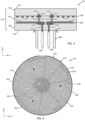
- the ceramic heater 30 comprises a substrate 310 made of ceramic materials, such as aluminum nitride (AIN), a heating layer 330 for generating heat, a routing layer 340, one or more first conductive vias 350, one or more second conductive vias 370, and a substrate shaft 380.
- the first conductive vias 350 are disposed between the heating layer 330 and the routing layer 340 for connecting the heating layer 330 to the routing layer 340, and the second conductive vias 370 are disposed between the routing layer 340 and at least one terminal wire 390.
- the ceramic heater 30 may be used as a part of a support pedestal in semiconductor processing.
- the substrate 310 defines a first surface 312 for heating a target thereon and a second surface 314 from which the at least one terminal wire 390 extends.
- the substrate shaft 380 is bonded to the second surface 314 of the substrate 310 via a bonding layer 382 (e.g., a transient liquid phase binding layer) and surrounds the at least one terminal wire 390.
- the substrate 310 may include a plurality of plate members 322, 324, 326.
- the plurality of plate members 322, 324, 326 each have a flat plate configuration, and while three plate members 322, 324, and 326 are shown in the illustrative example, the substrate 310 may include any number of plate members.
- the average surface roughness of adjacent surfaces between the first and second plate members 322, 324 and between the second and third plate members 324, 326 is less than 5 ⁇ m, for example between 100nm and 5 ⁇ m.
- the heating layer 330 is embedded within the first plate member 322 and/or the second plate member 324. In some forms of the present disclosure, the heating layer 330 is disposed in the first plate member 322 and/or the second plate member 324. That is, the heating layer 330 may be disposed in the first plate member 322, the second plate member 324, or the first plate member 322 and the second plate member 324, while remaining within the scope of the present disclosure.
- the routing layer 340 is embedded within the second plate member 324 and/or the third plate member 326. In some forms, the routing layer 340 may be disposed on or partially in the second plate member 324 and/or the third plate member 326.
- the routing layer 340 may be disposed in the second plate member 324, the third plate member 326, or the second plate member 324 and the third plate member 326, while remaining within the scope of the present disclosure.
- At least one of the first conductive vias 350 within the second plate member 324 between heating layer 330 and the routing layer 340 and/or at least one of the second conductive vias 360 within the third plate member 326 may be a trench (not shown) along a side of second plate member 324 or third plate member 326, respectively.
- at least one of the heating layer 330, the routing layer 340, first conductive vias 350 and second conductive vias 370 are molybdenum or a molybdenum alloy.
- the heating layer 330 includes at least one heating element 332 and the routing layer 340 includes a plurality of routing layer elements 342.
- the heating layer 330 can include a plurality of circular-arranged heating elements 332 and/or a plurality of serpentine-arranged heating elements 332, among others.
- the heating layer 330 can define a plurality of distinct and independently controlled heating zones as discussed in greater detail below.
- the first conductive vias 350 include a fastener 360 that comprise a head 362, a shaft 364, and a cap 366.
- the fasteners 360 extend through the second plate member 324 and in at least one aspect, the head 362, shaft 364, and cap 366 are molybdenum or a molybdenum alloy.
- the second conductive vias 370 may include fasteners (not shown).
- the first conductive vias 350 and/or the second conductive vias 370 may be formed from a rod, pin, shaft, among others, disposed in the second plate member 324 and the third plate member 326, respectively.
- the substrate 310 is manufactured using transient liquid phase bonding as described above with respect to substrate 110.
- trenches and vias (not labeled) are formed in the second plate member 324, and molybdenum layers are deposited in the trenches and removed from outer surfaces of the second plate member 324.
- Silicon layers are deposited onto the molybdenum layers in the trenches and removed from outer surfaces of the second plate member 322, and the conductive vias 360 are inserted through the vias in the second plate member 324.
- Trenches and vias are formed in the third plate member 326, and the plate members 322, 324, 326 are assembled and transient liquid phase bonded together.
- trenches are formed in the substrate shaft 380 and Mo-Si bonding layers are deposited into the trenches such that the substrate shaft 380 is assembled and transient liquid phase bonded to the third plate member before, during or after transient liquid phase bonding of the plate members 322, 324, 326 together.
- FIG. 4 a top view (-z direction) of the ceramic heater 30 according to one form of the present disclosure is shown.
- the first plate member 322 is not shown in FIG. 4 in order to show the heating layer 330 in greater detail.
- the ceramic heater 30 shown in FIG. 4 includes a plurality of molybdenum heating elements 332, a plurality of routing layers 340, and a plurality of conductive vias 350 extending between and electrically connecting the plurality of molybdenum heating elements to the plurality of routing layers 340.
- the ceramic heater 30 shown in FIG. 4 includes six (6) distinct and independently controlled heat zones 334.
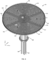
- the ceramic heater 30 shown in FIG. 5 includes a plurality of molybdenum heating elements 332, a plurality of routing layers 340, and a plurality of conductive vias 350 extending between and electrically connecting the plurality of molybdenum heating elements to the plurality of routing layers 340. Also, the ceramic heater 30 shown in FIG. 5 includes six (6) distinct and independently controlled heat zones 336.
- FIG. 6 a perspective view of the ceramic heater in FIG. 5 is shown with the six heat zones 336, substrate shaft 380 and terminal wires 390.
- compositions that can be used to transient liquid phase bond plate members together as described herein include titanium-aluminum layers, palladium-aluminum layers, manganese-aluminum layers, niobium-silicon layers, and tungsten-silicon layers, among others.
- first, second, third, etc. may be used to describe various elements, components, regions, layers and/or sections, these elements, components, regions, layers and/or sections, should not be limited by these terms. These terms may be only used to distinguish one element, component, region, layer and/or section, from another element, component, region, layer and/or section. Terms such as “first,” “second,” and other numerical terms when used herein do not imply a sequence or order unless clearly indicated by the context. Thus, a first element, component, region, layer or section, could be termed a second element, component, region, layer or section without departing from the teachings of the example forms. Furthermore, an element, component, region, layer or section may be termed a "second” element, component, region, layer or section, without the need for an element, component, region, layer or section termed a "first" element, component, region, layer or section.
- Spacially relative terms such as “inner,” “outer,” “beneath,” “below,” “lower,” “above,” “upper,” and the like, may be used herein for ease of description to describe one element or feature's relationship to another element(s) or feature(s) as illustrated in the figures.
- Spatially relative terms may be intended to encompass different orientations of the device in use or operation in addition to the orientation depicted in the figures. For example, if the device in the figures is turned over, elements described as “below” or “beneath” other elements or features would then be oriented “above” the other elements or features.
- the example term “below” can encompass both an orientation of above or below.
- the device may be otherwise oriented (rotated 90 degrees or at other orientations) and the spatially relative descriptors used herein interpreted accordingly.
- the phrase at least one of A, B, and C should be construed to mean a logical (A OR B OR C), using a non-exclusive logical OR, and should not be construed to mean "at least one of A, at least one of B, and at least one of C.
Landscapes
- Engineering & Computer Science (AREA)
- Chemical & Material Sciences (AREA)
- Ceramic Engineering (AREA)
- Manufacturing & Machinery (AREA)
- Inorganic Chemistry (AREA)
- Materials Engineering (AREA)
- Structural Engineering (AREA)
- Organic Chemistry (AREA)
- Resistance Heating (AREA)
- Surface Heating Bodies (AREA)
- Ceramic Products (AREA)
- Laminated Bodies (AREA)
Claims (13)
- Heizvorrichtung (30), umfassend:ein Keramiksubstrat (310); undeine Heizschicht (330), wobei die Heizschicht (330) über eine vorübergehende Flüssigphasenbindung mit dem Keramiksubstrat (310) verbunden ist, gekennzeichnet durchdie Heizvorrichtung, die ferner eine Leitschicht (340) und eine Vielzahl von ersten leitenden Durchkontaktierungen (350) umfasst, die die Heizschicht (330) mit der Leitschicht (340) verbinden,wobei das Keramiksubstrat (310) ein AIN-Substrat ist, die Leitschicht (340) und die Vielzahl von ersten leitenden Durchkontaktierungen (350) aus einem Molybdänmaterial hergestellt sind und die Leitschicht (340) und die Vielzahl von ersten leitenden Durchkontaktierungen (350) über die transiente Flüssigphasenbindung mit dem AIN-Substrat verbunden sind.
- Heizvorrichtung (30) nach Anspruch 1, die ferner eine Vielzahl von zweiten leitenden Durchkontaktierungen (370) umfasst, die die Leitschicht (340) mit einer Oberfläche des AIN-Substrats (310) verbinden.
- Heizvorrichtung (30) nach Anspruch 1, wobei das AIN-Substrat (310) eine Vielzahl von Plattenelementen (322, 324, 326) umfasst, die über eine transiente Flüssigphasenbindung mit dem Molybdänmaterial verbunden sind.
- Heizvorrichtung (30) nach Anspruch 3, wobei die die Vielzahl von Plattenelementen (322, 324, 326) ein erstes Plattenelement (322) und ein zweites Plattenelement (324) enthält, durch die sich die Vielzahl von ersten leitenden Durchkontaktierungen (350) aus dem Molybdänmaterial erstrecken.
- Heizvorrichtung (30) nach Anspruch 4, wobei die Heizschicht (330) in mindestens einen von dem ersten Plattenelement (322) und dem zweiten Plattenelement (324) eingebettet ist.
- Heizvorrichtung (30) nach Anspruch 4, wobei eine durchschnittliche Oberflächenrauheit zwischen dem ersten Plattenelement (322) und dem zweiten Plattenelement (324) weniger als 5 µm beträgt.
- Heizvorrichtung (30) nach Anspruch 4, die ferner eine Leitschicht (340) aus dem Molybdänmaterial umfasst, die in mindestens einen von dem zweiten Plattenelement (324) und ein drittes Plattenelement (326) eingebettet ist und mit der Vielzahl von ersten leitenden Durchkontaktierungen (350) in Kontakt steht.
- Heizvorrichtung (30) nach Anspruch 7, die ferner Anschlussdrähte (390) umfasst, die mit dem Anschluss verbunden sind.
- Heizvorrichtung (30) nach Anspruch 4, die ferner ein Anschlussschichtmaterial umfasst, das in mindestens einen von dem zweiten Plattenelement und dem dritten Plattenelement eingebettet ist.
- Heizvorrichtung (30) nach Anspruch 9, wobei die Anschlussschicht Molybdän und Silizium umfasst.
- Heizvorrichtung (30) nach Anspruch 10, die ferner mindestens einen von einer Molybdän-Silizium(Mo-Si)-Legierung und/oder einem intermetallischen Mo-Si-Material zwischen der Heizschicht (330) und dem AIN-Substrat (310) umfasst.
- Heizvorrichtung (30) nach Anspruch 3, wobei die Vielzahl von Plattenelementen (322, 324, 326) ein erstes Plattenelement (322), ein zweites Plattenelement (324), durch das sich eine Vielzahl von ersten leitenden Durchkontaktierungen (350) aus dem Molybdänmaterial erstrecken, und ein drittes Plattenelement (326) enthält, durch das sich eine Vielzahl von zweiten leitenden Durchkontaktierungen (370) aus dem Molybdänmaterial erstrecken.
- Heizvorrichtung (30) nach Anspruch 12, wobei die Heizschicht (330) in mindestens einen von dem ersten Plattenelement (322) und dem zweiten Plattenelement (324) eingebettet ist.
Applications Claiming Priority (2)
| Application Number | Priority Date | Filing Date | Title |
|---|---|---|---|
| US201962899189P | 2019-09-12 | 2019-09-12 | |
| PCT/US2020/050678 WO2021051062A1 (en) | 2019-09-12 | 2020-09-14 | Ceramic heater and method of forming using transient liquid phase bonding |
Publications (3)
| Publication Number | Publication Date |
|---|---|
| EP4029351A1 EP4029351A1 (de) | 2022-07-20 |
| EP4029351C0 EP4029351C0 (de) | 2024-04-24 |
| EP4029351B1 true EP4029351B1 (de) | 2024-04-24 |
Family
ID=72645007
Family Applications (1)
| Application Number | Title | Priority Date | Filing Date |
|---|---|---|---|
| EP20780535.9A Active EP4029351B1 (de) | 2019-09-12 | 2020-09-14 | Keramisches heizelement und verfahren zur herstellung unter verwendung einer übergangsflüssigkeitsphasenbindung |
Country Status (7)
| Country | Link |
|---|---|
| US (1) | US11943845B2 (de) |
| EP (1) | EP4029351B1 (de) |
| JP (1) | JP7657780B2 (de) |
| KR (1) | KR102921299B1 (de) |
| CN (1) | CN114557125A (de) |
| TW (2) | TWI892052B (de) |
| WO (1) | WO2021051062A1 (de) |
Families Citing this family (4)
| Publication number | Priority date | Publication date | Assignee | Title |
|---|---|---|---|---|
| US11083050B2 (en) * | 2017-11-21 | 2021-08-03 | Watlow Electric Manufacturing Company | Integrated heater and method of manufacture |
| JP7489940B2 (ja) * | 2021-05-11 | 2024-05-24 | 京セラ株式会社 | 試料保持具 |
| JP2024013384A (ja) * | 2022-07-20 | 2024-02-01 | 日本発條株式会社 | ヒータユニット |
| US12469765B2 (en) | 2022-09-22 | 2025-11-11 | Apple Inc. | Thermally enhanced chip-on-wafer or wafer-on-wafer bonding |
Family Cites Families (23)
| Publication number | Priority date | Publication date | Assignee | Title |
|---|---|---|---|---|
| JP4013386B2 (ja) * | 1998-03-02 | 2007-11-28 | 住友電気工業株式会社 | 半導体製造用保持体およびその製造方法 |
| US6511759B1 (en) * | 2000-02-07 | 2003-01-28 | Carl Schalansky | Means and method for producing multi-element laminar structures |
| TW200304909A (en) | 2000-07-04 | 2003-10-16 | Ibiden Co Ltd | Aluminum nitride sintered compact, ceramic substrate, ceramic heater and electrostatic chuck |
| US6565990B2 (en) * | 2001-05-30 | 2003-05-20 | General Electric Company | Bonded niobium silicide and molybdenum silicide composite articles and method of manufacture |
| JP3842695B2 (ja) | 2002-05-27 | 2006-11-08 | 日本碍子株式会社 | 半導体処理装置 |
| JP4483161B2 (ja) | 2002-08-13 | 2010-06-16 | 住友電気工業株式会社 | 窒化アルミニウム焼結体、メタライズ基板、ヒータ、治具および窒化アルミニウム焼結体の製造方法 |
| JP3975944B2 (ja) | 2003-02-27 | 2007-09-12 | 住友電気工業株式会社 | 半導体あるいは液晶製造装置用保持体およびそれを搭載した半導体あるいは液晶製造装置 |
| JP4071204B2 (ja) | 2004-02-27 | 2008-04-02 | Tdk株式会社 | 多層セラミック基板の製造方法 |
| TW200633947A (en) | 2005-02-16 | 2006-10-01 | Ngk Insulators Ltd | Joined body and manufacturing method for the same |
| CN101101855A (zh) * | 2006-07-05 | 2008-01-09 | 通用电气公司 | 电阻加热元件用的电极图案以及衬底处理装置 |
| JP5688203B2 (ja) | 2007-11-01 | 2015-03-25 | 株式会社半導体エネルギー研究所 | 半導体基板の作製方法 |
| JP4986830B2 (ja) | 2007-12-07 | 2012-07-25 | 日本碍子株式会社 | 基板保持体及びその製造方法 |
| JP5821389B2 (ja) * | 2011-04-20 | 2015-11-24 | 三菱マテリアル株式会社 | パワーモジュール用基板の製造方法及びパワーモジュール用基板 |
| WO2013130918A1 (en) * | 2012-02-29 | 2013-09-06 | Harris, Jonathan, H. | Transient liquid phase, pressureless joining of aluminum nitride components |
| US9044822B2 (en) * | 2012-04-17 | 2015-06-02 | Toyota Motor Engineering & Manufacturing North America, Inc. | Transient liquid phase bonding process for double sided power modules |
| FR2999805B1 (fr) * | 2012-12-17 | 2017-12-22 | Commissariat Energie Atomique | Procede de realisation d'un dispositif de detection infrarouge |
| JP6332108B2 (ja) * | 2015-03-30 | 2018-05-30 | 三菱マテリアル株式会社 | ヒートシンク付パワーモジュール用基板の製造方法 |
| JP6690918B2 (ja) * | 2015-10-16 | 2020-04-28 | 日本特殊陶業株式会社 | 加熱部材、静電チャック、及びセラミックヒータ |
| JP7194592B2 (ja) | 2016-04-07 | 2022-12-22 | マテリオン コーポレイション | 酸化ベリリウム一体抵抗加熱器 |
| US11013068B2 (en) | 2016-06-09 | 2021-05-18 | Ngk Spark Plug Co., Ltd. | Multilayer heating body |
| TWI670312B (zh) | 2018-07-24 | 2019-09-01 | 佳勝科技股份有限公司 | 電路板結構以及用於形成絕緣基板的組成物 |
| JP7303820B2 (ja) * | 2017-11-21 | 2023-07-05 | ワトロー エレクトリック マニュファクチュアリング カンパニー | ビアを有さない複数領域ペデスタルヒーター |
| WO2019102794A1 (ja) | 2017-11-24 | 2019-05-31 | トーカロ株式会社 | 発熱部材 |
-
2020
- 2020-09-14 EP EP20780535.9A patent/EP4029351B1/de active Active
- 2020-09-14 JP JP2022516088A patent/JP7657780B2/ja active Active
- 2020-09-14 TW TW111142751A patent/TWI892052B/zh active
- 2020-09-14 US US17/020,063 patent/US11943845B2/en active Active
- 2020-09-14 CN CN202080072020.3A patent/CN114557125A/zh active Pending
- 2020-09-14 WO PCT/US2020/050678 patent/WO2021051062A1/en not_active Ceased
- 2020-09-14 KR KR1020227012036A patent/KR102921299B1/ko active Active
- 2020-09-14 TW TW109131570A patent/TWI785381B/zh active
Also Published As
| Publication number | Publication date |
|---|---|
| JP7657780B2 (ja) | 2025-04-07 |
| EP4029351A1 (de) | 2022-07-20 |
| US20210084719A1 (en) | 2021-03-18 |
| TWI785381B (zh) | 2022-12-01 |
| CN114557125A (zh) | 2022-05-27 |
| KR20220062074A (ko) | 2022-05-13 |
| KR102921299B1 (ko) | 2026-01-30 |
| US11943845B2 (en) | 2024-03-26 |
| TW202113297A (zh) | 2021-04-01 |
| TWI892052B (zh) | 2025-08-01 |
| JP2022548244A (ja) | 2022-11-17 |
| EP4029351C0 (de) | 2024-04-24 |
| TW202326057A (zh) | 2023-07-01 |
| WO2021051062A1 (en) | 2021-03-18 |
Similar Documents
| Publication | Publication Date | Title |
|---|---|---|
| EP4029351B1 (de) | Keramisches heizelement und verfahren zur herstellung unter verwendung einer übergangsflüssigkeitsphasenbindung | |
| US20070169703A1 (en) | Advanced ceramic heater for substrate processing | |
| KR102213060B1 (ko) | 저 열팽창 계수의 정상부를 갖는 받침부 구성 | |
| US6503368B1 (en) | Substrate support having bonded sections and method | |
| US7353979B2 (en) | Method of fabricating substrate placing stage | |
| EP4022672B1 (de) | Thermischer diffusor für einen halbleiterwaferhalter | |
| US20210078092A1 (en) | Ceramic-aluminum assembly with bonding trenches | |
| KR20130099792A (ko) | 이종접합 냉각구조체 및 그 제조방법 | |
| JPH0870036A (ja) | 静電チャック | |
| KR102735500B1 (ko) | 모든 알루미늄 히터 | |
| JP3941542B2 (ja) | セラミックスと金属の気密接合構造及び該構造を有する装置部品 | |
| JPH0967685A (ja) | プラズマエッチング用平行平板電極 | |
| WO2025128940A1 (en) | Molybdenum sputtering target assembly and method of making | |
| JPH08107140A (ja) | 静電チャック |
Legal Events
| Date | Code | Title | Description |
|---|---|---|---|
| STAA | Information on the status of an ep patent application or granted ep patent |
Free format text: STATUS: UNKNOWN |
|
| STAA | Information on the status of an ep patent application or granted ep patent |
Free format text: STATUS: THE INTERNATIONAL PUBLICATION HAS BEEN MADE |
|
| PUAI | Public reference made under article 153(3) epc to a published international application that has entered the european phase |
Free format text: ORIGINAL CODE: 0009012 |
|
| STAA | Information on the status of an ep patent application or granted ep patent |
Free format text: STATUS: REQUEST FOR EXAMINATION WAS MADE |
|
| 17P | Request for examination filed |
Effective date: 20220322 |
|
| AK | Designated contracting states |
Kind code of ref document: A1 Designated state(s): AL AT BE BG CH CY CZ DE DK EE ES FI FR GB GR HR HU IE IS IT LI LT LU LV MC MK MT NL NO PL PT RO RS SE SI SK SM TR |
|
| DAV | Request for validation of the european patent (deleted) | ||
| DAX | Request for extension of the european patent (deleted) | ||
| GRAP | Despatch of communication of intention to grant a patent |
Free format text: ORIGINAL CODE: EPIDOSNIGR1 |
|
| STAA | Information on the status of an ep patent application or granted ep patent |
Free format text: STATUS: GRANT OF PATENT IS INTENDED |
|
| INTG | Intention to grant announced |
Effective date: 20231115 |
|
| GRAS | Grant fee paid |
Free format text: ORIGINAL CODE: EPIDOSNIGR3 |
|
| GRAA | (expected) grant |
Free format text: ORIGINAL CODE: 0009210 |
|
| STAA | Information on the status of an ep patent application or granted ep patent |
Free format text: STATUS: THE PATENT HAS BEEN GRANTED |
|
| AK | Designated contracting states |
Kind code of ref document: B1 Designated state(s): AL AT BE BG CH CY CZ DE DK EE ES FI FR GB GR HR HU IE IS IT LI LT LU LV MC MK MT NL NO PL PT RO RS SE SI SK SM TR |
|
| REG | Reference to a national code |
Ref country code: GB Ref legal event code: FG4D |
|
| REG | Reference to a national code |
Ref country code: CH Ref legal event code: EP |
|
| REG | Reference to a national code |
Ref country code: DE Ref legal event code: R096 Ref document number: 602020029704 Country of ref document: DE |
|
| REG | Reference to a national code |
Ref country code: IE Ref legal event code: FG4D |
|
| U01 | Request for unitary effect filed |
Effective date: 20240523 |
|
| U07 | Unitary effect registered |
Designated state(s): AT BE BG DE DK EE FI FR IT LT LU LV MT NL PT SE SI Effective date: 20240603 |
|
| PG25 | Lapsed in a contracting state [announced via postgrant information from national office to epo] |
Ref country code: IS Free format text: LAPSE BECAUSE OF FAILURE TO SUBMIT A TRANSLATION OF THE DESCRIPTION OR TO PAY THE FEE WITHIN THE PRESCRIBED TIME-LIMIT Effective date: 20240824 |
|
| PG25 | Lapsed in a contracting state [announced via postgrant information from national office to epo] |
Ref country code: HR Free format text: LAPSE BECAUSE OF FAILURE TO SUBMIT A TRANSLATION OF THE DESCRIPTION OR TO PAY THE FEE WITHIN THE PRESCRIBED TIME-LIMIT Effective date: 20240424 |
|
| PG25 | Lapsed in a contracting state [announced via postgrant information from national office to epo] |
Ref country code: GR Free format text: LAPSE BECAUSE OF FAILURE TO SUBMIT A TRANSLATION OF THE DESCRIPTION OR TO PAY THE FEE WITHIN THE PRESCRIBED TIME-LIMIT Effective date: 20240725 |
|
| PG25 | Lapsed in a contracting state [announced via postgrant information from national office to epo] |
Ref country code: ES Free format text: LAPSE BECAUSE OF FAILURE TO SUBMIT A TRANSLATION OF THE DESCRIPTION OR TO PAY THE FEE WITHIN THE PRESCRIBED TIME-LIMIT Effective date: 20240424 |
|
| PG25 | Lapsed in a contracting state [announced via postgrant information from national office to epo] |
Ref country code: PL Free format text: LAPSE BECAUSE OF FAILURE TO SUBMIT A TRANSLATION OF THE DESCRIPTION OR TO PAY THE FEE WITHIN THE PRESCRIBED TIME-LIMIT Effective date: 20240424 |
|
| PG25 | Lapsed in a contracting state [announced via postgrant information from national office to epo] |
Ref country code: PL Free format text: LAPSE BECAUSE OF FAILURE TO SUBMIT A TRANSLATION OF THE DESCRIPTION OR TO PAY THE FEE WITHIN THE PRESCRIBED TIME-LIMIT Effective date: 20240424 Ref country code: NO Free format text: LAPSE BECAUSE OF FAILURE TO SUBMIT A TRANSLATION OF THE DESCRIPTION OR TO PAY THE FEE WITHIN THE PRESCRIBED TIME-LIMIT Effective date: 20240724 Ref country code: IS Free format text: LAPSE BECAUSE OF FAILURE TO SUBMIT A TRANSLATION OF THE DESCRIPTION OR TO PAY THE FEE WITHIN THE PRESCRIBED TIME-LIMIT Effective date: 20240824 Ref country code: HR Free format text: LAPSE BECAUSE OF FAILURE TO SUBMIT A TRANSLATION OF THE DESCRIPTION OR TO PAY THE FEE WITHIN THE PRESCRIBED TIME-LIMIT Effective date: 20240424 Ref country code: GR Free format text: LAPSE BECAUSE OF FAILURE TO SUBMIT A TRANSLATION OF THE DESCRIPTION OR TO PAY THE FEE WITHIN THE PRESCRIBED TIME-LIMIT Effective date: 20240725 Ref country code: ES Free format text: LAPSE BECAUSE OF FAILURE TO SUBMIT A TRANSLATION OF THE DESCRIPTION OR TO PAY THE FEE WITHIN THE PRESCRIBED TIME-LIMIT Effective date: 20240424 Ref country code: RS Free format text: LAPSE BECAUSE OF FAILURE TO SUBMIT A TRANSLATION OF THE DESCRIPTION OR TO PAY THE FEE WITHIN THE PRESCRIBED TIME-LIMIT Effective date: 20240724 |
|
| U20 | Renewal fee for the european patent with unitary effect paid |
Year of fee payment: 5 Effective date: 20240927 |
|
| PG25 | Lapsed in a contracting state [announced via postgrant information from national office to epo] |
Ref country code: CZ Free format text: LAPSE BECAUSE OF FAILURE TO SUBMIT A TRANSLATION OF THE DESCRIPTION OR TO PAY THE FEE WITHIN THE PRESCRIBED TIME-LIMIT Effective date: 20240424 |
|
| PG25 | Lapsed in a contracting state [announced via postgrant information from national office to epo] |
Ref country code: SK Free format text: LAPSE BECAUSE OF FAILURE TO SUBMIT A TRANSLATION OF THE DESCRIPTION OR TO PAY THE FEE WITHIN THE PRESCRIBED TIME-LIMIT Effective date: 20240424 Ref country code: RO Free format text: LAPSE BECAUSE OF FAILURE TO SUBMIT A TRANSLATION OF THE DESCRIPTION OR TO PAY THE FEE WITHIN THE PRESCRIBED TIME-LIMIT Effective date: 20240424 |
|
| REG | Reference to a national code |
Ref country code: DE Ref legal event code: R097 Ref document number: 602020029704 Country of ref document: DE |
|
| PG25 | Lapsed in a contracting state [announced via postgrant information from national office to epo] |
Ref country code: SM Free format text: LAPSE BECAUSE OF FAILURE TO SUBMIT A TRANSLATION OF THE DESCRIPTION OR TO PAY THE FEE WITHIN THE PRESCRIBED TIME-LIMIT Effective date: 20240424 |
|
| PG25 | Lapsed in a contracting state [announced via postgrant information from national office to epo] |
Ref country code: SM Free format text: LAPSE BECAUSE OF FAILURE TO SUBMIT A TRANSLATION OF THE DESCRIPTION OR TO PAY THE FEE WITHIN THE PRESCRIBED TIME-LIMIT Effective date: 20240424 Ref country code: SK Free format text: LAPSE BECAUSE OF FAILURE TO SUBMIT A TRANSLATION OF THE DESCRIPTION OR TO PAY THE FEE WITHIN THE PRESCRIBED TIME-LIMIT Effective date: 20240424 Ref country code: RO Free format text: LAPSE BECAUSE OF FAILURE TO SUBMIT A TRANSLATION OF THE DESCRIPTION OR TO PAY THE FEE WITHIN THE PRESCRIBED TIME-LIMIT Effective date: 20240424 Ref country code: CZ Free format text: LAPSE BECAUSE OF FAILURE TO SUBMIT A TRANSLATION OF THE DESCRIPTION OR TO PAY THE FEE WITHIN THE PRESCRIBED TIME-LIMIT Effective date: 20240424 |
|
| PLBE | No opposition filed within time limit |
Free format text: ORIGINAL CODE: 0009261 |
|
| STAA | Information on the status of an ep patent application or granted ep patent |
Free format text: STATUS: NO OPPOSITION FILED WITHIN TIME LIMIT |
|
| 26N | No opposition filed |
Effective date: 20250127 |
|
| PG25 | Lapsed in a contracting state [announced via postgrant information from national office to epo] |
Ref country code: MC Free format text: LAPSE BECAUSE OF FAILURE TO SUBMIT A TRANSLATION OF THE DESCRIPTION OR TO PAY THE FEE WITHIN THE PRESCRIBED TIME-LIMIT Effective date: 20240424 |
|
| REG | Reference to a national code |
Ref country code: CH Ref legal event code: PL |
|
| GBPC | Gb: european patent ceased through non-payment of renewal fee |
Effective date: 20240914 |
|
| PG25 | Lapsed in a contracting state [announced via postgrant information from national office to epo] |
Ref country code: GB Free format text: LAPSE BECAUSE OF NON-PAYMENT OF DUE FEES Effective date: 20240914 |
|
| PG25 | Lapsed in a contracting state [announced via postgrant information from national office to epo] |
Ref country code: CH Free format text: LAPSE BECAUSE OF NON-PAYMENT OF DUE FEES Effective date: 20240930 |
|
| PG25 | Lapsed in a contracting state [announced via postgrant information from national office to epo] |
Ref country code: IE Free format text: LAPSE BECAUSE OF NON-PAYMENT OF DUE FEES Effective date: 20240914 |
|
| U20 | Renewal fee for the european patent with unitary effect paid |
Year of fee payment: 6 Effective date: 20250929 |
|
| PG25 | Lapsed in a contracting state [announced via postgrant information from national office to epo] |
Ref country code: CY Free format text: LAPSE BECAUSE OF FAILURE TO SUBMIT A TRANSLATION OF THE DESCRIPTION OR TO PAY THE FEE WITHIN THE PRESCRIBED TIME-LIMIT; INVALID AB INITIO Effective date: 20200914 |
|
| PG25 | Lapsed in a contracting state [announced via postgrant information from national office to epo] |
Ref country code: HU Free format text: LAPSE BECAUSE OF FAILURE TO SUBMIT A TRANSLATION OF THE DESCRIPTION OR TO PAY THE FEE WITHIN THE PRESCRIBED TIME-LIMIT; INVALID AB INITIO Effective date: 20200914 |