EP4030430A2 - Erzeugung von referenzwerten für stt-mram zur erfassung des mittelpunkts - Google Patents
Erzeugung von referenzwerten für stt-mram zur erfassung des mittelpunkts Download PDFInfo
- Publication number
- EP4030430A2 EP4030430A2 EP21210921.9A EP21210921A EP4030430A2 EP 4030430 A2 EP4030430 A2 EP 4030430A2 EP 21210921 A EP21210921 A EP 21210921A EP 4030430 A2 EP4030430 A2 EP 4030430A2
- Authority
- EP
- European Patent Office
- Prior art keywords
- bit line
- magnetoresistive
- magnetoresistive device
- column
- bit
- Prior art date
- Legal status (The legal status is an assumption and is not a legal conclusion. Google has not performed a legal analysis and makes no representation as to the accuracy of the status listed.)
- Pending
Links
Images



Classifications
-
- G—PHYSICS
- G11—INFORMATION STORAGE
- G11C—STATIC STORES
- G11C11/00—Digital stores characterised by the use of particular electric or magnetic storage elements; Storage elements therefor
- G11C11/02—Digital stores characterised by the use of particular electric or magnetic storage elements; Storage elements therefor using magnetic elements
- G11C11/16—Digital stores characterised by the use of particular electric or magnetic storage elements; Storage elements therefor using magnetic elements using elements in which the storage effect is based on magnetic spin effect
- G11C11/165—Auxiliary circuits
- G11C11/1673—Reading or sensing circuits or methods
-
- G—PHYSICS
- G11—INFORMATION STORAGE
- G11C—STATIC STORES
- G11C11/00—Digital stores characterised by the use of particular electric or magnetic storage elements; Storage elements therefor
- G11C11/02—Digital stores characterised by the use of particular electric or magnetic storage elements; Storage elements therefor using magnetic elements
- G11C11/16—Digital stores characterised by the use of particular electric or magnetic storage elements; Storage elements therefor using magnetic elements using elements in which the storage effect is based on magnetic spin effect
- G11C11/165—Auxiliary circuits
- G11C11/1653—Address circuits or decoders
- G11C11/1655—Bit-line or column circuits
-
- G—PHYSICS
- G11—INFORMATION STORAGE
- G11C—STATIC STORES
- G11C11/00—Digital stores characterised by the use of particular electric or magnetic storage elements; Storage elements therefor
- G11C11/02—Digital stores characterised by the use of particular electric or magnetic storage elements; Storage elements therefor using magnetic elements
- G11C11/16—Digital stores characterised by the use of particular electric or magnetic storage elements; Storage elements therefor using magnetic elements using elements in which the storage effect is based on magnetic spin effect
- G11C11/165—Auxiliary circuits
- G11C11/1659—Cell access
-
- G—PHYSICS
- G11—INFORMATION STORAGE
- G11C—STATIC STORES
- G11C29/00—Checking stores for correct operation ; Subsequent repair; Testing stores during standby or offline operation
- G11C29/02—Detection or location of defective auxiliary circuits, e.g. defective refresh counters
-
- G—PHYSICS
- G11—INFORMATION STORAGE
- G11C—STATIC STORES
- G11C29/00—Checking stores for correct operation ; Subsequent repair; Testing stores during standby or offline operation
- G11C29/02—Detection or location of defective auxiliary circuits, e.g. defective refresh counters
- G11C29/021—Detection or location of defective auxiliary circuits, e.g. defective refresh counters in voltage or current generators
-
- G—PHYSICS
- G11—INFORMATION STORAGE
- G11C—STATIC STORES
- G11C29/00—Checking stores for correct operation ; Subsequent repair; Testing stores during standby or offline operation
- G11C29/02—Detection or location of defective auxiliary circuits, e.g. defective refresh counters
- G11C29/028—Detection or location of defective auxiliary circuits, e.g. defective refresh counters with adaption or trimming of parameters
-
- G—PHYSICS
- G11—INFORMATION STORAGE
- G11C—STATIC STORES
- G11C29/00—Checking stores for correct operation ; Subsequent repair; Testing stores during standby or offline operation
- G11C29/04—Detection or location of defective memory elements, e.g. cell constructio details, timing of test signals
- G11C29/08—Functional testing, e.g. testing during refresh, power-on self testing [POST] or distributed testing
- G11C29/12—Built-in arrangements for testing, e.g. built-in self testing [BIST] or interconnection details
- G11C29/12005—Built-in arrangements for testing, e.g. built-in self testing [BIST] or interconnection details comprising voltage or current generators
-
- G—PHYSICS
- G11—INFORMATION STORAGE
- G11C—STATIC STORES
- G11C29/00—Checking stores for correct operation ; Subsequent repair; Testing stores during standby or offline operation
- G11C29/04—Detection or location of defective memory elements, e.g. cell constructio details, timing of test signals
- G11C29/08—Functional testing, e.g. testing during refresh, power-on self testing [POST] or distributed testing
- G11C29/12—Built-in arrangements for testing, e.g. built-in self testing [BIST] or interconnection details
- G11C29/18—Address generation devices; Devices for accessing memories, e.g. details of addressing circuits
- G11C29/24—Accessing extra cells, e.g. dummy cells or redundant cells
-
- G—PHYSICS
- G11—INFORMATION STORAGE
- G11C—STATIC STORES
- G11C7/00—Arrangements for writing information into, or reading information out from, a digital store
- G11C7/04—Arrangements for writing information into, or reading information out from, a digital store with means for avoiding disturbances due to temperature effects
-
- G—PHYSICS
- G11—INFORMATION STORAGE
- G11C—STATIC STORES
- G11C7/00—Arrangements for writing information into, or reading information out from, a digital store
- G11C7/14—Dummy cell management; Sense reference voltage generators
-
- G—PHYSICS
- G11—INFORMATION STORAGE
- G11C—STATIC STORES
- G11C11/00—Digital stores characterised by the use of particular electric or magnetic storage elements; Storage elements therefor
- G11C11/02—Digital stores characterised by the use of particular electric or magnetic storage elements; Storage elements therefor using magnetic elements
- G11C11/16—Digital stores characterised by the use of particular electric or magnetic storage elements; Storage elements therefor using magnetic elements using elements in which the storage effect is based on magnetic spin effect
- G11C11/165—Auxiliary circuits
- G11C11/1653—Address circuits or decoders
- G11C11/1657—Word-line or row circuits
-
- G—PHYSICS
- G11—INFORMATION STORAGE
- G11C—STATIC STORES
- G11C29/00—Checking stores for correct operation ; Subsequent repair; Testing stores during standby or offline operation
- G11C29/04—Detection or location of defective memory elements, e.g. cell constructio details, timing of test signals
- G11C29/08—Functional testing, e.g. testing during refresh, power-on self testing [POST] or distributed testing
- G11C29/12—Built-in arrangements for testing, e.g. built-in self testing [BIST] or interconnection details
- G11C2029/1204—Bit line control
Definitions
- Embodiments of the present disclosure relate to magnetoresistive devices. More specifically, embodiments of the present disclosure relate to circuits and methods for midpoint sensing reference generation in spin transfer torque magnetoresistive memory.
- a memory system may include a memory device for storing data and a host (or controller) for controlling operations of the memory device.
- memory devices may be classified into volatile memory (such as, e.g., dynamic random-access memory (DRAM), static random-access memory (SRAM), etc.) and non-volatile memory (such as, e.g., electrically erasable programmable read-only memory (EEPROM), ferroelectric random-access memory (FRAM), phase-change memory (PRAM), magnetoresistive memory (MRAM), resistive random-access memory (RRAM/ReRAM), flash memory, etc.).
- volatile memory such as, e.g., dynamic random-access memory (DRAM), static random-access memory (SRAM), etc.
- non-volatile memory such as, e.g., electrically erasable programmable read-only memory (EEPROM), ferroelectric random-access memory (FRAM), phase-change memory (PRAM), magnetoresistive memory (MRAM), resistive random-access memory (R
- a magnetoresistive stack or a magnetic tunnel junction (MTJ) used in MRAM includes at least one non-magnetic layer (for example, at least one dielectric layer or a non-magnetic yet electrically conductive layer) disposed between a "fixed" magnetic region and a "free” magnetic region, each including one or more layers of ferromagnetic materials.
- Information is stored in the magnetoresistive memory stack by switching, programming, and/or controlling the direction of magnetization vectors in the magnetic layer(s) of the free magnetic region.
- the direction of the magnetization vectors of the free magnetic region may be switched and/or programmed (for example, through spin orbit torque (SOT) and/or spin transfer torque (STT)) by application of a write signal (e.g., one or more current pulses) adjacent to, or through, the magnetoresistive memory stack.
- SOT spin orbit torque
- STT spin transfer torque
- an STT-MRAM device stores information by controlling the resistance across an MTJ such that a read current through the MTJ results in a voltage drop having a magnitude that is based on the state of the magnetoresistive stack.
- the resistance in each MTJ can be varied based on the relative magnetic states of the magnetoresistive layers within the magnetoresistive stack.
- first,” “second,” and the like, herein do not denote any order, quantity, or importance, but rather are used to distinguish one element from another.
- terms of relative orientation, such as “top,” “bottom,” etc. are used with reference to the orientation of the structure illustrated in the figures being described.
- the present disclosure is directed to techniques and implementations for midpoint sensing reference generation in STT-MRAM devices.
- MRAM devices the inventions may be implemented in other memory devices including, but not limited to, EEPROM, FRAM, PRAM, RRAM/ReRAM and/or flash memory.
- Writing to magnetic memory cells can be accomplished by sending a spin-polarized write current through the memory cell where the angular momentum carried by the spin-polarized current can change the magnetic state of the free portion of the magnetic tunnel junction.
- a spin-polarized write current can either be directly driven through the memory cell or can be the result of applying one or more voltages, where the applied voltages result in the desired current.
- the resulting magnetization of the free portion will either be parallel or antiparallel to the fixed portion. If the parallel orientation represents a logic "0", the antiparallel orientation represents a logic "1", or vice versa.
- the direction of write current flow through the memory cell determines whether the memory cell is written to a first state or a second state.
- the magnitude of the write current is typically greater than the magnitude of a read current used to sense the information stored in the memory cells.
- Each memory cell typically includes a magnetic tunnel junction coupled in series with a corresponding selection transistor that allows each memory cell to be individually selected for access.
- each memory cell is coupled between two common lines, which are often referred to as a bit line and a source line.
- a memory array typically includes many bit lines and source lines that allow selective access to subsets of the memory cells within the array.
- Word lines are coupled to the gates of the selection transistors, thereby controlling current flow through the series circuit of each memory cell based on the voltages applied to the ends of the magnetic memory cell by, for example, the bit lines and source lines.
- Midpoint sensing with a toggle MRAM uses a parallel connection of high-state and low-state MTJs (i.e., the components designated as Rhi and Rio in FIG. 1 ) in a sense amplifier.
- a current may be measured for the high-state MTJ and the low-state MTJ, and the sum of the currents for the high-state MTJ and the low-state MTJ may be divided by two to determine a midpoint sensing reference.
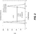
- FIG. 2 depicts an exemplary graph illustrating a resistance distribution for a toggle MRAM device.
- the graph plots resistances of the low-state and high-state MTJs (or bits) against a corresponding number of MTJs.
- Midpoint sensing generally uses a reference, which can be identified in the graph.
- the reference may be at the midpoint between the distribution of low-state MTJs and the distribution of high-state MTJs.
- Magnetoresistance Ratio (MR) may refer to a percentage increase in resistance from a low resistance state to a high resistance state.
- the reference in between the distributions may be obtained using the circuitry (i.e., midpoint generator) illustrated in FIG. 1 .
- FIG. 3 depicts an exemplary diagram illustrating an array structure of a toggle MRAM device.
- the bit cell array 303 includes bit lines 304 and word lines 305.
- the sense amplifiers 301 are connected to the plurality of bit lines 304 to provide appropriate voltages to certain bit lines 304 used to perform an operation (e.g., write, read, etc.).
- Word line drivers 302 generate appropriate word line voltages for word lines 305, in order to select/activate one or more word lines 305 to access MTJ(s) along the selected word line(s) 305.
- the bit cell array 303 includes a plurality of columns (e.g., one or more sets of 32 or 64 columns), with each column including a plurality of MTJs each coupled to a corresponding select transistor and a bit line 304.
- the bit cell array 303 also includes a plurality of rows (e.g., one or more sets of 256 rows), each including a corresponding word line 305.
- An additional reference row for midpoint sensing may be added for every predetermined number of regular rows (e.g., one reference row for every 256 regular rows), such that each reference row is not positioned too far away from the bit cells.
- an additional reference bit line may be added for every predetermined number of regular bit lines 304 (e.g., one reference bit line for every 32 or 64 regular bit lines 304), such that each reference bit line is positioned not too far away from the bit cells.
- the arrangement of the reference rows and the reference bit lines illustrated in FIG. 3 may be applicable to a toggle MRAM device without any significant degradation in performance because, once the reference is set to be high and low, those states are maintained unless there is an interference from an external magnetic field. Such arrangement may not be feasible in, for example, STT-MRAM devices due to various performance reasons, which will be explained in greater detail below.
- FIG. 4 illustrates an exemplary schematic diagram illustrating a local source line array architecture of an STT-MRAM device.
- the STT-MRAM device may include a column multiplexer, comprising a bit line multiplexer 401 and a source line multiplexer 405.
- the bit line multiplexer 401 may be configured to receive a bit line voltage (Vbl) that is generally high.
- the source line multiplexer 405 may be configured to receive a source line voltage (Vsl) of approximately 0 volts or a ground voltage, which may be provided by a ground switch 406. Voltage is applied to the word line 408 that corresponds to the row including the target MTJ 402.
- Each magnetic bit cell may include an MTJ 402 and a select transistor 403 coupled thereto.
- a local source line 404 may be shared across the row of bit cells (e.g., 32 bit cells), the select transistor 403 of each bit cell situated on the same row being coupled to the shared local source line 404.
- the current path for a Write 0 or low state (e.g., down write direction) operation is shown in FIG. 4 , which illustrates that the current travels from the bit line multiplexer 401 toward a MTJ 402 selected using the column multiplexer.
- FIG. 4 illustrates a local source line architecture using a single word line 408.
- Array of magnetic bit cells may include a plurality of word lines, an example of which is illustrated in FIG. 5 .
- FIG. 5 illustrates another exemplary schematic diagram illustrating a local source line array architecture of an STT-MRAM device.
- the array structure 500 of an STT-MRAM device may include a plurality of columns 501 and a plurality of rows 502, with each column including a plurality of magnetic bit cells.
- Each magnetic bit cell may include a select transistor 503 and an MTJ 504.
- Each MTJ may be coupled between a bit line and a first electrode (e.g., a source) of a select transistor, while a second electrode (e.g., a drain) of each select transistor may be coupled to a local source line 505 that runs horizontally across the row in which the MTJ is positioned.
- the local source line may thus be shared across all or a certain number (e.g. 32 bit cells) MTJs positioned in that row.
- a control electrode (e.g., a gate) of each select transistor may be coupled to a word line driver configured to apply voltage to a selected word line or row.
- Each row may contain a single word line 506 that connects to the control electrodes (e.g., gates) of all select transistors positioned across that row.
- the local source line may be a lower level metal layer, and the local source line may be shared among a group of select transistors (e.g., 32 select transistors) situated on the same row.
- select transistors e.g., 32 select transistors
- current travels down the bit line to the active row 507 (i.e., the row selected by the word line driver and to which word line voltage is applied), travels through the corresponding local source line, and travels back up through neighboring bit cells via the respective bit lines, as indicated by the arrows 508 in FIG. 5 .
- the read is performed in a downward direction on a bit line, and the local source line provides for a return path up the other bit lines.
- the bit lines may be on a high level metal layer (e.g., Metal 4) with low resistance.
- the return path includes MTJ devices
- a reference column and a corresponding reference row are added to the array according to FIG. 3 array structure of a toggle MRAM device, and the reference column does not have the same MTJ devices as the other columns, a systematic offset may be introduced.
- the states of MTJs in the return path may cause a mismatch with the reference column during midpoint sensing.
- the reference MTJs for midpoint sensing should be placed near the MTJ that is being read.
- the reference high and low-state MTJs may lose state due to data retention and a read voltage disturbance.
- a poly resistor may be used for a reference, a poly resistor may be too large to fit in a bit cell array, such as the array shown in FIG. 5 . Further, placing the poly resistor outside the bit cell array may not track the word line position for bit line resistance and regular bit line leakage. Additionally, poly resistors may not have voltage and current characteristics identical to those of a regular MTJ. For example, a poly resistor may not track the resistance and MR temperature coefficient of a regular MTJ. Furthermore, a poly resistor may not provide any way to cancel return path MTJ resistance in a local source line array. An exemplary embodiment illustrated in FIG. 6 may minimize or alleviate one or more of the above problems associated with adding a reference region and/or using poly resistors for midpoint reference generation in STT-MRAM devices.
- FIG. 6 depicts an exemplary schematic diagram illustrating a local source line array architecture of an STT-MRAM device configured for midpoint sensing, according to an aspect of the present disclosure.
- An STT-MRAM bit cell array 620 i.e., the bit lines of the array 620
- a plurality of bit lines in the array 620 including the selected bit line 606 and return bit lines 607, may be connected to an input 604 of the sense amplifier 612 through the column selection circuitry 608.
- a reference bit line 605 in the array 620 may be connected to an input 602 of the sense amplifier 612 through the column selection circuitry 608 and a tracking circuitry 610.
- the bit cell array 620 may include a plurality of columns, with each column including a plurality of MTJs 618 and select transistors 617 coupled thereto. Notably, the plurality of columns include a reference column 611 configured for midpoint reference generation.
- the bit cell array 620 may also include a plurality of rows, with each row including a local source line 614 and a plurality of MTJs 618 connected to the local source line 614 via the respective select transistors 617.
- the local source lines 614 may be extended into the reference column 611 and may be connected to the respective second electrodes of the select transistors 617. For example, for every predetermined number of columns (e.g., 32 columns), a reference column 611, including a reference bit line 605 and MTJs 618 connected to the reference bit line 605, may be added as an additional column (e.g., a 33 rd column).
- An advantage of placing a reference bit cell on a same local source line as the other MTJ devices positioned on the same row is that the return path has the same MTJ devices, thus improving uniformity. Additionally, the return path MTJ resistance is present in both reference and regular bit lines during sensing.
- the reference column 611 may include an element 613 connected across the MTJs 618 in the reference column 611.
- the element 613 may be a bridge element (e.g., M3 bridge).
- the bridge element 613 may be formed at the 3 rd metal layer of the STT-MRAM device.
- any metal layer may be used for the bridge element 613.
- any conductive layer may be used for the bridge element 613.
- the STT-MRAM device may use the MTJs 618 in the reference column 611 without having any significant impact from the resistance of the MTJs.
- the MTJs 618 in the reference column 611 does not need to set or reset to high or low states.
- the shared local source line 614 in the reference column 611 enables the same return path for the reference column 611.
- the reference column 611 may include a plurality of shorted MTJ devices, in lieu of using a bridge element. According to yet another exemplary embodiment, the reference column 611 may not include any MTJs and there may be a short connecting the reference bit line 605 directly to select transistors 617 in the reference bit line 605. According to yet another exemplary embodiment, the array 620 may include a plurality of reference bit lines 605 with the bridge elements 613, to reduce the return path MTJ resistance even further.
- the STT-MRAM device may also include circuit elements for adjusting a temperature coefficient of the current on the reference bit line 605.
- the column selection circuitry 608 connected to the reference bit line 605 may in turn be connected to a circuit element 603 within the tracking circuitry 610.
- the circuit element 603 may comprise one or more poly resistors (e.g., a chain of poly resistors with trim capabilities in multiple ways, by shorting to a transfer gate or any other means). Although the poly resistor is outside the bit cell array 620, array word line position impact and bit line leakage may be matched based on the use of the reference column 611. Poly resistors may have different characteristics than an MRAM MTJ.
- a current trim circuitry may be used that has a temperature dependent magnitude of the current that it takes out from the reference bit line 605.
- the current being taken out e.g., current 609
- the amount of resistance the sense amplifier 612 sees on the reference bit line 605 may be controlled.
- poly resistors may have characteristics that are different from those of an MTJ
- the reference current, Iref e.g., circuit element 601
- the reference current, Iref has a temperature coefficient to match the resistance of the parallel high and low-state MTJs across temperature.
- a poly resistor resistance value can be determined by using any one of multiple methods, such as an average of low state MTJ and high state MTJ resistances or parallel resistance configuration of low and high state MTJ resistances with any offset resistance.
- a poly resistor can be implemented with a series of small resistors with a small resolution (e.g., 250 or 500 Ohm) covering a wide range (e.g., 2k Ohm) around a center value (e.g., 4k Ohm).
- the tracking circuitry 610 may use any type of resistor.
- an n-well resistor may be used.
- the resistor trim may be implemented in any one of several ways.
- the resistor trim may be implemented using a transfer gate, and/or a PMOS switch or NMOS switch.
- a PMOS mirror may be used to inject current.
- the tracking circuitry 610 may not contain any current mirror but perform the tracking function by providing a temperature dependent voltage.
- a combination of one or more poly resistors and one or more n-well resistors may be used to adjust a temperature coefficient without adjusting a current.
- trimmable resistors with different temperature coefficients can be configured/programed to achieve a desired temperature coefficient. Further, any two resistive materials with different temperature coefficients may be used together in order to achieve a desired temperature coefficient.
- a switch capacitor may be used in place of the poly resistor.
- the switch capacitor circuit may control a frequency.
- a voltage-controlled oscillator may be used to track temperature in several ways.
- FIG. 7 depicts an exemplary graph illustrating a shift in resistance of a low-state MTJ and a high-state MTJ based on temperature.
- the two curves 701 illustrate resistance distributions of a low-state MTJ and the two curves 702 illustrate resistance distributions of a high-state MTJ.
- the dashed lines illustrate resistance distributions of MTJs at a cold temperature or room temperature.
- the solid lines illustrate resistance distributions of MTJs at a hot temperature.
- Line 703 i.e., midpoint 703 illustrates a midpoint between the solid lines representative of the resistance distributions at the hot temperature.
- Line 704 (i.e., midpoint 704) illustrates a midpoint between the dotted lines representative of the resistance distributions at the cold temperature or room temperature.
- the solid curve for the hot temperature does not drift as far away from the dotted curve for the cold temperature as compared to the high-state distribution represented by the curves 702. In some cases of the low-state distribution represented by the curves 701, the solid curve for the hot temperature may not drift any significant amount from the dotted curve for the cold temperature.
- the midpoint 703 is shifted farther away from the midpoint 704. This may affect the operation of the MRAM device by slowing sensing and/or increasing bit failures.
- the temperature control coefficient may be controlled to protect against the shifting of the high-state distribution.
- the temperature effect may be adjusted.
- the midpoint reference position is adjusted with temperature to maximize the read signal for reading low-state and high-state distributions by the sense amplifier.
- the reference current, Iref may be used to control the temperature coefficient.
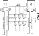
- FIG. 8 depicts an exemplary diagram illustrating a memory architecture of an STT-MRAM device, in accordance with an exemplary embodiment.
- the memory architecture of the STT-MRAM device may include word line drivers, column circuit controls (i.e., gap circuits), read/write circuits comprising sense amplifiers and write drivers, and column multiplexer switches.
- Word line drivers may generate appropriate word line voltages for word lines, in order to select/activate one or more word lines to access MTJ(s) along the selected word line(s).
- Gap circuit may generate and send address signals (e.g., column decode line signals, read/write enable signals, etc.) to column multiplexer switches and read/write circuits (e.g., sense amplifiers and write drivers) to, for example, allow for local decoding that determines which bit lines and source lines are to be driven for a particular operation (e.g., read, write, etc.).
- the local decoding may control the selective driving of the bit lines and source lines by the read/write circuits and may also control the sense amplifiers' selective coupling to, or sensing of, the memory cells for determination of data bits stored therein.
- the read/write enable signals may each provide an indication as to whether memory cells included in the array are to be accessed for a particular operation (e.g., read, write, etc.).
- the column decode line signals may control the column multiplexer switches to select desired bit line and source line columns.
- the column multiplexer switches may comprise bit line column multiplexer switches and source line column multiplexer switches.
- the bit line column multiplexer switches may be configured to provide a unidirectional read current and may be implemented with either a NMOS or a PMOS-type transistor.
- the bit line column multiplexer switches may be further configured to provide a bidirectional write current and may be implemented with a transfer gate, PMOS-type transistor, or auto-booted NMOS transistor.
- the source line column multiplexer switches may be configured to provide a bidirectional current and may be implemented with a transfer gate or auto-booted NMOS transistor. In another embodiment, the source line column multiplexer switches may be connected to bit lines in the bit cell array where a local source line bit cell array is used as depicted in FIG. 5 .
- read/write circuit may comprise sense amplifiers and write drivers, and may be coupled to bit lines and source lines, to provide appropriate voltages to certain bit lines and source lines used to perform an operation.
- the selection of the bit lines and the source lines that are driven is based on the address information received from the gap circuit, where the address information may be decoded and used to determine the memory cells to be accessed. If, for example, a target memory cell is included in a page to be accessed, the read/write circuit may use the decoded address to selectively drive those bit lines and source lines suitable for accessing the corresponding MTJ.
- Reading the state of an MTJ and determining the bit represented by that state may be performed by the read/write circuit, which may include a sense amplifier configured to sense a low voltage signal representing the stored bit and amplify it to a recognizable logic level. Further, reading the states of two MTJs and determining the bit represented by those states (i.e., a differential bit read operation) may also be performed by the read/write circuit including the sense amplifier, the sense amplifier being configured to sense the low power signals representing the states of the MTJs and determine the single bit represented by the differing states.
- a sense amplifier may be connected to each column of MTJs for reading the data values stored therein.
- a sense amplifier may include a preamplifier and a latch, and the preamplifier may regulate voltage on a bit line during a read operation.
- a magnetoresistive device may include an array comprising a plurality of magnetoresistive devices arranged in a plurality of rows and a plurality of columns, wherein each of the plurality of columns comprises a bit line, the bit line being one of a regular bit line and a reference bit line, wherein each magnetoresistive device of the plurality of magnetoresistive devices is coupled to a bit line and a select device, and wherein the plurality of columns comprise a reference column, the reference column comprising a subset of magnetoresistive devices of the plurality of magnetoresistive devices, each of the subset of magnetoresistive devices being coupled between the reference bit line and a bridge element.
- the magnetoresistive device may include wherein the bridge element provides an electrical short across the first set of magnetoresistive devices in the reference column; further comprising a column selection circuitry configured to select a bit line from the plurality of bit line; further comprising a sense amplifier coupled to the column selection circuitry; further comprising a sense amplifier coupled to the column selection circuitry, the sense amplifier including a first input associated with a plurality of regular bit lines and a second input associated with the reference bit line; further comprising a tracking circuitry connected to the reference bit line, the tracking circuitry being configured to adjust a temperature coefficient based on a reference current associated with the reference bit line; wherein the tracking circuitry includes a current mirror to adjust the temperature coefficient; wherein the tracking circuitry includes an NMOS mirror to adjust the temperature coefficient; wherein the tracking circuitry includes a PMOS mirror to adjust the temperature coefficient; wherein the tracking circuitry includes one or more poly resistors configured for resistance trimming; wherein the magnetoresistive devices in each row of the plurality of rows, including a
- a magnetoresistive device may include an array comprising a plurality of memory cells arranged in a plurality of rows and a plurality of columns, each memory cell comprising a magnetic tunnel junction (MTJ), each row comprising a word line, and each column comprising a bit line; a column select device configured to select a bit line from the plurality of bit lines; and a sense amplifier comprising a first input corresponding to a selected bit line, a second input corresponding to a reference bit line, and a data output; and a tracking circuitry connected to the first input to the sense amplifier, the tracking circuitry configured to adjust a temperature coefficient based on a reference current associated with the reference bit line, wherein the plurality of columns comprise a reference column, the reference column comprising a conductive element that provides an electrical short across the MTJs in the reference column.
- MTJ magnetic tunnel junction
- the magnetoresistive device may include wherein the tracking circuitry comprises a current mirror to adjust the temperature coefficient; wherein the tracking circuitry comprises a poly resistor with trim connected to the first input to the sense amplifier; wherein the tracking circuitry comprises a temperature coefficient current to compensate for a temperature effect and a poly resistor with trim connected to the first input to the sense amplifier; further comprising a second reference bit line adjacent to the reference bit line; wherein the conductive element is a bridge element; wherein the bridge element is a metal bridge element.
Landscapes
- Engineering & Computer Science (AREA)
- Computer Hardware Design (AREA)
- Mram Or Spin Memory Techniques (AREA)
- Hall/Mr Elements (AREA)
Applications Claiming Priority (1)
| Application Number | Priority Date | Filing Date | Title |
|---|---|---|---|
| US17/113,595 US11651807B2 (en) | 2020-12-07 | 2020-12-07 | Midpoint sensing reference generation for STT-MRAM |
Publications (2)
| Publication Number | Publication Date |
|---|---|
| EP4030430A2 true EP4030430A2 (de) | 2022-07-20 |
| EP4030430A3 EP4030430A3 (de) | 2022-10-19 |
Family
ID=78819289
Family Applications (1)
| Application Number | Title | Priority Date | Filing Date |
|---|---|---|---|
| EP21210921.9A Pending EP4030430A3 (de) | 2020-12-07 | 2021-11-29 | Erzeugung von referenzwerten für stt-mram zur erfassung des mittelpunkts |
Country Status (3)
| Country | Link |
|---|---|
| US (3) | US11651807B2 (de) |
| EP (1) | EP4030430A3 (de) |
| TW (2) | TWI894404B (de) |
Families Citing this family (2)
| Publication number | Priority date | Publication date | Assignee | Title |
|---|---|---|---|---|
| US11940831B2 (en) * | 2021-12-07 | 2024-03-26 | Infineon Technologies LLC | Current generator for memory sensing |
| CN116978419A (zh) * | 2022-04-21 | 2023-10-31 | 联华电子股份有限公司 | 具温度补偿的感测放大器电路 |
Family Cites Families (13)
| Publication number | Priority date | Publication date | Assignee | Title |
|---|---|---|---|---|
| US6331943B1 (en) * | 2000-08-28 | 2001-12-18 | Motorola, Inc. | MTJ MRAM series-parallel architecture |
| JP3920565B2 (ja) * | 2000-12-26 | 2007-05-30 | 株式会社東芝 | 磁気ランダムアクセスメモリ |
| US6445612B1 (en) * | 2001-08-27 | 2002-09-03 | Motorola, Inc. | MRAM with midpoint generator reference and method for readout |
| JP4084089B2 (ja) * | 2002-05-30 | 2008-04-30 | 株式会社ルネサステクノロジ | 薄膜磁性体記憶装置 |
| US6885600B2 (en) * | 2002-09-10 | 2005-04-26 | Silicon Storage Technology, Inc. | Differential sense amplifier for multilevel non-volatile memory |
| TWI223259B (en) * | 2003-01-07 | 2004-11-01 | Ind Tech Res Inst | A reference mid-point current generator for a magnetic random access memory |
| US7057958B2 (en) * | 2003-09-30 | 2006-06-06 | Sandisk Corporation | Method and system for temperature compensation for memory cells with temperature-dependent behavior |
| KR100528341B1 (ko) * | 2003-12-30 | 2005-11-15 | 삼성전자주식회사 | 자기 램 및 그 읽기방법 |
| US8902641B2 (en) * | 2012-04-10 | 2014-12-02 | Taiwan Semiconductor Manufacturing Co., Ltd. | Adjusting reference resistances in determining MRAM resistance states |
| US9741434B2 (en) * | 2013-03-22 | 2017-08-22 | SK Hynix Inc. | Resistance change memory |
| US8947920B2 (en) * | 2013-03-22 | 2015-02-03 | Masahiro Takahashi | Memory device |
| KR102476355B1 (ko) * | 2018-05-10 | 2022-12-09 | 삼성전자주식회사 | 레퍼런스 셀을 포함하는 저항성 메모리 장치 및 그것의 동작 방법 |
| US10699763B2 (en) * | 2018-05-18 | 2020-06-30 | Marvell International Ltd. | Merged write driver based on local source line MRAM architecture |
-
2020
- 2020-12-07 US US17/113,595 patent/US11651807B2/en active Active
-
2021
- 2021-11-29 EP EP21210921.9A patent/EP4030430A3/de active Pending
- 2021-12-03 TW TW110145171A patent/TWI894404B/zh active
- 2021-12-03 TW TW114129710A patent/TW202548747A/zh unknown
-
2023
- 2023-04-10 US US18/297,793 patent/US12165684B2/en active Active
-
2024
- 2024-11-01 US US18/934,463 patent/US20250061933A1/en active Pending
Also Published As
| Publication number | Publication date |
|---|---|
| US11651807B2 (en) | 2023-05-16 |
| US20230245692A1 (en) | 2023-08-03 |
| US12165684B2 (en) | 2024-12-10 |
| US20250061933A1 (en) | 2025-02-20 |
| TW202548747A (zh) | 2025-12-16 |
| TWI894404B (zh) | 2025-08-21 |
| EP4030430A3 (de) | 2022-10-19 |
| TW202240578A (zh) | 2022-10-16 |
| US20220180913A1 (en) | 2022-06-09 |
Similar Documents
| Publication | Publication Date | Title |
|---|---|---|
| US6868025B2 (en) | Temperature compensated RRAM circuit | |
| KR101266600B1 (ko) | 저항성 메모리 | |
| US7187577B1 (en) | Method and system for providing current balanced writing for memory cells and magnetic devices | |
| US8014219B2 (en) | Semiconductor memory device | |
| US20250061933A1 (en) | Midpoint sensing reference generation for stt-mram | |
| US8040718B2 (en) | Semiconductor memory device | |
| US10269404B2 (en) | Resistance change memory | |
| US8036015B2 (en) | Resistive memory | |
| US7196957B2 (en) | Magnetic memory structure using heater lines to assist in writing operations | |
| US10892000B2 (en) | Semiconductor memory device | |
| CN113129953B (zh) | 磁性随机存储器的读电路 | |
| TW202307835A (zh) | 用於窄範圍感測放大器的參考生成 | |
| US7505348B2 (en) | Balanced and bi-directional bit line paths for memory arrays with programmable memory cells | |
| JP2011023046A (ja) | 抵抗変化型メモリデバイス | |
| US6925003B2 (en) | Magnetic memory cell structure | |
| US20190189205A1 (en) | Resistive memory apparatus and line selection circuit thereof | |
| KR101077426B1 (ko) | 반도체 메모리 장치 | |
| CN113470713B (zh) | 一种阻变式存储阵列及存储器 | |
| CN113539317A (zh) | 存储器及存储器的读写方法 | |
| KR101019895B1 (ko) | 반도체 메모리 어레이 및 이를 포함하는 반도체 메모리 소자 | |
| US20170236867A1 (en) | Semiconductor device |
Legal Events
| Date | Code | Title | Description |
|---|---|---|---|
| PUAI | Public reference made under article 153(3) epc to a published international application that has entered the european phase |
Free format text: ORIGINAL CODE: 0009012 |
|
| STAA | Information on the status of an ep patent application or granted ep patent |
Free format text: STATUS: THE APPLICATION HAS BEEN PUBLISHED |
|
| AK | Designated contracting states |
Kind code of ref document: A2 Designated state(s): AL AT BE BG CH CY CZ DE DK EE ES FI FR GB GR HR HU IE IS IT LI LT LU LV MC MK MT NL NO PL PT RO RS SE SI SK SM TR |
|
| PUAL | Search report despatched |
Free format text: ORIGINAL CODE: 0009013 |
|
| AK | Designated contracting states |
Kind code of ref document: A3 Designated state(s): AL AT BE BG CH CY CZ DE DK EE ES FI FR GB GR HR HU IE IS IT LI LT LU LV MC MK MT NL NO PL PT RO RS SE SI SK SM TR |
|
| RIC1 | Information provided on ipc code assigned before grant |
Ipc: G11C 11/16 20060101ALI20220914BHEP Ipc: G11C 7/14 20060101AFI20220914BHEP |
|
| STAA | Information on the status of an ep patent application or granted ep patent |
Free format text: STATUS: REQUEST FOR EXAMINATION WAS MADE |
|
| 17P | Request for examination filed |
Effective date: 20230419 |
|
| RBV | Designated contracting states (corrected) |
Designated state(s): AL AT BE BG CH CY CZ DE DK EE ES FI FR GB GR HR HU IE IS IT LI LT LU LV MC MK MT NL NO PL PT RO RS SE SI SK SM TR |
|
| P01 | Opt-out of the competence of the unified patent court (upc) registered |
Effective date: 20230523 |
|
| RAP3 | Party data changed (applicant data changed or rights of an application transferred) |
Owner name: EVERSPIN TECHNOLOGIES, INC. |