EP4030611B1 - Procédé et dispositif de commande pour onduleur connecté au réseau - Google Patents
Procédé et dispositif de commande pour onduleur connecté au réseau Download PDFInfo
- Publication number
- EP4030611B1 EP4030611B1 EP21745203.6A EP21745203A EP4030611B1 EP 4030611 B1 EP4030611 B1 EP 4030611B1 EP 21745203 A EP21745203 A EP 21745203A EP 4030611 B1 EP4030611 B1 EP 4030611B1
- Authority
- EP
- European Patent Office
- Prior art keywords
- grid
- tie inverter
- current
- moment
- output
- Prior art date
- Legal status (The legal status is an assumption and is not a legal conclusion. Google has not performed a legal analysis and makes no representation as to the accuracy of the status listed.)
- Active
Links
Images





Classifications
-
- H—ELECTRICITY
- H02—GENERATION; CONVERSION OR DISTRIBUTION OF ELECTRIC POWER
- H02M—APPARATUS FOR CONVERSION BETWEEN AC AND AC, BETWEEN AC AND DC, OR BETWEEN DC AND DC, AND FOR USE WITH MAINS OR SIMILAR POWER SUPPLY SYSTEMS; CONVERSION OF DC OR AC INPUT POWER INTO SURGE OUTPUT POWER; CONTROL OR REGULATION THEREOF
- H02M7/00—Conversion of AC power input into DC power output; Conversion of DC power input into AC power output
- H02M7/42—Conversion of DC power input into AC power output without possibility of reversal
- H02M7/44—Conversion of DC power input into AC power output without possibility of reversal by static converters
- H02M7/48—Conversion of DC power input into AC power output without possibility of reversal by static converters using discharge tubes with control electrode or semiconductor devices with control electrode
- H02M7/53—Conversion of DC power input into AC power output without possibility of reversal by static converters using discharge tubes with control electrode or semiconductor devices with control electrode using devices of a triode or transistor type requiring continuous application of a control signal
- H02M7/537—Conversion of DC power input into AC power output without possibility of reversal by static converters using discharge tubes with control electrode or semiconductor devices with control electrode using devices of a triode or transistor type requiring continuous application of a control signal using semiconductor devices only, e.g. single switched pulse inverters
- H02M7/5387—Conversion of DC power input into AC power output without possibility of reversal by static converters using discharge tubes with control electrode or semiconductor devices with control electrode using devices of a triode or transistor type requiring continuous application of a control signal using semiconductor devices only, e.g. single switched pulse inverters in a bridge configuration
- H02M7/53871—Conversion of DC power input into AC power output without possibility of reversal by static converters using discharge tubes with control electrode or semiconductor devices with control electrode using devices of a triode or transistor type requiring continuous application of a control signal using semiconductor devices only, e.g. single switched pulse inverters in a bridge configuration with automatic control of output voltage or current
-
- H—ELECTRICITY
- H02—GENERATION; CONVERSION OR DISTRIBUTION OF ELECTRIC POWER
- H02M—APPARATUS FOR CONVERSION BETWEEN AC AND AC, BETWEEN AC AND DC, OR BETWEEN DC AND DC, AND FOR USE WITH MAINS OR SIMILAR POWER SUPPLY SYSTEMS; CONVERSION OF DC OR AC INPUT POWER INTO SURGE OUTPUT POWER; CONTROL OR REGULATION THEREOF
- H02M7/00—Conversion of AC power input into DC power output; Conversion of DC power input into AC power output
- H02M7/42—Conversion of DC power input into AC power output without possibility of reversal
- H02M7/44—Conversion of DC power input into AC power output without possibility of reversal by static converters
- H02M7/48—Conversion of DC power input into AC power output without possibility of reversal by static converters using discharge tubes with control electrode or semiconductor devices with control electrode
- H02M7/53—Conversion of DC power input into AC power output without possibility of reversal by static converters using discharge tubes with control electrode or semiconductor devices with control electrode using devices of a triode or transistor type requiring continuous application of a control signal
- H02M7/537—Conversion of DC power input into AC power output without possibility of reversal by static converters using discharge tubes with control electrode or semiconductor devices with control electrode using devices of a triode or transistor type requiring continuous application of a control signal using semiconductor devices only, e.g. single switched pulse inverters
- H02M7/5387—Conversion of DC power input into AC power output without possibility of reversal by static converters using discharge tubes with control electrode or semiconductor devices with control electrode using devices of a triode or transistor type requiring continuous application of a control signal using semiconductor devices only, e.g. single switched pulse inverters in a bridge configuration
-
- B—PERFORMING OPERATIONS; TRANSPORTING
- B60—VEHICLES IN GENERAL
- B60L—PROPULSION OF ELECTRICALLY-PROPELLED VEHICLES; SUPPLYING ELECTRIC POWER FOR AUXILIARY EQUIPMENT OF ELECTRICALLY-PROPELLED VEHICLES; ELECTRODYNAMIC BRAKE SYSTEMS FOR VEHICLES IN GENERAL; MAGNETIC SUSPENSION OR LEVITATION FOR VEHICLES; MONITORING OPERATING VARIABLES OF ELECTRICALLY-PROPELLED VEHICLES; ELECTRIC SAFETY DEVICES FOR ELECTRICALLY-PROPELLED VEHICLES
- B60L55/00—Arrangements for supplying energy stored within a vehicle to a power network, i.e. vehicle-to-grid [V2G] arrangements
-
- H—ELECTRICITY
- H02—GENERATION; CONVERSION OR DISTRIBUTION OF ELECTRIC POWER
- H02J—ELECTRIC POWER NETWORKS; CIRCUIT ARRANGEMENTS OR SYSTEMS FOR SUPPLYING OR DISTRIBUTING ELECTRIC POWER; SYSTEMS FOR STORING ELECTRIC ENERGY
- H02J3/00—Circuit arrangements for AC mains or AC distribution networks
- H02J3/28—Arrangements for balancing of the load in networks by storage of energy
- H02J3/32—Arrangements for balancing of the load in networks by storage of energy using batteries or super capacitors with converting means
- H02J3/322—Arrangements for balancing of the load in networks by storage of energy using batteries or super capacitors with converting means the battery being on-board an electric or hybrid vehicle, e.g. vehicle to grid arrangements [V2G], power aggregation, use of the battery for network load balancing, coordinated or cooperative battery charging
-
- H—ELECTRICITY
- H02—GENERATION; CONVERSION OR DISTRIBUTION OF ELECTRIC POWER
- H02J—ELECTRIC POWER NETWORKS; CIRCUIT ARRANGEMENTS OR SYSTEMS FOR SUPPLYING OR DISTRIBUTING ELECTRIC POWER; SYSTEMS FOR STORING ELECTRIC ENERGY
- H02J3/00—Circuit arrangements for AC mains or AC distribution networks
- H02J3/38—Arrangements for feeding a single network from two or more generators or sources in parallel; Arrangements for feeding already energised networks from additional generators or sources in parallel
-
- H—ELECTRICITY
- H02—GENERATION; CONVERSION OR DISTRIBUTION OF ELECTRIC POWER
- H02J—ELECTRIC POWER NETWORKS; CIRCUIT ARRANGEMENTS OR SYSTEMS FOR SUPPLYING OR DISTRIBUTING ELECTRIC POWER; SYSTEMS FOR STORING ELECTRIC ENERGY
- H02J3/00—Circuit arrangements for AC mains or AC distribution networks
- H02J3/38—Arrangements for feeding a single network from two or more generators or sources in parallel; Arrangements for feeding already energised networks from additional generators or sources in parallel
- H02J3/381—Dispersed generators
-
- H—ELECTRICITY
- H02—GENERATION; CONVERSION OR DISTRIBUTION OF ELECTRIC POWER
- H02M—APPARATUS FOR CONVERSION BETWEEN AC AND AC, BETWEEN AC AND DC, OR BETWEEN DC AND DC, AND FOR USE WITH MAINS OR SIMILAR POWER SUPPLY SYSTEMS; CONVERSION OF DC OR AC INPUT POWER INTO SURGE OUTPUT POWER; CONTROL OR REGULATION THEREOF
- H02M1/00—Details of apparatus for conversion
- H02M1/0003—Details of control, feedback or regulation circuits
- H02M1/0016—Control circuits providing compensation of output voltage deviations using feedforward of disturbance parameters
- H02M1/0019—Control circuits providing compensation of output voltage deviations using feedforward of disturbance parameters the disturbance parameters being load current fluctuations
-
- H—ELECTRICITY
- H02—GENERATION; CONVERSION OR DISTRIBUTION OF ELECTRIC POWER
- H02M—APPARATUS FOR CONVERSION BETWEEN AC AND AC, BETWEEN AC AND DC, OR BETWEEN DC AND DC, AND FOR USE WITH MAINS OR SIMILAR POWER SUPPLY SYSTEMS; CONVERSION OF DC OR AC INPUT POWER INTO SURGE OUTPUT POWER; CONTROL OR REGULATION THEREOF
- H02M1/00—Details of apparatus for conversion
- H02M1/0003—Details of control, feedback or regulation circuits
- H02M1/0025—Arrangements for modifying reference values, feedback values or error values in the control loop of a converter
-
- H—ELECTRICITY
- H02—GENERATION; CONVERSION OR DISTRIBUTION OF ELECTRIC POWER
- H02M—APPARATUS FOR CONVERSION BETWEEN AC AND AC, BETWEEN AC AND DC, OR BETWEEN DC AND DC, AND FOR USE WITH MAINS OR SIMILAR POWER SUPPLY SYSTEMS; CONVERSION OF DC OR AC INPUT POWER INTO SURGE OUTPUT POWER; CONTROL OR REGULATION THEREOF
- H02M1/00—Details of apparatus for conversion
- H02M1/12—Arrangements for reducing harmonics from AC input or output
-
- H—ELECTRICITY
- H02—GENERATION; CONVERSION OR DISTRIBUTION OF ELECTRIC POWER
- H02M—APPARATUS FOR CONVERSION BETWEEN AC AND AC, BETWEEN AC AND DC, OR BETWEEN DC AND DC, AND FOR USE WITH MAINS OR SIMILAR POWER SUPPLY SYSTEMS; CONVERSION OF DC OR AC INPUT POWER INTO SURGE OUTPUT POWER; CONTROL OR REGULATION THEREOF
- H02M7/00—Conversion of AC power input into DC power output; Conversion of DC power input into AC power output
- H02M7/42—Conversion of DC power input into AC power output without possibility of reversal
- H02M7/44—Conversion of DC power input into AC power output without possibility of reversal by static converters
- H02M7/48—Conversion of DC power input into AC power output without possibility of reversal by static converters using discharge tubes with control electrode or semiconductor devices with control electrode
-
- H—ELECTRICITY
- H02—GENERATION; CONVERSION OR DISTRIBUTION OF ELECTRIC POWER
- H02M—APPARATUS FOR CONVERSION BETWEEN AC AND AC, BETWEEN AC AND DC, OR BETWEEN DC AND DC, AND FOR USE WITH MAINS OR SIMILAR POWER SUPPLY SYSTEMS; CONVERSION OF DC OR AC INPUT POWER INTO SURGE OUTPUT POWER; CONTROL OR REGULATION THEREOF
- H02M7/00—Conversion of AC power input into DC power output; Conversion of DC power input into AC power output
- H02M7/42—Conversion of DC power input into AC power output without possibility of reversal
- H02M7/44—Conversion of DC power input into AC power output without possibility of reversal by static converters
- H02M7/48—Conversion of DC power input into AC power output without possibility of reversal by static converters using discharge tubes with control electrode or semiconductor devices with control electrode
- H02M7/493—Conversion of DC power input into AC power output without possibility of reversal by static converters using discharge tubes with control electrode or semiconductor devices with control electrode the static converters being arranged for operation in parallel
-
- H—ELECTRICITY
- H02—GENERATION; CONVERSION OR DISTRIBUTION OF ELECTRIC POWER
- H02J—ELECTRIC POWER NETWORKS; CIRCUIT ARRANGEMENTS OR SYSTEMS FOR SUPPLYING OR DISTRIBUTING ELECTRIC POWER; SYSTEMS FOR STORING ELECTRIC ENERGY
- H02J2101/00—Supply or distribution of decentralised, dispersed or local electric power generation
- H02J2101/20—Dispersed power generation using renewable energy sources
-
- Y—GENERAL TAGGING OF NEW TECHNOLOGICAL DEVELOPMENTS; GENERAL TAGGING OF CROSS-SECTIONAL TECHNOLOGIES SPANNING OVER SEVERAL SECTIONS OF THE IPC; TECHNICAL SUBJECTS COVERED BY FORMER USPC CROSS-REFERENCE ART COLLECTIONS [XRACs] AND DIGESTS
- Y02—TECHNOLOGIES OR APPLICATIONS FOR MITIGATION OR ADAPTATION AGAINST CLIMATE CHANGE
- Y02E—REDUCTION OF GREENHOUSE GAS [GHG] EMISSIONS, RELATED TO ENERGY GENERATION, TRANSMISSION OR DISTRIBUTION
- Y02E60/00—Enabling technologies; Technologies with a potential or indirect contribution to GHG emissions mitigation
-
- Y—GENERAL TAGGING OF NEW TECHNOLOGICAL DEVELOPMENTS; GENERAL TAGGING OF CROSS-SECTIONAL TECHNOLOGIES SPANNING OVER SEVERAL SECTIONS OF THE IPC; TECHNICAL SUBJECTS COVERED BY FORMER USPC CROSS-REFERENCE ART COLLECTIONS [XRACs] AND DIGESTS
- Y04—INFORMATION OR COMMUNICATION TECHNOLOGIES HAVING AN IMPACT ON OTHER TECHNOLOGY AREAS
- Y04S—SYSTEMS INTEGRATING TECHNOLOGIES RELATED TO POWER NETWORK OPERATION, COMMUNICATION OR INFORMATION TECHNOLOGIES FOR IMPROVING THE ELECTRICAL POWER GENERATION, TRANSMISSION, DISTRIBUTION, MANAGEMENT OR USAGE, i.e. SMART GRIDS
- Y04S10/00—Systems supporting electrical power generation, transmission or distribution
- Y04S10/12—Monitoring or controlling equipment for energy generation units, e.g. distributed energy generation [DER] or load-side generation
- Y04S10/126—Monitoring or controlling equipment for energy generation units, e.g. distributed energy generation [DER] or load-side generation the energy generation units being or involving electric vehicles [EV] or hybrid vehicles [HEV], i.e. power aggregation of EV or HEV, vehicle to grid arrangements [V2G]
Definitions
- This application relates to the field of electric power technology, and in particular to a method and an apparatus for controlling a grid-tie inverter and an apparatus.
- Model predictive control has become the main research direction in the field of predictive control of grid-tie inverters because of its advantages such as fast dynamic response.
- D1 NGUYEN THANH-LUAN ET AL: "Simplified Model Predictive Control for AC/DC Matrix Converters With Active Damping Function Under Unbalanced Grid Voltage " presents a simplified model predictive control (S-MPC) for ac/dc matrix converters (MCs) to reduce the computational burden.
- S-MPC model predictive control
- MCs ac/dc matrix converters
- D1 a novel method is proposed to realize the active damping function, which involves a damping function in the S-MPC without increasing the calculation time.
- the present application provides a method and an apparatus for controlling a grid-tie inverter and an apparatus, which improves the power transmission efficiency of the system.
- a method for controlling a grid-tie inverter includes: acquiring an output voltage of the grid-tie inverter and an output current value of the grid-tie inverter at a current moment; calculating N output current values of the grid-tie inverter at a next moment based on the output current value at the current moment, wherein the N output current values at the next moment are in one-to-one correspondence to N switch states of the grid-tie inverter, and N is a natural number greater than or equal to 2; and obtaining a grid phase of the grid-tie inverter based on the output voltage, and acquiring a first reference current based on the grid phase, wherein the method is characterized by further including: establishing a third-order state model based on an output current of the grid-tie inverter; acquiring a second reference current based on the third-order state model and the first reference current, wherein the second reference current includes
- an apparatus for controlling a grid-tie inverter which includes an acquiring unit and a processing unit.
- the acquiring unit is configured to: acquire an output voltage of the grid-tie inverter and an output current value of the grid-tie inverter at a current moment.
- the processing unit is configured to calculate N output current values of the grid-tie inverter at a next moment based on the output current value at the current moment, where the N output current values at the next moment are in one-to-one correspondence to N switch states of the grid-tie inverter and N is a natural number greater than or equal to 2; and obtain a grid phase of the grid-tie inverter based on the output voltage, and acquire a first reference current based on the grid phase.
- the above second reference current used to determine the first switch state is a current on the basis of the original first reference current with the output current of the grid-tie inverter being considered, which means the output with disturbance is fed back to the control system. Therefore, the obtained second reference current includes the reference current that compensates for the disturbance. With the first switch state determined in this manner, the output current of the grid-tie inverter can be undoubtedly controlled more accurately, thereby greatly improving the robustness of the entire control system.
- a grid-tie inverter system which includes a grid-tie inverter and the above-described apparatus for controlling the grid-tie inverter.
- the grid-tie inverter system uses the above-mentioned apparatus to control the grid-tie inverter. Therefore, the current actually outputted by the grid-tie inverter can be closer to the expected output current.
- a vehicle-to-grid (Vehicle-to-Grid, V2G) system which includes the grid-tie inverter system as described above.
- the V2G system adopts the grid-tie inverter system as described above, and therefore, it can more stably transmit the surplus power of the electric vehicle to the public grid.
- a computer-readable storage medium has instructions stored thereon, where the instructions, when executed by a processor, may implement the above-described method for controlling the grid-tie inverter.
- the terms “include” and “include” used herein may be intended to cover a non-exclusive inclusion or an exclusive inclusion.
- the “include” and “include” may intend to cover other elements, steps or components that are not listed, or to cover only elements, steps or components are listed.
- “a certain number or more” and “a certain number or less” are intended to cover the number, and the term “more” in the phrase “one or more” means two or more.
- a control method for a grid-tie inverter is provided.
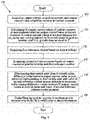
- the control method 100 includes steps 110 to 160.
- an output voltage of the grid-tie inverter and an output current value of the grid-tie inverter at the current moment are acquired.
- An output of the grid-tie inverter is a three-phase alternating current.
- the output voltage is represented by a function of V g .
- the output current is represented by a function of i g .
- the output current value at the current moment is i g (k), where k represents the current moment.
- N output current values of the grid-tie inverter at a next moment is calculated based on the output current value at the current moment, where the N output current values at the next moment are in one-to-one correspondence to N switch states of the grid-tie inverter, and N is a natural number greater than or equal to 2.
- a first reference current is acquired based on the output voltage.
- the first reference current is a current expected to be outputted by the grid-tie inverter. Therefore, similarly to the output current, the first reference current is a three-phase alternating current, which is represented by a function of i_ref1.
- a second reference current is acquired based on the output current of the grid-tie inverter and the first reference current.
- the second reference current is represented by a function of i_ref2.
- the second reference current is actually a current with a compensation added on the basis of the first reference current i_ref1, because the obtaining of the second reference current is further based on the output current of the grid-tie inverter, which means errors and disturbances of the system are fed back to the input end and the obtained final reference current includes a compensation that can cancel the errors and disturbances.
- a first switch state is determined from the N switch states, where a difference value between an output current value at the next moment corresponding to the first switch state and a value of the second reference current at the next moment is a minimum value among difference values between the N output current values at the next moment and the value of the second reference current at the next moment.
- the grid-tie inverter is controlled to perform power transmission in the first switch state at the next moment.
- a value of the second reference current with the compensation at the next moment is used, so that the obtained output current value at the next moment is more accurate.
- control method 100 will be further described below in conjunction with a working principle diagram and a schematic diagram of a topological structure of the grid-tie inverter.
- the output of the grid-tie inverter is a three-phase alternating current.
- the output voltage is a voltage across the capacitor in Fig. 2 , which can be obtained by a sensor and represented by a function of V g .
- the output current is the branch i g in Fig. 2 , that is, a difference value between a grid-tie current flowing through the inductor in Fig. 2 and a current flowing through the capacitor in Fig. 2 , which may be obtained by a sensor and represented by a function of i g .
- the output current value at the current moment is i g (k), where k represents the current moment.
- the output voltage V g of the grid-tie inverter and the output current value i g (k) at the current moment are acquired through the sensor.
- N output current values i g (k+1) of the grid-tie inverter at the next moment are calculated based on the acquired output current value i g (k) at the current moment.
- the N output current values i g (k+1) at the next moment is in one-to-one correspondence with the N switch states of the grid-tie inverter.
- a topological structure of an embodiment shown in Fig. 3 is taken as an example for illustrating how to obtain the N output current values i g (k+1) at the next moment.
- Fig. 3 exemplarily illustrates a schematic diagram of a topological structure of an embodiment of the grid-tie inverter according to the present application.
- the grid-tie inverter is a single-phase grid-tie inverter including four switches S1, S2, S3, and S4, which may be, for example, MOS transistors.
- the grid-tie inverter according to the present application is not limited to the above-mentioned form, and accordingly, the switch combination is not limited to the above-mentioned S1, S2, S3, and S4.
- the grid-tie inverter according to the present application may also be a three-phase grid-tie inverter including six switches.
- each of the four switches S1, S2, S3, and S4 is in an ON state (denoted as “1") or an OFF state (denoted as "0").
- the following four switch states of the grid-tie inverter may be obtained.
- the output current value i g (k+1) at the next moment calculated based on the output current value i g (k) at the current moment is different from that in each of the other switch states.
- Table 1 Switch state Number S1 S2 S3 S4 Switch state 1 1 0 0 1 Switch state 2 1 0 1 0 Switch state 3 0 1 1 0 Switch state 4 0 1 0 1
- the step 120 includes sub-step 1202 and sub-step 1204 as shown in Fig. 4 .
- N switch output voltages are obtained, respectively, based on the N switch states and an input voltage of the grid-tie inverter.
- Table 2 is based on the topological structure shown in Fig. 3 .
- the relationship between the switch states and the switch output voltages will be different.
- the N output current values i g (k+1) at the next moment are acquired, based on the output current value at the current moment i g (k), values U 0 (k) of the N switch output voltages at the current moment, and a value V g (k) of the output voltage V g of the grid-tie inverter at the current moment.
- Equation (3) obtained according to Euler's formula is submitted into above Equation (2) given above, so that the output current value i g (k+1) of the grid-tie inverter at the next moment may be obtained, where T s is a control frequency of the grid-tie inverter.
- the N output current values i g (k+1) at the next moment may be calculated according to Equation (4) given above. Specifically, for the topological structure shown in Fig. 3 , values (U dc , 0, -U dc , and 0) of U0 corresponding to the switch states 1 to 4 listed in Table 2 at the current moment are substituted into Equation (4) to obtain four output current values at the next moment: i g (k+1)_1, i g (k+1)_2, i g (k+1)_3 and i g (k+1)_4 .
- the first reference current i_ref1 is also acquired based on the output voltage V g , which corresponds to step 130 in the control method 100.
- the grid phase of the grid-tie inverter is also to be considered in the obtaining of the first reference current i_ref1.
- the output voltage V g is to be used.
- the step 130 includes sub-step 1302 and sub-step 1304 as shown in Fig. 5 .
- the grid phase of the grid-tie inverter is obtained based on the output voltage V g .
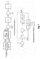
- the obtaining can be realized by a phase-locked loop.
- a phase-locked loop based on a generalized second-order integrator is needed.
- Fig. 7 shows the phase-locked loop and the generalized second-order integrator.
- a single-phase voltage component V g passes through the generalized second-order integrator, and two orthogonal voltage phasors V gsin and V gcos are generated.
- the voltage phasors are converted to a dq axis through dq left-side transformation.
- a q-axis reactive component becomes 0 through a pi controller, phase locking is achieved, and an output ⁇ is the grid phase.
- the expected output current value i expected may be a value in the range of 0 to 30 A, for example.
- the second reference current i_ref2 is acquired based on the output current i g of the grid-tie inverter and the first reference current i_ref1, which corresponds to step 140 in the control method 100.
- the step 140 includes sub-step 1402 and sub-step 1404 as shown in Fig. 6 .
- a third-order state model is established based on the output current i g of the grid-tie inverter.
- the LC filter included in the grid-tie inverter shown in Fig. 2 is a second-order system.
- the third-order state model is established on the basis of the second-order LC system.
- the expanded system model is the disturbance of the system. That is, the estimated system disturbance is obtained.
- a second reference current is obtained based on the established third-order state model and the first reference current. That is, the obtained disturbance output is compensated to the first reference current, and the second reference current obtained thereby includes the compensation value for the system disturbance. Feeding the compensated reference current (that is, the second reference current) to the predictive control according to the above method can significantly reduce the THD value and the direct current input (direct current input, DCI) value of the grid-tie current, thereby greatly improving the stability and robustness of predictive control.
- the expanded system model described above is a third-order state model because its corresponding grid-tie inverter includes a second-order LC system, but other expanded state models can be established based on configurations of specific grid-tie inverters. For example, if the grid-tie inverter includes a third-order LCL system, a fourth-order state model is needed to be established based on the output current i g . Similarly, the expanded system model is the disturbance of the system.
- L represents the inductance in Fig. 2
- i 1 is the current flowing through all of the inductors (that is, a grid-tie current)
- S represents ON/OFF states of the respective switches in Fig. 2 ("OFF” is recorded as “1”, “ON” is recorded as "0”).
- S can be expressed as ( S 1 ⁇ S 3 - S 2 ⁇ S 4)
- U dc is a voltage across the battery in Fig. 3 (that is, a direct current input voltage of the grid-tie inverter)
- U ac is a voltage across the capacitor in Fig.
- C represents a capacitance in Fig. 3
- i g is the output current of the grid-tie inverter
- d is a differential function.
- the output y of the above expanded state model is the reference current in an ideal situation, that is, the first reference current i_ref1 with no system disturbance being considered.
- the output current i g can be directly regarded as the grid-tie current i 1 .
- the above third-order state model and the functional expression of the second reference current i_ref2 calculated on the basis of the third-order state model are not unique. Based on different grid-tie inverter structures, other forms of third-order state models may be established, and different functional expressions of the second reference current i_ref2 may be calculated accordingly.
- a switch state corresponding to the minimum difference value between i g (k+1) and i_ref2(k+1) may then be determined from the N switch states corresponding to the N output current values i g (k+1) at the next moment. That is, the switch state in which i g (k+1) is closest to i_ref2(k+1) is identified.
- difference values between i g (k+1)_1 and i_ref2(k+1), between i g (k+1)_2 and i_ref2(k+1), between i g (k+1)_3 and i_ref2(k+1), and between i g (k+1)_4 and i_ref2(k+1) are calculated respectively.
- the switch state 2 is the switch state to be identified.
- the switch state to be identified may be obtained by setting a cost function and optimizing the cost function.
- the above cost function G is optimized so that the value obtained is the smallest.
- G is optimized so that the switch state corresponding to i g (k+1) when G takes the minimum value is the switch state to be identified.
- the difference between the output current value i g (k+1) at the next moment and the value i_ref2(k+1) of the second reference current at the next moment is amplified, so that the determined switch state can more accurately match the expected output current of the grid-tie inverter.
- the above cost function G is merely an example, and various forms of cost functions may be adopted by the control method according to the present application, as long as the i_ref2(k+1) closest to i g (k+1) can be identified through the cost functions.
- the switch state 2 is the switch state to be identified, then the four switches S1 to S4 may be set to "ON”, “OFF”, “ON”, and "OFF” at the next moment according to Table 1, thereby controlling the power transmission of the grid-tie inverter at the next moment.
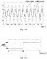
- Fig. 11(a) illustrates a waveform simulation diagram of an output current and an output voltage obtained by performing model predictive control on a grid-connected inverter using a conventional method.
- Fig. 1 1(b) illustrates a waveform simulation diagram of an output current and an output voltage obtained by performing model predictive control on a grid-connected inverter using the control method according to the present application. It can be clearly seen from these figures that, the resulting output current and output voltage by using the control method according to the present application are more stable.
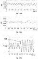
- Fig. 12(a) to Fig. 12(d) exemplarily illustrate comparison of output currents resulted from model predictive control on a grid-tie inverter using a conventional method and resulted from model predictive control on the grid-tie inverter using the control method according to the present application when voltage jump occurs.
- Fig. 12 (a) shows that the input voltage on the DC side of the grid-tie inverter jumps from 380V to 500V at the time of 0.5 seconds.
- Fig. 12 (b) using a conventional method for model predictive control on the grid-tie inverter
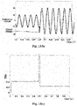
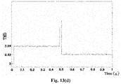
- Fig. 13(a) to Fig. 13(d) exemplarily illustrate comparison of THD values of output currents resulted from model predictive control on a grid connected inverter using a conventional method and resulted from model predictive control on the grid connected inverter using the control method according to the present application when the reference current abruptly changes.
- Fig. 13 (a) shows a reference current waveform when a reference current value abruptly changes from 10A to 20A at a certain timing in the conventional method.
- Fig. 13 (b) shows a reference current waveform when a reference current value (corresponding to the first reference current in the present application) abruptly changes from 10A to 20A at a certain timing in the control method according to the present application.
- Fig. 13 (a) shows a reference current waveform when a reference current value (corresponding to the first reference current in the present application) abruptly changes from 10A to 20A at a certain timing in the control method according to the present application.
- Fig. 13 (c) is a corresponding THD waveform in the case of Fig. 13 (a) .
- Fig. 13 (d) is a corresponding THD waveform in the case of Fig. 13 (b) .
- control method may be implemented by a processor executing computer instructions, and the instructions may be stored in a computer-readable storage medium.
- the computer-readable storage medium may include a hard disk drive, a floppy disk drive, a compact disk read/write (CD-R/W) drive, a digital versatile disk (DVD) drive, a flash drive, and/or a solid-state storage device, etc.
- a control apparatus for a grid-tie inverter is also provided correspondingly.
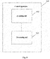
- a control apparatus 800 for a grid-tie inverter which includes an acquiring unit 810 and a processing unit 820.
- the acquiring unit 810 is configured to acquire an output voltage of the grid-tie inverter and an output current value of the grid-tie inverter at the current moment.
- the output voltage is the voltage across the capacitor in Fig. 2 , which may be obtained by a sensor and represented by the function of V g .
- the output current is the branch i g in Fig. 2 , that is, the difference value between the grid-tie current flowing through the inductor in Fig. 2 and the current flowing through the capacitor in Fig. 2 , which may be obtained by a sensor and represented by the function of i g .
- the output current value at the current moment is i g (k), where k represents the current moment.
- the processing unit 820 is configured to implement the following functions: calculating N output current values, i g (k+1)_1 , i g (k+1)_2,...,i g (k+1)_N, of the grid-tie inverter at a next moment based on the output current value i g (k) at the current moment, where the N output current values at the next moment are in one-to-one correspondence to N switch states of the grid-tie inverter, and N is greater than or equal to 2; acquiring a first reference current i_ref1 based on the output voltage V g , and acquiring a second reference current i_ref2 based on the output current V g of the grid-tie inverter and the first reference current i_ref1; determining a first switch state from the N switch states, where a difference value between the output current value i g (k+1) at the next moment corresponding to the first switch state and a value of the second reference current i_
- the processing unit 820 is configured to: establish a third-order state model based on an output current i g of the grid-tie inverter; and acquire the second reference current i_ref2 based on the established third-order state model and the first reference current i_ref1, where the second reference current includes a compensation value for a system disturbance.
- the processing unit 820 may be configured to: obtain N switch output voltages, U0_1, U0_2,...,U0_N, respectively, based on the N switch states and an input voltage of the grid-tie inverter; and obtain the N output current values, i g (k+1)_1, i g (k+1)_2,..., i g (k+1)_N, at the next moment, based on the output current value i g (k) at the current moment, values, U0(k)_1, U0(k)_2,..., U0(k)_N, of the N switch output voltages at the current moment, and a value V g (k) of the output voltage of the grid-tie inverter at the current moment.
- the N output current values, i g (k+1)_1, i g (k+1)_2 whili g (k+1)_N, at the next moment may be calculated according to Equation (10) given above.
- the processing unit 820 is configured to: obtain a grid phase ⁇ of the grid-tie inverter based on the output voltage V g ; and acquire the first reference current i_ref1 based on the grid phase ⁇ .
- control apparatus 800 implements the control method according to the present application as described above. Many design concepts and details described above applicable to the control method according to the present application are also applicable to the control apparatus 800 described above, and same beneficial technical effects can be obtained, which will not be repeated here.
- a grid-tie inverter system 900 is also provided, as shown in Fig. 9 .
- the grid-tie inverter system 900 includes a grid-tie inverter 910 and a control apparatus 920.
- the control apparatus 920 corresponds to the control apparatus 800 described above.
- the acquiring unit 922 in the control apparatus 920 corresponds to the acquiring unit 810 as described above, and is configured to acquire an output voltage V g of the grid-tie inverter 910, an output current i g , and the output current value i g (k) at the current moment.
- the processing unit 924 (corresponding to the processing unit 820 as described above) in the control apparatus 920 is then configured to determine the ON/OFF state which the grid-tie inverter 910 should be in at the next moment through a series of processing and calculations, and make the grid-tie inverter 910 perform power transmission at the next moment in this switch state.
- the grid-tie inverter system 900 has excellent robustness and stability, and the THD value and DCI value of the grid-tie current are significantly reduced compared with the prior art.
- V2G system 1000 there is also provided a V2G system 1000, as shown in Fig. 10 , where the V2G system 1000 includes a grid-tie inverter system 1010 corresponding to the above-described grid-tie inverter system 900. Therefore, the power transmission from the car battery 1100 to the public grid 1200 can be realized more stably and accurately.
Landscapes
- Engineering & Computer Science (AREA)
- Power Engineering (AREA)
- Transportation (AREA)
- Mechanical Engineering (AREA)
- Inverter Devices (AREA)
- Power Conversion In General (AREA)
Claims (10)
- Procédé pour commander un onduleur raccordé au réseau, comprenant :acquérir (110) une tension de sortie de l'onduleur raccordé au réseau et une valeur d'un courant de sortie de l'onduleur raccordé au réseau à un moment actuel ;calculer (120) N valeurs du courant de sortie de l'onduleur raccordé au réseau à un moment suivant basé sur la valeur du courant de sortie au moment actuel, dans lequel les N valeurs du courant de sortie au moment suivant sont en correspondance univoque avec N états de commutateur de l'onduleur raccordé au réseau, et N est un entier naturel supérieur ou égal à 2 ; etobtenir (1302) une phase de réseau de l'onduleur raccordé au réseau basé sur la tension de sortie, et acquérir (1304) un premier courant de référence basé sur la phase de réseau,établir (1402) un modèle d'état de tri-ordre basé sur un courant de sortie de l'onduleur raccordé au réseau ;acquérir (1404) un deuxième courant de référence basé sur le modèle d'état de tri-ordre et le premier courant de référence, dans lequel le deuxième courant de référence comprend une valeur de compensation pour une perturbation du système ;déterminer (150) un premier état de commutateur en fonction des N états de commutateur, dans lequel une valeur de différence entre la valeur du courant de sortie au moment suivant correspondant au premier état de commutateur et une valeur du deuxième courant de référence au moment suivant est une valeur minimale parmi les valeurs de différence entre les N valeurs du courant de sortie au moment suivant et la valeur du deuxième courant de référence au moment suivant ; etcommander (160) l'onduleur raccordé au réseau pour effectuer une transmission de puissance au premier état de commutateur au moment suivant, caractérisé en ce que le modèle d'état de tri-ordre est
 où X1 représente le courant de sortie ig de l'onduleur raccordé au réseau, X2 est une différentielle de X1, et X3 est une différentielle de X2 et représente la perturbation du système,le deuxième courant de référence est obtenu par l'équation suivante :
 où u représente le deuxième courant de référence, i ref1 est le premier courant de référence, kp = wc 2, kd = 2wc , wc est une fréquence de coupure de l'onduleur raccordé au réseau,
- Procédé selon la revendication 1, dans lequel l'étape de calculer N valeurs du courant de sortie de l'onduleur raccordé au réseau à un moment suivant basé sur la valeur du courant de sortie au moment actuel comprend :obtenir (1202) respectivement N tensions de sortie de commutateur, basé sur les N états de commutateur et une tension d'entrée de l'onduleur raccordé au réseau ; etobtenir (1204) les N valeurs du courant de sortie au moment suivant, basé sur la valeur du courant de sortie au moment actuel, des valeurs des N tensions de sortie de commutateur au moment actuel et une valeur de la tension de sortie de l'onduleur raccordé au réseau au moment actuel.
- Procédé selon la revendication 2, dans lequel les N valeurs du courant de sortie ig (K + 1) au moment suivant sont calculées par l'équation suivante :

- Dispositif (800) pour commander un onduleur raccordé au réseau, comprenant :une unité acquisition (810) configuré pour acquérir une tension de sortie de l'onduleur raccordé au réseau et une valeur d'un courant de sortie de l'onduleur raccordé au réseau à un moment actuel ; etune unité de traitement (820) configuré pourcalculer N valeurs du courant de sortie de l'onduleur raccordé au réseau à un moment suivant basé sur la valeur du courant de sortie au moment actuel, dans lequel les N valeurs du courant de sortie au moment suivant sont en correspondance univoque avec N états de commutateur de l'onduleur raccordé au réseau, et N est un entier naturel supérieur ou égal à 2 ; etobtenir une phase de réseau de l'onduleur raccordé au réseau basé sur la tension de sortie, et acquérir un premier courant de référence basé sur la phase de réseau,établir un modèle d'état de tri-ordre basé sur un courant de sortie de l'onduleur raccordé au réseau, et acquérir un deuxième courant de référence basé sur le modèle d'état de tri-ordre et le premier courant de référence, dans lequel le deuxième courant de référence comprend une valeur de compensation pour une perturbation du système ;déterminer un premier état de commutateur en fonction des N états de commutateur, dans lequel une valeur de différence entre la valeur du courant de sortie au moment suivant correspondant au premier état de commutateur et une valeur du deuxième courant de référence au moment suivant est une valeur minimale parmi les valeurs de différence entre les N valeurs du courant de sortie au moment suivant et la valeur du deuxième courant de référence au moment suivant ; etcommander l'onduleur raccordé au réseau pour effectuer une transmission de puissance au
 où X1 représente le courant de sortie ig de l'onduleur raccordé au réseau, X2 est une différentielle de X1, et X3 est une différentielle de X2 et représente la perturbation du système,le deuxième courant de référence est obtenu par l'équation suivante :
 où u représente le deuxième courant de référence, i ref1 est le premier courant de référence, kp = wc 2, kd = 2wc , wc est une fréquence de coupure de l'onduleur raccordé au réseau,
- Dispositif (800) selon la revendication 4, dans lequel l'unité de traitement (820) est configuré pourobtenir respectivement N tensions de sortie de commutateur, basé sur les N états de commutateur et une tension d'entrée de l'onduleur raccordé au réseau ; etobtenir les N valeurs du courant de sortie au moment suivant, basé sur la valeur du courant de sortie au moment actuel, des valeurs des N tensions de sortie de commutateur au moment actuel et une valeur de la tension de sortie de l'onduleur raccordé au réseau au moment actuel.
- Dispositif (800) selon la revendication 5, dans lequel les N valeurs du courant de sortie ig (K + 1) au moment suivant sont calculées par l'équation suivante :

- Dispositif (800) selon la revendication 4, dans lequel l'unité de traitement (820) est configuré pour
obtenir une phase de réseau de l'onduleur raccordé au réseau basé sur la tension de sortie, et acquérir un premier courant de référence basé sur la phase de réseau. - Système d'onduleur raccordé au réseau (900) comprenant :un onduleur raccordé au réseau (910) ; etun dispositif (920) selon l'une quelconque des revendications 4 à 7.
- Système de véhicule raccordé au réseau V2G (1000) comprenant le système d'onduleur raccordé au réseau (1010) selon la revendication 8.
- Support de stockage lisible par ordinateur sur lequel est stocké des instructions, dans lequel les instructions, lorsqu'elles sont exécutées par un processeur, met en oeuvre le procédé selon l'une quelconque des revendications 1 à 3 pour commander le dispositif selon l'une quelconque des revendications 4 à 7.
Applications Claiming Priority (2)
| Application Number | Priority Date | Filing Date | Title |
|---|---|---|---|
| CN202011284302.8A CN112104244B (zh) | 2020-11-17 | 2020-11-17 | 并网逆变器的控制方法和装置 |
| PCT/CN2021/075979 WO2022105068A1 (fr) | 2020-11-17 | 2021-02-08 | Procédé et dispositif de commande pour onduleur connecté au réseau |
Publications (3)
| Publication Number | Publication Date |
|---|---|
| EP4030611A1 EP4030611A1 (fr) | 2022-07-20 |
| EP4030611A4 EP4030611A4 (fr) | 2022-07-20 |
| EP4030611B1 true EP4030611B1 (fr) | 2022-12-21 |
Family
ID=80249460
Family Applications (1)
| Application Number | Title | Priority Date | Filing Date |
|---|---|---|---|
| EP21745203.6A Active EP4030611B1 (fr) | 2020-11-17 | 2021-02-08 | Procédé et dispositif de commande pour onduleur connecté au réseau |
Country Status (3)
| Country | Link |
|---|---|
| US (1) | US11251720B1 (fr) |
| EP (1) | EP4030611B1 (fr) |
| ES (1) | ES2936309T3 (fr) |
Families Citing this family (4)
| Publication number | Priority date | Publication date | Assignee | Title |
|---|---|---|---|---|
| CN114583702B (zh) * | 2022-05-05 | 2022-08-05 | 湖北工业大学 | Lcl型有源电力滤波器的并联电流控制系统及控制方法 |
| CN117039977B (zh) * | 2023-06-21 | 2024-06-11 | 淮阴工学院 | 一种基于预测控制条件下的模糊超螺旋滑模观测器电感辨识方法 |
| CN116707342B (zh) * | 2023-08-08 | 2023-12-19 | 安徽大学 | 一种数据驱动的储能逆变器电压预测控制方法 |
| CN118353082B (zh) * | 2024-04-23 | 2025-07-04 | 山东大学 | 一种并网逆变器无模型自适应协同控制方法及系统 |
Family Cites Families (33)
| Publication number | Priority date | Publication date | Assignee | Title |
|---|---|---|---|---|
| US7602627B2 (en) * | 2005-04-28 | 2009-10-13 | Origin Electric Company, Limited. | Electrical power source, operational method of the same, inverter and operational method of the same |
| JP4752352B2 (ja) * | 2005-06-24 | 2011-08-17 | トヨタ自動車株式会社 | 交流電圧出力装置およびそれを備えたハイブリッド自動車 |
| JP4707740B2 (ja) * | 2007-07-26 | 2011-06-22 | 三菱電機株式会社 | 電力変換装置 |
| US8279642B2 (en) * | 2009-07-31 | 2012-10-02 | Solarbridge Technologies, Inc. | Apparatus for converting direct current to alternating current using an active filter to reduce double-frequency ripple power of bus waveform |
| CN102598455B (zh) * | 2009-09-18 | 2017-06-20 | 金斯顿女王大学 | 分布式发电接口 |
| CN101710797B (zh) | 2009-12-07 | 2012-07-25 | 哈尔滨工业大学 | Z源型并网逆变器的电流预测无差拍控制方法及其控制装置 |
| US20120212064A1 (en) * | 2010-08-23 | 2012-08-23 | Array Converter Inc. | Methods and Devices for Controlling a Photovoltaic Panel in a Three Phase Power Generation System |
| TW201212463A (en) * | 2010-09-03 | 2012-03-16 | Chung Shan Inst Of Science | Stand-alone supply/grid-tie power inverter |
| JP5778445B2 (ja) * | 2011-03-11 | 2015-09-16 | 東芝機械株式会社 | インバータ発電装置 |
| US9071141B2 (en) * | 2011-04-08 | 2015-06-30 | Virginia Tech Intellectual Properties, Inc. | Two-stage single phase bi-directional PWM power converter with DC link capacitor reduction |
| CN201947196U (zh) | 2011-04-12 | 2011-08-24 | 中国科学院广州电子技术研究所 | 一种基于最大功率点跟踪的光伏并网逆变器 |
| US9698665B2 (en) * | 2012-09-14 | 2017-07-04 | Sparq Systems, Inc. | Digital controller for a power converter |
| EP2908416B1 (fr) * | 2013-12-24 | 2020-12-02 | LG Electronics Inc. | Dispositif d'entraînement par moteur et climatiseur comprenant celui-ci |
| US9887640B2 (en) * | 2014-05-09 | 2018-02-06 | Sparq Systems Inc. | DC-eliminating current controller for grid-connected DC/AC converters |
| CN104393620B (zh) | 2014-12-01 | 2016-08-24 | 江西仪能新能源微电网协同创新有限公司 | 一种预测电流光伏并网逆变器控制方法及装置 |
| US10396702B2 (en) * | 2015-02-12 | 2019-08-27 | Hitachi Automotive Systems, Ltd. | Motor drive control device |
| US9692320B2 (en) * | 2015-06-19 | 2017-06-27 | Sparq Systems Inc. | Adaptive control method for grid-connected inverters used with distributed power generation |
| US9570970B1 (en) * | 2015-07-24 | 2017-02-14 | Suzan EREN | Method and apparatus for use with grid connected inverters in distributed power generation |
| CN105515430A (zh) | 2016-01-15 | 2016-04-20 | 国网青海省电力公司 | 一种三相并网逆变器的控制方法 |
| WO2017168522A1 (fr) * | 2016-03-28 | 2017-10-05 | 三菱電機株式会社 | Convertisseur de puissance |
| JP6583109B2 (ja) * | 2016-04-12 | 2019-10-02 | 株式会社デンソー | 交流電動機の制御装置 |
| JP6471834B2 (ja) * | 2016-07-20 | 2019-02-20 | 日本精工株式会社 | 電動パワーステアリング装置 |
| KR101837742B1 (ko) | 2017-08-14 | 2018-03-13 | 주식회사 에너지파트너즈 | 무순단 절체 기능을 갖는 계통연계형 인버터 시스템 |
| US10971937B2 (en) * | 2017-09-26 | 2021-04-06 | The Governors Of The University Of Alberta | Grid-supporting inverters with significantly reduced storage requirements |
| CN108429286A (zh) | 2018-04-02 | 2018-08-21 | 武汉理工大学 | 一种基于自抗扰控制的并网电流调节器 |
| US11309786B2 (en) * | 2018-08-02 | 2022-04-19 | Polyvalor, Limited Partnership | Controller for power inverter |
| US10530267B1 (en) * | 2019-01-15 | 2020-01-07 | Cotek Electronic Ind. Co., Ltd. | Power converter |
| CN109921671B (zh) * | 2019-03-20 | 2020-09-04 | 中车青岛四方车辆研究所有限公司 | 单相逆变器并联控制方法、控制系统及逆变器 |
| CN109787495A (zh) | 2019-03-22 | 2019-05-21 | 福州大学 | 一种两电平逆变器的无模型预测电流控制方法 |
| CN110045610A (zh) | 2019-04-18 | 2019-07-23 | 中国地质大学(武汉) | 逆变器改进型多步模型预测控制方法、设备及存储设备 |
| CN110138253A (zh) | 2019-06-28 | 2019-08-16 | 盐城正邦环保科技有限公司 | 一种多谐振pr和pi联合控制的光伏并网逆变器控制方法 |
| CN112018809B (zh) | 2020-08-14 | 2022-03-08 | 长安大学 | 一种单相并网逆变器定频模型预测电流控制方法 |
| CN112104244B (zh) | 2020-11-17 | 2021-03-26 | 江苏时代新能源科技有限公司 | 并网逆变器的控制方法和装置 |
-
2021
- 2021-02-08 EP EP21745203.6A patent/EP4030611B1/fr active Active
- 2021-02-08 ES ES21745203T patent/ES2936309T3/es active Active
- 2021-09-27 US US17/485,554 patent/US11251720B1/en active Active
Also Published As
| Publication number | Publication date |
|---|---|
| EP4030611A1 (fr) | 2022-07-20 |
| US11251720B1 (en) | 2022-02-15 |
| ES2936309T3 (es) | 2023-03-16 |
| EP4030611A4 (fr) | 2022-07-20 |
Similar Documents
| Publication | Publication Date | Title |
|---|---|---|
| EP4030611B1 (fr) | Procédé et dispositif de commande pour onduleur connecté au réseau | |
| US10715056B2 (en) | Three-phase converter with zero-sequence regulation | |
| CN112104244B (zh) | 并网逆变器的控制方法和装置 | |
| CN109950922B (zh) | 一种适用于vsc-hvdc的多步模型预测控制方法 | |
| CN112217437A (zh) | 一种永磁同步电机三矢量模型预测电流控制电路和方法 | |
| CN110768280A (zh) | 一种并网逆变电流控制方法 | |
| Zamani et al. | Adaptive model predictive control for LCL-filter grid-tied inverters | |
| Avci et al. | Proportional multi‐resonant‐based controller design method enhanced with a lead compensator for stand‐alone mode three‐level three‐phase four‐leg advanced T‐NPC inverter system | |
| CN103997245A (zh) | 基于功率前馈和电流微差前馈的直流电压最小波动方法 | |
| CN107123991B (zh) | 基于模糊粒子群算法的动态电压恢复器控制方法及装置 | |
| CN116885787A (zh) | 不平衡电网下三电平逆变器多目标模型的预测控制方法 | |
| CN120033978B (zh) | 一种高增益比例谐振的pwm整流器直流电压纹波抑制方法 | |
| CN119335851B (zh) | 储能变流器控制器优化方法、设备、存储介质及产品 | |
| CN115276439A (zh) | 适应弱电网阻抗变化的lcl型并网逆变器谐振抑制方法 | |
| CN115241912B (zh) | 一种模型预测控制的三相并网逆变器模型失配补偿方法 | |
| CN119209733A (zh) | 基于降阶广义比例积分观测器的并网逆变器滑模控制方法 | |
| Yang et al. | Improved weighted average current control of LCL grid‐connected inverter and analysis of its order reduction characteristics | |
| CN114499257B (zh) | 一种低短路比下提高并网逆变器稳定性的控制方法 | |
| Guo et al. | A model-free direct predictive grid-current control strategy for grid-connected converter with an inductance-capacitance-inductance filter | |
| Fu et al. | High-performance finite-time adaptive control strategy for three-level t-type converters | |
| CN116632914A (zh) | 一种三电平pwm整流器三矢量无模型预测控制方法 | |
| Peng et al. | Optimization strategy and stability analysis of grid-connected inverter based on PLL positive sequence grid voltage feedforward in weak grid | |
| Xia et al. | Robust Control Method for LCL-Type Grid-Connected Inverters Based on Adaptive Correction of Grid Voltage Feedforward Considering Digital Control Delay | |
| Ray et al. | Small-signal impedance analysis of the impact of grid-forming controllers on their dc and ac dynamics | |
| CN117411068B (zh) | 基于双曲观测器的微网储能变流器互补超螺旋控制方法 |
Legal Events
| Date | Code | Title | Description |
|---|---|---|---|
| STAA | Information on the status of an ep patent application or granted ep patent |
Free format text: STATUS: UNKNOWN |
|
| STAA | Information on the status of an ep patent application or granted ep patent |
Free format text: STATUS: THE INTERNATIONAL PUBLICATION HAS BEEN MADE |
|
| PUAI | Public reference made under article 153(3) epc to a published international application that has entered the european phase |
Free format text: ORIGINAL CODE: 0009012 |
|
| STAA | Information on the status of an ep patent application or granted ep patent |
Free format text: STATUS: REQUEST FOR EXAMINATION WAS MADE |
|
| 17P | Request for examination filed |
Effective date: 20210802 |
|
| A4 | Supplementary search report drawn up and despatched |
Effective date: 20220222 |
|
| AK | Designated contracting states |
Kind code of ref document: A1 Designated state(s): AL AT BE BG CH CY CZ DE DK EE ES FI FR GB GR HR HU IE IS IT LI LT LU LV MC MK MT NL NO PL PT RO RS SE SI SK SM TR |
|
| RIC1 | Information provided on ipc code assigned before grant |
Ipc: B60L 55/00 20190101ALI20220817BHEP Ipc: H02M 7/5387 20070101ALI20220817BHEP Ipc: H02M 1/00 20060101ALI20220817BHEP Ipc: H02M 1/12 20060101ALI20220817BHEP Ipc: H02J 3/32 20060101ALI20220817BHEP Ipc: H02J 3/38 20060101ALI20220817BHEP Ipc: H02M 7/493 20070101ALI20220817BHEP Ipc: H02M 7/48 20070101AFI20220817BHEP |
|
| DAV | Request for validation of the european patent (deleted) | ||
| DAX | Request for extension of the european patent (deleted) | ||
| GRAP | Despatch of communication of intention to grant a patent |
Free format text: ORIGINAL CODE: EPIDOSNIGR1 |
|
| STAA | Information on the status of an ep patent application or granted ep patent |
Free format text: STATUS: GRANT OF PATENT IS INTENDED |
|
| INTG | Intention to grant announced |
Effective date: 20221013 |
|
| GRAS | Grant fee paid |
Free format text: ORIGINAL CODE: EPIDOSNIGR3 |
|
| GRAA | (expected) grant |
Free format text: ORIGINAL CODE: 0009210 |
|
| STAA | Information on the status of an ep patent application or granted ep patent |
Free format text: STATUS: THE PATENT HAS BEEN GRANTED |
|
| AK | Designated contracting states |
Kind code of ref document: B1 Designated state(s): AL AT BE BG CH CY CZ DE DK EE ES FI FR GB GR HR HU IE IS IT LI LT LU LV MC MK MT NL NO PL PT RO RS SE SI SK SM TR |
|
| REG | Reference to a national code |
Ref country code: GB Ref legal event code: FG4D |
|
| REG | Reference to a national code |
Ref country code: DE Ref legal event code: R096 Ref document number: 602021001043 Country of ref document: DE |
|
| REG | Reference to a national code |
Ref country code: CH Ref legal event code: EP |
|
| REG | Reference to a national code |
Ref country code: AT Ref legal event code: REF Ref document number: 1539639 Country of ref document: AT Kind code of ref document: T Effective date: 20230115 |
|
| REG | Reference to a national code |
Ref country code: IE Ref legal event code: FG4D |
|
| REG | Reference to a national code |
Ref country code: PT Ref legal event code: SC4A Ref document number: 4030611 Country of ref document: PT Date of ref document: 20230119 Kind code of ref document: T Free format text: AVAILABILITY OF NATIONAL TRANSLATION Effective date: 20230113 |
|
| REG | Reference to a national code |
Ref country code: ES Ref legal event code: FG2A Ref document number: 2936309 Country of ref document: ES Kind code of ref document: T3 Effective date: 20230316 |
|
| REG | Reference to a national code |
Ref country code: LT Ref legal event code: MG9D |
|
| REG | Reference to a national code |
Ref country code: NL Ref legal event code: MP Effective date: 20221221 |
|
| PG25 | Lapsed in a contracting state [announced via postgrant information from national office to epo] |
Ref country code: SE Free format text: LAPSE BECAUSE OF FAILURE TO SUBMIT A TRANSLATION OF THE DESCRIPTION OR TO PAY THE FEE WITHIN THE PRESCRIBED TIME-LIMIT Effective date: 20221221 Ref country code: NO Free format text: LAPSE BECAUSE OF FAILURE TO SUBMIT A TRANSLATION OF THE DESCRIPTION OR TO PAY THE FEE WITHIN THE PRESCRIBED TIME-LIMIT Effective date: 20230321 Ref country code: LT Free format text: LAPSE BECAUSE OF FAILURE TO SUBMIT A TRANSLATION OF THE DESCRIPTION OR TO PAY THE FEE WITHIN THE PRESCRIBED TIME-LIMIT Effective date: 20221221 Ref country code: FI Free format text: LAPSE BECAUSE OF FAILURE TO SUBMIT A TRANSLATION OF THE DESCRIPTION OR TO PAY THE FEE WITHIN THE PRESCRIBED TIME-LIMIT Effective date: 20221221 |
|
| REG | Reference to a national code |
Ref country code: AT Ref legal event code: MK05 Ref document number: 1539639 Country of ref document: AT Kind code of ref document: T Effective date: 20221221 |
|
| REG | Reference to a national code |
Ref country code: HU Ref legal event code: AG4A Ref document number: E061082 Country of ref document: HU |
|
| PG25 | Lapsed in a contracting state [announced via postgrant information from national office to epo] |
Ref country code: RS Free format text: LAPSE BECAUSE OF FAILURE TO SUBMIT A TRANSLATION OF THE DESCRIPTION OR TO PAY THE FEE WITHIN THE PRESCRIBED TIME-LIMIT Effective date: 20221221 Ref country code: LV Free format text: LAPSE BECAUSE OF FAILURE TO SUBMIT A TRANSLATION OF THE DESCRIPTION OR TO PAY THE FEE WITHIN THE PRESCRIBED TIME-LIMIT Effective date: 20221221 Ref country code: HR Free format text: LAPSE BECAUSE OF FAILURE TO SUBMIT A TRANSLATION OF THE DESCRIPTION OR TO PAY THE FEE WITHIN THE PRESCRIBED TIME-LIMIT Effective date: 20221221 Ref country code: GR Free format text: LAPSE BECAUSE OF FAILURE TO SUBMIT A TRANSLATION OF THE DESCRIPTION OR TO PAY THE FEE WITHIN THE PRESCRIBED TIME-LIMIT Effective date: 20230322 |
|
| P01 | Opt-out of the competence of the unified patent court (upc) registered |
Effective date: 20230522 |
|
| PG25 | Lapsed in a contracting state [announced via postgrant information from national office to epo] |
Ref country code: NL Free format text: LAPSE BECAUSE OF FAILURE TO SUBMIT A TRANSLATION OF THE DESCRIPTION OR TO PAY THE FEE WITHIN THE PRESCRIBED TIME-LIMIT Effective date: 20221221 |
|
| PG25 | Lapsed in a contracting state [announced via postgrant information from national office to epo] |
Ref country code: SM Free format text: LAPSE BECAUSE OF FAILURE TO SUBMIT A TRANSLATION OF THE DESCRIPTION OR TO PAY THE FEE WITHIN THE PRESCRIBED TIME-LIMIT Effective date: 20221221 Ref country code: RO Free format text: LAPSE BECAUSE OF FAILURE TO SUBMIT A TRANSLATION OF THE DESCRIPTION OR TO PAY THE FEE WITHIN THE PRESCRIBED TIME-LIMIT Effective date: 20221221 Ref country code: EE Free format text: LAPSE BECAUSE OF FAILURE TO SUBMIT A TRANSLATION OF THE DESCRIPTION OR TO PAY THE FEE WITHIN THE PRESCRIBED TIME-LIMIT Effective date: 20221221 Ref country code: CZ Free format text: LAPSE BECAUSE OF FAILURE TO SUBMIT A TRANSLATION OF THE DESCRIPTION OR TO PAY THE FEE WITHIN THE PRESCRIBED TIME-LIMIT Effective date: 20221221 Ref country code: AT Free format text: LAPSE BECAUSE OF FAILURE TO SUBMIT A TRANSLATION OF THE DESCRIPTION OR TO PAY THE FEE WITHIN THE PRESCRIBED TIME-LIMIT Effective date: 20221221 |
|
| PG25 | Lapsed in a contracting state [announced via postgrant information from national office to epo] |
Ref country code: SK Free format text: LAPSE BECAUSE OF FAILURE TO SUBMIT A TRANSLATION OF THE DESCRIPTION OR TO PAY THE FEE WITHIN THE PRESCRIBED TIME-LIMIT Effective date: 20221221 Ref country code: PL Free format text: LAPSE BECAUSE OF FAILURE TO SUBMIT A TRANSLATION OF THE DESCRIPTION OR TO PAY THE FEE WITHIN THE PRESCRIBED TIME-LIMIT Effective date: 20221221 Ref country code: IS Free format text: LAPSE BECAUSE OF FAILURE TO SUBMIT A TRANSLATION OF THE DESCRIPTION OR TO PAY THE FEE WITHIN THE PRESCRIBED TIME-LIMIT Effective date: 20230421 Ref country code: AL Free format text: LAPSE BECAUSE OF FAILURE TO SUBMIT A TRANSLATION OF THE DESCRIPTION OR TO PAY THE FEE WITHIN THE PRESCRIBED TIME-LIMIT Effective date: 20221221 |
|
| REG | Reference to a national code |
Ref country code: DE Ref legal event code: R097 Ref document number: 602021001043 Country of ref document: DE |
|
| PG25 | Lapsed in a contracting state [announced via postgrant information from national office to epo] |
Ref country code: MC Free format text: LAPSE BECAUSE OF FAILURE TO SUBMIT A TRANSLATION OF THE DESCRIPTION OR TO PAY THE FEE WITHIN THE PRESCRIBED TIME-LIMIT Effective date: 20221221 |
|
| REG | Reference to a national code |
Ref country code: BE Ref legal event code: MM Effective date: 20230228 |
|
| PLBE | No opposition filed within time limit |
Free format text: ORIGINAL CODE: 0009261 |
|
| STAA | Information on the status of an ep patent application or granted ep patent |
Free format text: STATUS: NO OPPOSITION FILED WITHIN TIME LIMIT |
|
| PG25 | Lapsed in a contracting state [announced via postgrant information from national office to epo] |
Ref country code: LU Free format text: LAPSE BECAUSE OF NON-PAYMENT OF DUE FEES Effective date: 20230208 Ref country code: DK Free format text: LAPSE BECAUSE OF FAILURE TO SUBMIT A TRANSLATION OF THE DESCRIPTION OR TO PAY THE FEE WITHIN THE PRESCRIBED TIME-LIMIT Effective date: 20221221 |
|
| 26N | No opposition filed |
Effective date: 20230922 |
|
| REG | Reference to a national code |
Ref country code: IE Ref legal event code: MM4A |
|
| PG25 | Lapsed in a contracting state [announced via postgrant information from national office to epo] |
Ref country code: SI Free format text: LAPSE BECAUSE OF FAILURE TO SUBMIT A TRANSLATION OF THE DESCRIPTION OR TO PAY THE FEE WITHIN THE PRESCRIBED TIME-LIMIT Effective date: 20221221 Ref country code: IE Free format text: LAPSE BECAUSE OF NON-PAYMENT OF DUE FEES Effective date: 20230208 |
|
| PG25 | Lapsed in a contracting state [announced via postgrant information from national office to epo] |
Ref country code: BE Free format text: LAPSE BECAUSE OF NON-PAYMENT OF DUE FEES Effective date: 20230228 |
|
| PG25 | Lapsed in a contracting state [announced via postgrant information from national office to epo] |
Ref country code: IT Free format text: LAPSE BECAUSE OF FAILURE TO SUBMIT A TRANSLATION OF THE DESCRIPTION OR TO PAY THE FEE WITHIN THE PRESCRIBED TIME-LIMIT Effective date: 20221221 |
|
| REG | Reference to a national code |
Ref country code: CH Ref legal event code: PL |
|
| PG25 | Lapsed in a contracting state [announced via postgrant information from national office to epo] |
Ref country code: CH Free format text: LAPSE BECAUSE OF NON-PAYMENT OF DUE FEES Effective date: 20240229 |
|
| PG25 | Lapsed in a contracting state [announced via postgrant information from national office to epo] |
Ref country code: CH Free format text: LAPSE BECAUSE OF NON-PAYMENT OF DUE FEES Effective date: 20240229 |
|
| PG25 | Lapsed in a contracting state [announced via postgrant information from national office to epo] |
Ref country code: BG Free format text: LAPSE BECAUSE OF FAILURE TO SUBMIT A TRANSLATION OF THE DESCRIPTION OR TO PAY THE FEE WITHIN THE PRESCRIBED TIME-LIMIT Effective date: 20221221 |
|
| PG25 | Lapsed in a contracting state [announced via postgrant information from national office to epo] |
Ref country code: BG Free format text: LAPSE BECAUSE OF FAILURE TO SUBMIT A TRANSLATION OF THE DESCRIPTION OR TO PAY THE FEE WITHIN THE PRESCRIBED TIME-LIMIT Effective date: 20221221 |
|
| PG25 | Lapsed in a contracting state [announced via postgrant information from national office to epo] |
Ref country code: CY Free format text: LAPSE BECAUSE OF FAILURE TO SUBMIT A TRANSLATION OF THE DESCRIPTION OR TO PAY THE FEE WITHIN THE PRESCRIBED TIME-LIMIT; INVALID AB INITIO Effective date: 20210208 |
|
| PG25 | Lapsed in a contracting state [announced via postgrant information from national office to epo] |
Ref country code: TR Free format text: LAPSE BECAUSE OF FAILURE TO SUBMIT A TRANSLATION OF THE DESCRIPTION OR TO PAY THE FEE WITHIN THE PRESCRIBED TIME-LIMIT Effective date: 20221221 |
|
| PGFP | Annual fee paid to national office [announced via postgrant information from national office to epo] |
Ref country code: GB Payment date: 20251218 Year of fee payment: 6 |
|
| PGFP | Annual fee paid to national office [announced via postgrant information from national office to epo] |
Ref country code: FR Payment date: 20251128 Year of fee payment: 6 |
|
| PGFP | Annual fee paid to national office [announced via postgrant information from national office to epo] |
Ref country code: HU Payment date: 20260122 Year of fee payment: 6 |
|
| PGFP | Annual fee paid to national office [announced via postgrant information from national office to epo] |
Ref country code: ES Payment date: 20260311 Year of fee payment: 6 |
|
| PGFP | Annual fee paid to national office [announced via postgrant information from national office to epo] |
Ref country code: DE Payment date: 20251216 Year of fee payment: 6 |
|
| PGFP | Annual fee paid to national office [announced via postgrant information from national office to epo] |
Ref country code: PT Payment date: 20260209 Year of fee payment: 6 |