EP4033366A1 - Optimisation de chemin d'accès de données - Google Patents
Optimisation de chemin d'accès de données Download PDFInfo
- Publication number
- EP4033366A1 EP4033366A1 EP22152830.0A EP22152830A EP4033366A1 EP 4033366 A1 EP4033366 A1 EP 4033366A1 EP 22152830 A EP22152830 A EP 22152830A EP 4033366 A1 EP4033366 A1 EP 4033366A1
- Authority
- EP
- European Patent Office
- Prior art keywords
- data path
- performance information
- access
- data
- access performance
- Prior art date
- Legal status (The legal status is an assumption and is not a legal conclusion. Google has not performed a legal analysis and makes no representation as to the accuracy of the status listed.)
- Granted
Links
Images


Classifications
-
- G—PHYSICS
- G06—COMPUTING OR CALCULATING; COUNTING
- G06F—ELECTRIC DIGITAL DATA PROCESSING
- G06F12/00—Accessing, addressing or allocating within memory systems or architectures
- G06F12/02—Addressing or allocation; Relocation
- G06F12/0223—User address space allocation, e.g. contiguous or non contiguous base addressing
- G06F12/0284—Multiple user address space allocation, e.g. using different base addresses
-
- G—PHYSICS
- G06—COMPUTING OR CALCULATING; COUNTING
- G06F—ELECTRIC DIGITAL DATA PROCESSING
- G06F13/00—Interconnection of, or transfer of information or other signals between, memories, input/output devices or central processing units
- G06F13/14—Handling requests for interconnection or transfer
- G06F13/16—Handling requests for interconnection or transfer for access to memory bus
-
- G—PHYSICS
- G06—COMPUTING OR CALCULATING; COUNTING
- G06F—ELECTRIC DIGITAL DATA PROCESSING
- G06F12/00—Accessing, addressing or allocating within memory systems or architectures
- G06F12/02—Addressing or allocation; Relocation
- G06F12/06—Addressing a physical block of locations, e.g. base addressing, module addressing, memory dedication
- G06F12/0607—Interleaved addressing
-
- G—PHYSICS
- G06—COMPUTING OR CALCULATING; COUNTING
- G06F—ELECTRIC DIGITAL DATA PROCESSING
- G06F12/00—Accessing, addressing or allocating within memory systems or architectures
- G06F12/02—Addressing or allocation; Relocation
- G06F12/08—Addressing or allocation; Relocation in hierarchically structured memory systems, e.g. virtual memory systems
-
- G—PHYSICS
- G06—COMPUTING OR CALCULATING; COUNTING
- G06F—ELECTRIC DIGITAL DATA PROCESSING
- G06F3/00—Input arrangements for transferring data to be processed into a form capable of being handled by the computer; Output arrangements for transferring data from processing unit to output unit, e.g. interface arrangements
- G06F3/06—Digital input from, or digital output to, record carriers, e.g. RAID, emulated record carriers or networked record carriers
- G06F3/0601—Interfaces specially adapted for storage systems
- G06F3/0602—Interfaces specially adapted for storage systems specifically adapted to achieve a particular effect
- G06F3/061—Improving I/O performance
-
- G—PHYSICS
- G06—COMPUTING OR CALCULATING; COUNTING
- G06F—ELECTRIC DIGITAL DATA PROCESSING
- G06F3/00—Input arrangements for transferring data to be processed into a form capable of being handled by the computer; Output arrangements for transferring data from processing unit to output unit, e.g. interface arrangements
- G06F3/06—Digital input from, or digital output to, record carriers, e.g. RAID, emulated record carriers or networked record carriers
- G06F3/0601—Interfaces specially adapted for storage systems
- G06F3/0628—Interfaces specially adapted for storage systems making use of a particular technique
- G06F3/0629—Configuration or reconfiguration of storage systems
- G06F3/0635—Configuration or reconfiguration of storage systems by changing the path, e.g. traffic rerouting, path reconfiguration
-
- G—PHYSICS
- G06—COMPUTING OR CALCULATING; COUNTING
- G06F—ELECTRIC DIGITAL DATA PROCESSING
- G06F3/00—Input arrangements for transferring data to be processed into a form capable of being handled by the computer; Output arrangements for transferring data from processing unit to output unit, e.g. interface arrangements
- G06F3/06—Digital input from, or digital output to, record carriers, e.g. RAID, emulated record carriers or networked record carriers
- G06F3/0601—Interfaces specially adapted for storage systems
- G06F3/0668—Interfaces specially adapted for storage systems adopting a particular infrastructure
- G06F3/0671—In-line storage system
- G06F3/0673—Single storage device
-
- G—PHYSICS
- G06—COMPUTING OR CALCULATING; COUNTING
- G06F—ELECTRIC DIGITAL DATA PROCESSING
- G06F3/00—Input arrangements for transferring data to be processed into a form capable of being handled by the computer; Output arrangements for transferring data from processing unit to output unit, e.g. interface arrangements
- G06F3/06—Digital input from, or digital output to, record carriers, e.g. RAID, emulated record carriers or networked record carriers
- G06F3/0601—Interfaces specially adapted for storage systems
- G06F3/0668—Interfaces specially adapted for storage systems adopting a particular infrastructure
- G06F3/0671—In-line storage system
- G06F3/0683—Plurality of storage devices
-
- G—PHYSICS
- G06—COMPUTING OR CALCULATING; COUNTING
- G06F—ELECTRIC DIGITAL DATA PROCESSING
- G06F2212/00—Indexing scheme relating to accessing, addressing or allocation within memory systems or architectures
- G06F2212/10—Providing a specific technical effect
- G06F2212/1016—Performance improvement
- G06F2212/1024—Latency reduction
-
- G—PHYSICS
- G06—COMPUTING OR CALCULATING; COUNTING
- G06F—ELECTRIC DIGITAL DATA PROCESSING
- G06F2212/00—Indexing scheme relating to accessing, addressing or allocation within memory systems or architectures
- G06F2212/15—Use in a specific computing environment
- G06F2212/154—Networked environment
-
- G—PHYSICS
- G06—COMPUTING OR CALCULATING; COUNTING
- G06F—ELECTRIC DIGITAL DATA PROCESSING
- G06F2212/00—Indexing scheme relating to accessing, addressing or allocation within memory systems or architectures
- G06F2212/25—Using a specific main memory architecture
- G06F2212/254—Distributed memory
- G06F2212/2542—Non-uniform memory access [NUMA] architecture
-
- G—PHYSICS
- G06—COMPUTING OR CALCULATING; COUNTING
- G06F—ELECTRIC DIGITAL DATA PROCESSING
- G06F2212/00—Indexing scheme relating to accessing, addressing or allocation within memory systems or architectures
- G06F2212/50—Control mechanisms for virtual memory, cache or TLB
- G06F2212/502—Control mechanisms for virtual memory, cache or TLB using adaptive policy
Definitions
- This relates to data access path optimization.
- Data is stored on one or more persistent storage devices, such as a number of drives.
- the data When data is to be written, the data is written via a data path onto the persistent storage device.
- the data When data is to be read, the data is read from a persistent storage device via a data path and returned to the data requester.
- a method comprising: obtaining a list of data paths to at least one persistent storage device through a plurality of NUMA nodes; associating with each data path, access performance information; receiving a request to access one of the at least one persistent storage device; calculating a preferred data path to the one of the at least one persistent storage device using the access performance information; and accessing the one of the at least one persistent storage device using the preferred data path.
- the method further comprising updating the access performance information of the used data path.
- the access performance information of each data path includes at least the last update time of the access performance information.
- the method further comprising: identifying data paths for testing; testing the identified data paths; and updating the access performance information of the tested data path.
- identifying data paths for testing further comprises: calculating the age of the access performance information using the last update time; and identifying data paths for testing having access performance information exceeding an age threshold.
- identifying data paths for testing further comprises selecting a percentage of all data paths for testing.
- identifying data paths for testing further comprises selecting all the data paths that have an error for testing.
- the access performance information of each data path includes at least a latency of the data path.
- the preferred data path is calculated based on at least the latency of the data path.
- the access performance information of each data path includes at least an average bandwidth indicator of the data path.
- the preferred data path is calculated based on at least the average bandwidth indicator of the data path.
- the access performance information of each data path includes at least a load on the data path.
- the preferred data path is calculated based on at least the load on the data path.
- the access performance information of each data path includes at least a reliability indicator of the data path.
- the preferred data path is calculated based on at least the reliability indicator on the data path.
- the access is read access.
- the access is write access.
- a system comprising: a memory; a plurality of NUMA nodes, each NUMA node comprising: at least one CPU core; and at least a portion of the memory is attached to the at least one CPU core, wherein the memory comprises instructions which, when executed by the plurality of NUMA nodes, configures the plurality of NUMA nodes to perform the method the first example embodiment.
- a computer software product comprising instructions which, when executed by one or more processors, cause the one or more processors to perform the method the first example embodiment.
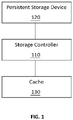
- the persistent storage device is a system for storing data in a persistent manner and may comprise one or more drives in different configurations.
- the storage controller 110 is in communication with a persistent storage device 120.
- the persistent storage device 120 is a system for storing data in a persistent manner. Although the persistent storage device is shown as a single component, in practice it may comprise multiple drives (such as hard disk drives or solid drive drives) arranged into groups and may be distributed over a number of storage nodes. Data is stored across the drives and may have error correcting encoding applied to reduce the risk of data loss if a component of the persistent storage device 120 fails.
- Data is stored on the persistent storage devices 120 in blocks.
- a block is a unit of data of predetermined size, such as 4 KiB (4096 bytes).
- the storage controller 110 is configured to use logical block addressing (LBA) when receiving requests to interact with the persistent storage device 120.
- LBA provides that each block of data stored on the persistent storage device 120 is identified by a unique integer LBA value.
- the storage controller 110 may translate an LBA value to determine which physical location on which persistent storage device the data is actually stored on.
- the storage controller 110 is further in communication with a cache 130.
- the cache comprises non-volatile memory chips configured to operate as a non-volatile cache. This may involve the use of flash memory alone or in combination with conventional volatile memory.
- the non-volatile memory chips may be configured as non-volatile dual in-line memory modules (NVDIMM).
- the storage controller is described as a single component, in practice the different functions of the storage controller may be split across different entities. For example, interactions with the cache 130 may occur through a cache controller independent of the storage controller 110.
- NUMA Non-Uniform Memory Access
- memory access time depends on the memory location relative to each processor. In some implementations memory access time depends on the memory location relative to particular cores of a processor. Further access time to particular I/O controllers and the peripherals connected to the I/O controllers can be relative to a particular processor or particular cores of a processor.
- a NUMA node may be a single CPU (central processing unit), a group of CPUs, a CPU core or a group of CPU cores.
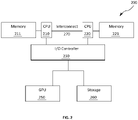
- FIG. 2 shows an example NUMA system.
- the system 200 comprises at least two CPUs 210, 220, memory associated with each CPU (local memory) 211, 221, an I/O Controller 230 and one or more peripherals connected to the I/O controller.
- the peripherals may include at least one GPU (graphics processing unit) 250 and persistent storage device 260.
- the CPUs 210, 220 are connected by an interconnect 270.
- the interconnect 270 allows CPUs 210, 220 to access the local memory associated with the other CPU.
- CPU 210 uses the interconnect 270 to access memory 221 associated with CPU 220.
- the system 300 comprises at least two CPUs 310, 320, memory associated with each CPU 311, 321 (local memory), two I/O controllers 331 and 332 and one or more peripherals connected to each I/O controller 331, 332.
- the peripherals may include at least one GPU (graphics processing unit) 351, 352 and persistent storage devices 361, 362 associated with each respective I/O controller 331, 332.
- the CPUs 310, 320 are connected by an interconnect 370.
- the interconnect 370 allows CPUs 310, 320 to access the local memory of the other CPU.
- CPU 310 uses the interconnect 370 to access memory 321 associated with CPU 320.
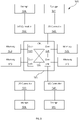
- FIG. 4 shows another alternative implementation.
- the system 400 comprises at least two CPUs 410, 420, memory associated with each CPU 411, 421 (local memory), I/O controller 412 and 422 associated with each CPU (local I/O controller) and one or more peripherals connected to each I/O controller 412, 422 (local peripherals).
- peripherals For simplicity the only peripherals shown in Figure 4 are persistent storage devices 416, 426 (local persistent storage devices). However other peripherals may be used in the implementation shown in Figure 4 .
- the CPUs 410, 420 are connected by an interconnect 470.
- the interconnect 470 allows CPUs 410, 420 to access the local memory and local peripherals associated and with the other CPU. For example, CPU 410 uses the interconnect 470 to access memory 421 associated with CPU 420. CPU 410 also uses the interconnect 470 to access local persistent storage device 426 associated with CPU 420.
- FIG. 5 shows yet another alternative implementation.
- the system 500 comprises at least one CPU 505 having a plurality of CPU cores 510, 520, 530 and 540, memory associated with each CPU core 511, 521, 531 and 541 (local memory), I/O controllers 512, 522, 532 and 542 (local I/O controllers) and one or more peripherals connected to each I/O controller (local peripherals).
- peripherals For simplicity the only peripherals shown in Figure 5 are persistent storage devices 516, 526, 536 and 546 (local persistent storage devices). However other peripherals may be used in the implementation shown in Figure 5 .
- the CPU cores 510, 520, 530 and 540 are connected by an interconnect 570.
- the interconnect 570 allows CPU cores 510, 520, 530 and 540 to access local memory and local peripherals associated and with the other CPU cores 510, 520, 530 and 540.
- CPU core 510 uses the interconnect 570 to access local memory 521 associated with CPU core 520.
- CPU core 520 uses the interconnect 570 to access local persistent storage device 546 associated with CPU 540.
- FIG. 5 has been illustrated with respect to CPU cores it can equally be applicable to multiple CPUs. Further each CPU core 510, 520, 530, and 540 has been illustrated as having a local I/O controller 512, 522, 532 and 542 associated with the respective core510, 520, 530, and 540, alternatively a group of CPU cores may share an I/O controller. In another alternative a group of CPU cores 510, 520, 530, and 540 may share local memory. In a similar manner a group of CPU cores may share access to a shared local persistent storage device.
- NUMA system there can be a number of paths from the respective CPUs or CPU cores to persistent storage devices.
- the storage controller is configured to administer access data (reading and writing data) from the persistent storage devices.
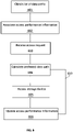
- Figure 6 shows an example approach through which the storage controller can access data.
- the storage controller obtains a list of data paths to one or more persistent storage devices through a plurality of NUMA nodes having associated CPU or CPU cores, memory and I/O controllers.
- the storage controller obtains the list of data paths by requesting from the system the data paths to the persistent storage devices.
- the storage controller associates access performance information with each of the data paths in the list.
- Access performance information may include the last update time of the access performance information, the latency of the data path, an average bandwidth indicator of the data path, the current load on the data path, and a reliability indicator of the data path.
- the storage controller receives a request to access one of the persistent storage devices.
- the access request may be a request to read data or to write data or to both read and write data.
- the request comprises an indication of the data to be read or written and an LBA value to indicate the location on one persistent storage device of the data to be read or the location on one persistent storage device that the data should be stored.
- the storage controller calculates the preferred data path to the persistent storage device to be accessed using the access performance information.
- the storage controller calculates the preferred path using the available access performance information including one or more of the latency of the data path, an average bandwidth indicator of the data path, the current load on the data path, and a reliability indicator of the data path.
- the storage controller accesses the persistent storage device to be accessed using the preferred data path.
- the storage controller updates the access performance information of the used data path.
- Access performance information that is updated may include the last update time of the access performance information, the latency of the data path, an average bandwidth indicator of the data path, the current load on the data path, and a reliability indicator of the data path.
- the access performance information is not updated for the used data path every time an access path is used.
- the access performance information may only be updated periodically.
- the storage controller updates the access performance information to indicate the error and returns 610 to step 604.
- the storage controller then recalculates the preferred data path to the persistent storage device to be accessed using the updated access performance information, including the error information.
- the storage controller may be configured to periodically test access performance and update access performance information.
- the frequency that the storage controller periodically tests access performance and update access performance information may be a set period and may depend on the number of access requests or depend on the system load.
- any other method for selecting the period that the storage controller periodically tests access performance and updates access performance information may be selected, including a combination of the above methods for setting the period.
- the storage controller may test all data paths and set or update access performance information for each data path.
- the access performance information may be stored on system shutdown and the storage controller may obtain the stored access performance information on system startup.
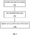
- Figure 7 shows an example approach by which the storage controller can test access.
- the storage controller identifies data paths for testing.
- the storage controller tests the identified data paths.
- the storage controller updates the access performance information of the tested data path.
- Data paths may be identified for test by calculating for each access path the age of the access performance information using the last update time.
- the last update time with typically be stored as the system access time but may be stored in any other suitable format.
- the storage controller using the age of the access performance information can identify paths for testing as those data paths having access performance information exceeding an age threshold.
- the age threshold may be a set age or alternatively the age threshold may be a calculated age such that the system identifies a percentage of all data paths as aged. The percentage may be any percentage but will typically be less than 50% of the data paths.
- the storage controller may identify data paths for testing by selecting a percentage of all data paths for testing.
- the storage controller may identify data paths for testing by selecting all the data paths that have an error for testing.
- processors may comprise a plurality of processors. That is, at least in the case of processors, the singular should be interpreted as including the plural. Where methods comprise multiple steps, different steps or different parts of a step may be performed by different processors.
Landscapes
- Engineering & Computer Science (AREA)
- Theoretical Computer Science (AREA)
- Physics & Mathematics (AREA)
- General Engineering & Computer Science (AREA)
- General Physics & Mathematics (AREA)
- Human Computer Interaction (AREA)
- Computer Networks & Wireless Communication (AREA)
- Debugging And Monitoring (AREA)
- Hardware Redundancy (AREA)
Applications Claiming Priority (1)
| Application Number | Priority Date | Filing Date | Title |
|---|---|---|---|
| US202163140606P | 2021-01-22 | 2021-01-22 |
Publications (2)
| Publication Number | Publication Date |
|---|---|
| EP4033366A1 true EP4033366A1 (fr) | 2022-07-27 |
| EP4033366B1 EP4033366B1 (fr) | 2026-05-06 |
Family
ID=80683161
Family Applications (1)
| Application Number | Title | Priority Date | Filing Date |
|---|---|---|---|
| EP22152830.0A Active EP4033366B1 (fr) | 2021-01-22 | 2022-01-21 | Optimisation de chemin d'accès de données |
Country Status (2)
| Country | Link |
|---|---|
| US (2) | US11860798B2 (fr) |
| EP (1) | EP4033366B1 (fr) |
Citations (2)
| Publication number | Priority date | Publication date | Assignee | Title |
|---|---|---|---|---|
| US20070083728A1 (en) * | 2005-10-11 | 2007-04-12 | Dell Products L.P. | System and method for enumerating multi-level processor-memory affinities for non-uniform memory access systems |
| EP3605331A1 (fr) * | 2017-08-07 | 2020-02-05 | Huawei Technologies Co., Ltd. | Procédé d'attribution de mémoire et serveur |
Family Cites Families (6)
| Publication number | Priority date | Publication date | Assignee | Title |
|---|---|---|---|---|
| US8041915B1 (en) | 2003-06-11 | 2011-10-18 | Globalfoundries Inc. | Faster memory access in non-unified memory access systems |
| US7472234B2 (en) | 2006-02-28 | 2008-12-30 | Red Hat, Inc. | Method and system for reducing latency |
| US7581064B1 (en) | 2006-04-24 | 2009-08-25 | Vmware, Inc. | Utilizing cache information to manage memory access and cache utilization |
| US7743140B2 (en) | 2006-12-08 | 2010-06-22 | International Business Machines Corporation | Binding processes in a non-uniform memory access system |
| US20150262632A1 (en) * | 2014-03-12 | 2015-09-17 | Fusion-Io, Inc. | Grouping storage ports based on distance |
| US9792212B2 (en) | 2014-09-12 | 2017-10-17 | Intel Corporation | Virtual shared cache mechanism in a processing device |
-
2022
- 2022-01-21 US US17/581,061 patent/US11860798B2/en active Active
- 2022-01-21 EP EP22152830.0A patent/EP4033366B1/fr active Active
-
2023
- 2023-11-17 US US18/512,254 patent/US12204467B2/en active Active
Patent Citations (2)
| Publication number | Priority date | Publication date | Assignee | Title |
|---|---|---|---|---|
| US20070083728A1 (en) * | 2005-10-11 | 2007-04-12 | Dell Products L.P. | System and method for enumerating multi-level processor-memory affinities for non-uniform memory access systems |
| EP3605331A1 (fr) * | 2017-08-07 | 2020-02-05 | Huawei Technologies Co., Ltd. | Procédé d'attribution de mémoire et serveur |
Also Published As
| Publication number | Publication date |
|---|---|
| US12204467B2 (en) | 2025-01-21 |
| US20240202141A1 (en) | 2024-06-20 |
| US20220237130A1 (en) | 2022-07-28 |
| EP4033366B1 (fr) | 2026-05-06 |
| US11860798B2 (en) | 2024-01-02 |
Similar Documents
| Publication | Publication Date | Title |
|---|---|---|
| US20100037226A1 (en) | Grouping and dispatching scans in cache | |
| US12099736B2 (en) | Scalable architecture enabling large memory system for in-memory computations | |
| US20140181042A1 (en) | Information processor, distributed database system, and backup method | |
| CN111124262B (zh) | 独立盘冗余阵列(raid)的管理方法、设备和计算机可读介质 | |
| CN111666043B (zh) | 一种数据存储方法及设备 | |
| DE102018120964A1 (de) | Integrierte Schaltungsspeichervorrichtungen mit verbesserter Pufferspeichernutzung während Lese- und Schreiboperationen | |
| CN110851074B (zh) | 嵌入式参考计数器和特殊数据模式自动检测 | |
| CN109313593A (zh) | 存储系统 | |
| US20240289225A1 (en) | Methods and systems for power failure resistance for a distributed storage system | |
| US20240264945A1 (en) | Affinity-based cache operation for a persistent storage device | |
| CN117539403A (zh) | 逻辑块读干扰监管方法、装置、计算机设备及存储介质 | |
| US7418367B2 (en) | System and method for testing a cell | |
| US7734842B2 (en) | Computer-implemented method, apparatus, and computer program product for managing DMA write page faults using a pool of substitute pages | |
| US10268594B2 (en) | Implementing paging device selection based on wear-level data | |
| CN112748865B (zh) | 用于存储管理的方法、电子设备和计算机程序产品 | |
| US8806166B2 (en) | Memory allocation in a multi-node computer | |
| EP4033366A1 (fr) | Optimisation de chemin d'accès de données | |
| US10949359B2 (en) | Optimizing cache performance with probabilistic model | |
| US10379776B2 (en) | Operation interlocking in an address-sliced cache system | |
| CN118295834B (zh) | 一种故障定位方法及计算设备 | |
| US12487774B2 (en) | Board management controller and method for storing sensor data in board management controller | |
| JP4221046B2 (ja) | ボリューム管理方法及び装置 | |
| JP4128594B2 (ja) | ボリューム管理方法及び装置 | |
| US10747446B2 (en) | Computer system and storage device activation control method | |
| JP2026001785A (ja) | データ記録システム |
Legal Events
| Date | Code | Title | Description |
|---|---|---|---|
| PUAI | Public reference made under article 153(3) epc to a published international application that has entered the european phase |
Free format text: ORIGINAL CODE: 0009012 |
|
| STAA | Information on the status of an ep patent application or granted ep patent |
Free format text: STATUS: THE APPLICATION HAS BEEN PUBLISHED |
|
| AK | Designated contracting states |
Kind code of ref document: A1 Designated state(s): AL AT BE BG CH CY CZ DE DK EE ES FI FR GB GR HR HU IE IS IT LI LT LU LV MC MK MT NL NO PL PT RO RS SE SI SK SM TR |
|
| STAA | Information on the status of an ep patent application or granted ep patent |
Free format text: STATUS: REQUEST FOR EXAMINATION WAS MADE |
|
| 17P | Request for examination filed |
Effective date: 20230120 |
|
| RBV | Designated contracting states (corrected) |
Designated state(s): AL AT BE BG CH CY CZ DE DK EE ES FI FR GB GR HR HU IE IS IT LI LT LU LV MC MK MT NL NO PL PT RO RS SE SI SK SM TR |
|
| RAP3 | Party data changed (applicant data changed or rights of an application transferred) |
Owner name: DAEDALUS CLOUD LLC |
|
| STAA | Information on the status of an ep patent application or granted ep patent |
Free format text: STATUS: EXAMINATION IS IN PROGRESS |
|
| 17Q | First examination report despatched |
Effective date: 20250812 |
|
| GRAP | Despatch of communication of intention to grant a patent |
Free format text: ORIGINAL CODE: EPIDOSNIGR1 |
|
| STAA | Information on the status of an ep patent application or granted ep patent |
Free format text: STATUS: GRANT OF PATENT IS INTENDED |
|
| RIC1 | Information provided on ipc code assigned before grant |
Ipc: G06F 12/02 20060101AFI20251120BHEP Ipc: G06F 12/06 20060101ALI20251120BHEP Ipc: G06F 12/08 20160101ALI20251120BHEP Ipc: G06F 3/06 20060101ALI20251120BHEP |
|
| INTG | Intention to grant announced |
Effective date: 20251203 |
|
| GRAS | Grant fee paid |
Free format text: ORIGINAL CODE: EPIDOSNIGR3 |
|
| GRAA | (expected) grant |
Free format text: ORIGINAL CODE: 0009210 |
|
| STAA | Information on the status of an ep patent application or granted ep patent |
Free format text: STATUS: THE PATENT HAS BEEN GRANTED |