EP4033547A1 - Leuchtdiodengehäuseanordnung - Google Patents
Leuchtdiodengehäuseanordnung Download PDFInfo
- Publication number
- EP4033547A1 EP4033547A1 EP20866760.0A EP20866760A EP4033547A1 EP 4033547 A1 EP4033547 A1 EP 4033547A1 EP 20866760 A EP20866760 A EP 20866760A EP 4033547 A1 EP4033547 A1 EP 4033547A1
- Authority
- EP
- European Patent Office
- Prior art keywords
- light
- package assembly
- layer
- led chips
- emitting diode
- Prior art date
- Legal status (The legal status is an assumption and is not a legal conclusion. Google has not performed a legal analysis and makes no representation as to the accuracy of the status listed.)
- Pending
Links
Images





Classifications
-
- H—ELECTRICITY
- H10—SEMICONDUCTOR DEVICES; ELECTRIC SOLID-STATE DEVICES NOT OTHERWISE PROVIDED FOR
- H10W—GENERIC PACKAGES, INTERCONNECTIONS, CONNECTORS OR OTHER CONSTRUCTIONAL DETAILS OF DEVICES COVERED BY CLASS H10
- H10W90/00—Package configurations
-
- H—ELECTRICITY
- H10—SEMICONDUCTOR DEVICES; ELECTRIC SOLID-STATE DEVICES NOT OTHERWISE PROVIDED FOR
- H10H—INORGANIC LIGHT-EMITTING SEMICONDUCTOR DEVICES HAVING POTENTIAL BARRIERS
- H10H20/00—Individual inorganic light-emitting semiconductor devices having potential barriers, e.g. light-emitting diodes [LED]
- H10H20/80—Constructional details
- H10H20/85—Packages
-
- H—ELECTRICITY
- H10—SEMICONDUCTOR DEVICES; ELECTRIC SOLID-STATE DEVICES NOT OTHERWISE PROVIDED FOR
- H10H—INORGANIC LIGHT-EMITTING SEMICONDUCTOR DEVICES HAVING POTENTIAL BARRIERS
- H10H20/00—Individual inorganic light-emitting semiconductor devices having potential barriers, e.g. light-emitting diodes [LED]
- H10H20/80—Constructional details
- H10H20/85—Packages
- H10H20/852—Encapsulations
-
- H—ELECTRICITY
- H10—SEMICONDUCTOR DEVICES; ELECTRIC SOLID-STATE DEVICES NOT OTHERWISE PROVIDED FOR
- H10H—INORGANIC LIGHT-EMITTING SEMICONDUCTOR DEVICES HAVING POTENTIAL BARRIERS
- H10H20/00—Individual inorganic light-emitting semiconductor devices having potential barriers, e.g. light-emitting diodes [LED]
- H10H20/80—Constructional details
- H10H20/85—Packages
- H10H20/852—Encapsulations
- H10H20/853—Encapsulations characterised by their shape
-
- H—ELECTRICITY
- H10—SEMICONDUCTOR DEVICES; ELECTRIC SOLID-STATE DEVICES NOT OTHERWISE PROVIDED FOR
- H10H—INORGANIC LIGHT-EMITTING SEMICONDUCTOR DEVICES HAVING POTENTIAL BARRIERS
- H10H20/00—Individual inorganic light-emitting semiconductor devices having potential barriers, e.g. light-emitting diodes [LED]
- H10H20/80—Constructional details
- H10H20/85—Packages
- H10H20/857—Interconnections, e.g. lead-frames, bond wires or solder balls
-
- H—ELECTRICITY
- H10—SEMICONDUCTOR DEVICES; ELECTRIC SOLID-STATE DEVICES NOT OTHERWISE PROVIDED FOR
- H10H—INORGANIC LIGHT-EMITTING SEMICONDUCTOR DEVICES HAVING POTENTIAL BARRIERS
- H10H20/00—Individual inorganic light-emitting semiconductor devices having potential barriers, e.g. light-emitting diodes [LED]
- H10H20/80—Constructional details
- H10H20/85—Packages
- H10H20/8506—Containers
Definitions
- the present invention relates to a package assembly, in particular a light-emitting diode package assembly, and a light-emitting device having the light-emitting diode package assembly.
- LED light-emitting diode
- various display devices such as TVs, cellular phones, PCs , notebook PCs, personal digital assistants (PDAs), etc.
- PDAs personal digital assistants
- Reducing the size of LED devices can improve the resolution of the display, thus expanding the application fields of LED displays, such as cell phones, car panels, TVs, computers, video conferencing, etc.
- the mainstream displays use a package size of 2121 and 1010. With the development of technology, a package size of 0808 or even smaller has emerged.
- the object of the present invention is to provide an ultra-small pitch light-emitting diode package assembly that includes a plurality of pixel regions arranged in an m ⁇ n array, where m and n are integers greater than one.
- Each pixel region PX can be called as a pixel.
- a light-emitting diode package assembly includes a plurality of light-emitting units arranged in an m ⁇ n array, where m and n are integers and m ⁇ n ⁇ 4, each light-emitting unit including a first LED chip, a second LED chip and a third LED chip, each LED chip including a first surface, a second surface opposite to the first surface, a side surface interconnecting the first surface and the second surface, and an electrode set formed on the second surface, the electrode set including a first electrode and a second electrode, the first surface being a light-exiting surface; an encapsulation layer filling gaps between the LED chips and covering sidewalls of the LED chips; and a wiring layer formed on the second surface of the plurality of LED chips.
- the LED chips of each light-emitting unit are arranged in a column in a first direction, and the first electrode and the second electrode of each LED chip are arranged side by side in a second direction.
- the wiring layer connects in parallel the first electrodes of the first LED chip, second LED chip and third LED chip of two or more adjacent light-emitting units in a third direction, and connects in parallel the second electrodes of the first LED chip, second LED chip and third LED chip of two or more adjacent light-emitting units in a fourth direction, thereby electrically connecting the plurality of light-emitting units to form an all-in-one light-emitting module.
- the third direction is the same as the first direction and the fourth direction is the same as the second direction, or the third direction is the same as the second direction and the fourth direction is the same as the first direction.
- the LED package assembly does not have a package substrate for carrying the LED chips, and the LED chips are held in position by the encapsulation layer.
- a distance D1 between adjacent light-emitting units is 0.8 mm or less.
- N may be an integer greater than or equal to 4, such as 4, 6, 8, 9, 16, 32 or 64, etc.
- the package assembly also includes pads for external connections.
- the number of the pads P is n + m ⁇ a, where a is the number of LED chips for each light-emitting unit, and n ⁇ m.
- the LED package assembly includes a plurality of light-emitting units arranged in an m ⁇ n array, where m and n are integers and m ⁇ n ⁇ 2, each light-emitting unit including a first LED chip, a second LED chip and a third LED chip, each LED chip including a first surface, a second surface opposite to the first surface, a side surface interconnecting the first surface and the second surface, and an electrode set formed on the second surface, the electrode set including a first electrode and a second electrode, the first surface being a light-exiting surface, the LED chips of each light-emitting unit being arranged in a column in a first direction, the first electrode and the second electrode of each LED chip being arranged side by side in a second direction, the first electrodes and the second electrodes of two adjacent columns of the LED chips are in opposite positions; an encapsulation layer filling gaps between the LED chips and covering sidewalls of the LED chips; and a wiring layer formed on the second surface of the plurality of LED chips,
- the wiring layer connects in parallel the first electrodes of the first, second and third LED chips of two or more adjacent light emitting units in the first direction, and connects in parallel the second electrodes of the first, second and third LED chips of two or more adjacent light emitting units in the second direction, thereby electrically connecting the plurality of light emitting units to form an all-in-one light emitting module.
- the function and effect of the invention include that it adopts the form of packaging without substrate, in which the LED chips of multiple light-emitting units are held by an encapsulation layer, and the LED chips of the multiple light-emitting units are connected in series or in parallel by forming a multi-layer wiring layer on the back of the multi-layer light-emitting units.
- the first wiring layer connects the LED chips of multiple pixel regions in series and parallel, and through the via layer and the second wiring layer, rewiring is carried out to form an integrated thin and small-pitch light-emitting diode package assembly.
- the number of layers of the wiring layer is no more than four, which ensures that the product is thin and light, facilitating thin and light design of the end products.
- Another object of the present invention is to provide a small-pitch and high-reliability light-emitting diode package assembly.
- the light emitting diode package assembly comprises a plurality of LED chips spaced apart from each other, each LED chip comprising a first surface, a second surface opposite to the first surface, a side surface interconnecting the first surface and the second surface, and an electrode set formed on the second surface, the electrode set comprising a first electrode and a second electrode, the first surface being a light emitting surface; an encapsulation layer filling the gaps between the LED chips and covering sidewalls of the LED chips, exposing the first and second electrodes of the LED chips; and a wiring layer formed on the second surface of the LED chips.
- the wiring layer includes multiple layers of conductive wires.
- a first layer of conductive wires is connected to the electrode set of the LED chip, and the relationship between a minimum wire width W of each layer of wires and a thickness T of the layer is as follows: W ⁇ T ⁇ 2W.
- the package assembly does not have a package substrate for carrying the LED chips, and the LED chips are held in position by the package layer and is physically supported by the wiring layer and the encapsulation layer with sufficient strength, so the thickness T and minimum wire width W of the conductive wires of each layer of the wiring layer directly determines the reliability of the package assembly.
- the size of the package assembly and the distance between the chips determine the minimum wire width W of the conductive wires.
- the minimum wire widths W for individual layers of conductive wires are usually not exactly the same.
- the thicknesses of layers of the multilayer conductive wires are not the same.
- at least one layer of the multilayer conductive wires has a thickness of 50 ⁇ m or less and at least one layer has a thickness of 60 ⁇ m or more.
- the melting point of the multilayer conductive wires is 400°C or more.
- the multilayer conductive wires can be made of a single metal of fine conductivity, such as Ag, Cu, Ni, Al and other materials.
- the above metal materials can form metal bonds with the electrodes of the LED chip through processes such as electroplating, chemistry plating, printing, etc.
- a protective layer is provided on a surface of at least one layer of the multilayer conductive wires.
- the protective layer includes a material that is very thin and stable at high temperatures, preferably a material with resistance to electromigration, corrosion and oxidation.
- the protective layer has a thickness of 50 ⁇ 200 nm.
- the minimum wire width W of each layer of the multilayer conductive wires is 10 ⁇ m or more, for example, it may be 10 ⁇ 60 ⁇ m.
- the encapsulation layer is made of a colored material layer with a light transmittance preferably not higher than 30%, and fills the gaps between the multiple LED chips and covers the sidewalls of the LED chips, which can prevent the optical crosstalk between the LED chips.
- a transparent or translucent light-transmissive layer can be formed on the light-exiting surfaces of the multiple LED chips, which on the one hand can protect the light-exiting surfaces of the LED chips, and on the other hand can be used as a light scattering layer to produce a light scattering effect. It reduces dizziness when the LED package assembly is finally used in display panels.
- the light-transmitting layer may include a light-scattering material, such as scattering particles.
- the transmittance of the light-transmissive layer can be adjusted according to different needs so as to achieve the best display effect. For example, when applied to indoor display, a translucent material can be selected as the light-transmissive layer with a transmittance of preferably 40% ⁇ 80%, which further reduces dizziness. When applied to outdoor display, a transparent layer with a transmittance preferably above 70% can be selected.
- the thickness of the light-transmissive layer is preferably 20 ⁇ m or less, preferably 10 ⁇ m or less, such as 10 ⁇ m or less, and the light-exiting surfaces of LED chips are located at substantially the same height (the height difference is 10 ⁇ m or less), which is conducive to unifying the light-exiting surfaces and reducing light crosstalk between sidewalls when the pixel regions of the package assembly are significantly increased.
- the package assembly also comprises an insulating layer formed on the encapsulation layer and covering one or more layers of conductive wires of the wiring layer.
- the insulating layer comprises one or more layers, at least one layer of which has a hardness greater than that of the conductive wires.
- the plurality of LED chips form multiple light-emitting units arranged in a m ⁇ n array, which constitutes an N-in-one light-emitting module, where n and m are integers greater than 1.
- Each of the light-emitting units include a first LED chip, a second LED chip and a third LED chip.
- the distance between the light-emitting units is 1mm or less.
- a distance D1 between adjacent light-emitting units is preferably 0.8 mm or less.
- N may be an integer greater than or equal to 4, such as 4, 6, 8, 9, 16, 32 or 64, etc. The larger the value of N, the smaller the value of D1 is. For example, when N is 4-9, D1 can be 0.4-0.8, and when N is 8 or more, then D can be 0.1-0.4.
- the package assembly also includes pads for external connection.
- the number of the pads P is n + m ⁇ a, where a is the number of LED chips of each the light-emitting unit, and n ⁇ m.
- a light-emitting diode (LED) package assembly is provided, which is an LED package assembly without a substrate.
- the LED package assembly may comprise a plurality of light-emitting units arranged in an m ⁇ n array, where m and n are integers greater than 1.
- Each light-emitting unit includes a plurality of LED chips 100 of different wavelengths, preferably, for example, at least three LED chips emitting red light (R), green light (G), and blue light (B), respectively. It may also include an LED chip emitting white light (including a wavelength conversion layer), that is, a combination of RGBW is formed so that the brightness of a display can be enhanced, which is very beneficial for outdoor display.
- Each light-emitting unit is equivalent to a pixel region PX, which can also be referred to as a pixel.
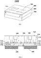
- the LED package assembly includes 2 ⁇ 2 pixel regions.
- Each pixel region PX includes a plurality of LED chips 100 spaced apart from one another and having an emitting surface S21.
- the package assembly also includes an encapsulation layer 200 that holds the plurality of LED chips 100 and fills gaps between the plurality of LED chips 100, and a multi-layer wiring layer located on the encapsulation layer.
- the multi-layer wiring layer includes a first wiring layer 310, a via layer 320 and a second wiring layer 330. Electrical isolation is provided between these layers by an insulating layer 500.
- the first wiring layer 310 is formed on the lower surfaces of the plurality of LED chips, connecting the plurality of LED chips in parallel and/or in series.
- the via layer 320 is formed on and electrically connected to the first wiring layer 310.
- the second wiring layer 330 is formed on and electrically connected to the via layer 320.
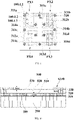
- FIG. 3 briefly illustrates the arrangement of the LED chips of the package assembly.
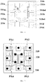
- the package assembly includes four pixel regions PX1 ⁇ PX4, each pixel region PX including a plurality of LED chips 100, such as a first LED chip 100L1, a second LED chip 100L2, and a third LED chip 100L3.
- each pixel region may also include only two LED chips or more than three LED chips, such as four LED chips.
- the three LED chips 100L1, 100L2, and 100L3 may emit light of different wavelengths, for example, they may emit red light, green light, and blue light, respectively.
- each of the above LED chips 100L1 ⁇ 100L3 has a pair of electrodes 110 on the same side, a first surface S21, a second surface S22 opposite to the first surface, a side surface S24 interconnecting the first surface S21 and the second surface S22, and an electrode surface S23.
- the first surface S21 is a light-exiting surface S21
- the second surface S22 is provided with the pair of electrodes 110.
- the LED chip includes a substrate 101, a first type semiconductor layer 121, a light-emitting layer 122 and a second type semiconductor layer 123.
- the first type semiconductor layer 121 and the second type semiconductor layer 123 may be p-type and n-type semiconductor layers, respectively.
- the LED chip also includes a transparent substrate 101 located on the first type semiconductor layer 121.
- the LED chip electrode set 110 includes a first electrode 111 electrically connected to the first type semiconductor layer 121, and a second electrode 112 electrically connected to the second type semiconductor layer 123.
- each LED chip electrode set 110 also includes a thickened layer of conductive material.
- the thickened layer is provided between the first electrode 111 and the first wiring layer, and between the second electrode 112 and the first wiring layer 310, respectively, and can be formed by electroplating, chemical plating or printing, etc.
- the material may be Cu, Cu x W or other conductive metal materials.
- the thickness of the electrode set of each LED chip is 5 ⁇ 200 ⁇ m, for example, it may be 5 ⁇ 30 ⁇ m, 30 ⁇ 50 ⁇ m, or 80 ⁇ 120 ⁇ m, depending on specific needs.
- the LED chip 100 may be an LED chip with a conventional size (a side of the chip is generally more than 200 ⁇ m), or Mini LED chip (the chip size is generally between 100 ⁇ 200 ⁇ m), or Micro LED chip (the chip size is generally no more than 100 ⁇ m). Mini LED chip or micro LED chip are preferable in the embodiment.
- the first, second and third chips LED-100L1 ⁇ 100-L3 in each pixel region PX of the package assembly are arranged in a straight line, and specifically, individual LED chips of each light-emitting unit are arranged in a column in a first direction, and the first and second electrodes of each LED chip are arranged side by side in a second direction, where the first direction and the second directions are substantially perpendicular to each other.
- the first electrode 111 and the second electrode 112 are in a left-right arrangement, the polarities of the electrodes of two adjacent columns of LED chips are opposite.
- the electrodes of the adjacent columns of chips are symmetrical, which can facilitate wiring and thereby reducing the distance between the chips.
- the polarities of the electrodes of the three LED chips 100L1 ⁇ 100L3 in the first pixel region PX1 are opposite to the polarities of the electrodes of the three LED chips 100L1 ⁇ L3 in the second pixel region PX2.
- the distance D1 for each pixel is preferably 1 mm, more preferably, 0.8 mm or less, for example, 0.1 ⁇ 0.3 mm, 0.3 ⁇ 0.5 mm, or 0.5 ⁇ 0.8 mm.
- the distance D2 between the chips in the same pixel region PX is preferably 100 ⁇ m or less, for example, 50 ⁇ 100 ⁇ m, or 50 ⁇ m or less.
- the distance between LED chips in the same pixel region is preferably 50 ⁇ m or less, for example, 40 ⁇ 50 ⁇ m, 30 ⁇ 40 ⁇ m, 20 ⁇ 30 ⁇ m, or 10 ⁇ 20 ⁇ m.
- a first encapsulation layer 200 is filled around the plurality of first, second, and third LED chips 100L1-100L3.
- the encapsulation layer 200 has a light transmittance of less than 30%. More preferably, the encapsulation layer 200 has a light transmittance of 5%-20%.
- the encapsulation layer 200 is opaque and nontransparent. Specifically, it includes light-absorbing component (not shown in the figures) provided at least around the sidewalls of the LED chips or between adjacent LED chips, or further at least around the LED semiconductor light-emitting stacked layers or between adjacent semiconductor light-emitting stacked layers.
- the light-absorbing component may specifically be light-absorbing particles dispersed within the epoxy resin or silicone of the encapsulation layer, such as black particles, or toner. Alternatively, the light-absorbing component may be a black resin.
- the light-absorbing component of the encapsulation layer 200 is provided at least around the sidewalls of the LED to prevent light-emitting form the side of the LED chips, thereby the emitted light of the LED chip is mainly from or all from the light-exiting surfaces of the LED chips, reducing crosstalk or mixing of light from different LED chips in the side direction.
- the encapsulation layer 200 may be epoxy resin or silicone with black colorant, so that all areas of the entire LED packaging assembly are black, except the light-exiting surface S21 of the LED chips 100, which helps to improve the contrast of display panel.
- each LED chip 100 is isolated through the black encapsulation material to reduce the light interference between individual LED chips.
- the hardness of the encapsulation layer 200 is preferably D60 or above, more preferably, D85 or more.
- a transparent or translucent material layer may be formed on the encapsulation layer 200 as another encapsulation layer 400, which covers the first surface S21 of the plurality of first, second, and third LED chips, preventing the LED chips from being exposed.
- the encapsulation layer 400 can be used as a light scattering lens to produce a light scattering effect. When the final LED packaging assembly is used in a display panel, it can effectively reduce the dizziness.
- the illustrated encapsulation layer 400 may include a light scattering material, such as scattering particles.
- the thickness of the encapsulation layer 400 is preferably between 5 - 20 ⁇ m, such as 10 ⁇ m, which, on the one hand, can protect the light-exiting surface of the LED chips, and on the other hand, with the encapsulation layer 200 using a light-absorbing material, can reduce the light interference between individual LED chips.
- the light transmittance is preferably 40% or more.
- the LED package assembly is used for indoor display, in which, the encapsulation layer 400 is preferably a translucent layer with a light transmittance of preferably 40% ⁇ 80%, more preferably 70 ⁇ 80%, which can reduce the brightness of the LED chip and thereby reduce light dizziness.
- the package assembly is used in the outdoor display, in which case the encapsulation layer 400 is preferably a transparent layer with a light transmittance of preferably 80% or more.
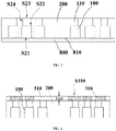
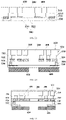
- the plurality of first, second, and third LED chips 100L1 ⁇ L3 may first be temporarily adhered to a support 800 such as a tape by taking the light-exiting surface S21 of the LED chips 100 as a die-bonding surface, and at this time, the electrode surface S23 is facing upward.
- a fluid insulating material is then filled between the chips and solidified as the encapsulation layer 200, exposing the electrode surface S23 of the LED chips. As shown in FIG.
- the thickness of the adhesive material 810 of the tape 800 is preferably controlled to be 5 ⁇ 20 ⁇ m, which on the one hand ensures that the LED chips will not be displaced when filling the encapsulation layer, and on the other hand ensures that the first surfaces S21 of the first, second and third LED chips 100L1 ⁇ L3 are substantially located at the same level with a height difference substantially below 10 ⁇ m, which unifies the light-exiting surfaces and reduces light crosstalk between sidewalls, while significantly increasing the pixel regions of the package assembly.
- the multi-layer wiring layer is formed on the second surfaces of the plurality of LED chips and includes multiple layers of conductive wires in this embodiment, the multiple layers of conductive wires specifically include a first wiring layer 310, a via layer 320, and a second wiring layer 330.
- the first wiring layer 310 is connected to the electrodes 110 of the LED chips
- the via layer 320 is formed on the first wiring layer 310
- the second wiring layer 330 is formed on the via layer 320 and is electrically connected to the first wiring layer 310 through the via layer 320.
- the multiple layers of conductive wires are preferably made of a metal material with a melting point higher than 400°C, such as Ag, Cu, Ni, Al, etc.
- the material of these layers may be the same or different, and may be formed by electroplating, chemical plating or printing, etc.
- the thickness of each layer is preferably 100 ⁇ m or less, such as 20 ⁇ 80 ⁇ m.
- the LED package assembly does not have a package substrate for carrying the LED chips, and the LED chips 100 are held in position by the encapsulation layer 200 and physically supported by the wiring layer 300 and the encapsulation layer with sufficient strength, so the wiring layer 300 needs to have a sufficient thickness for providing mechanical strength.
- the mechanical strength of the wiring layer can be increased by increasing the thickness of any layer of conductive wires, but the thickness of each layer of conductive wires should not be too large considering the need for exposure of the wires and the yield of thick electrode coating.
- the reliability of the wiring layer can be ensured by setting the relationship between the thickness T of each conductive wire of the wiring layer and the minimum wire width W of the conductive wire of the layer.
- the minimum wire width W depends on the size of the package assembly and the distance between the chips, which is preferably not less than 30 ⁇ m.
- the relationship between the minimum wire width W for each layer of wire and the thickness T of the layer is configured to be W ⁇ T ⁇ 2W.
- the thickness of each conductive wire is not less than the minimum wire width of the layer, which can ensure that the wiring layer 300 has sufficient thickness to provide mechanical strength for the device. Meanwhile, it is required that the thickness of any layer of the conductive wire T ⁇ 2W, so as to avoid a decrease in yield of any layer of the conductive wires duo to a large thickness thereof.
- the first wiring layer 310 is formed on the surface of the encapsulation layer 200 and are electrically connected to the electrodes 110 of the plurality of LED chips.
- An insulating layer 510 is filled in the gaps between the wires of the first wiring layer 310, exposing a surface S310 of the first wiring layer 310 away from the LED chips.
- the material of the insulating layer 510 may be the same as the material of the encapsulation layer 200, or different. When the same material is used, the insulating layer 510 and the encapsulation layer 200 form a single layer, and it is difficult to distinguish the two.
- the LED package assembly is used in a display device, and the insulating layer 510 and the encapsulation layer 200 are both epoxy resin or silicone with colorant.
- the hardness of the insulating layer 510 is not less than the hardness of the first wiring layer 310, for example, D60 or above, more preferably, D85 or above, which helps to expose the surface S310 of the first wiring layer 310 by grinding.
- the first wiring layer 310 includes a plurality of first wires and at least two common wires, thereby electrically connecting the LED chips of the multiple pixel regions PX to form an n-in-one pixel region.
- FIG. 7 illustrates an example of a four-in-one package assembly, in which the LED chips of four pixel regions are connected in series and/or parallel. In other embodiments, it is not limited to a four-in-one structure, but may also be a nine-in-one or sixteen-in-one, etc. In the package assembly shown in FIG. 7 , this first wiring layer 310 includes two common wires 314a, 314d and ten first wires.
- the first wires 311a ⁇ 311d are connected to the first electrodes 111 of the first chips 100-L1 of the pixel regions PX, respectively.
- the wires 313a ⁇ 313d are connected to the first electrodes 111 of the third chips 100-L3 of the PX.
- the wire 312a is connected to the first electrodes of the second LED chips 100-L2 ofPX1 and PX4.
- the wire 312b is connected to the first electrodes of the second LED chips 100-L2 of PX2 and PX3.
- the common wire 314a is connected to the second electrodes 112 of the first, second, and third LED chips of PX1 and PX2, and the common wire 314d is connected to the second electrodes 112 of the first, second, and third LED chips of PX3 and PX4.
- the thickness T310 of the first wiring layer 310 is preferably 1 ⁇ 2 times, preferably 1.2 ⁇ 1.8 times, the minimum wire width W1 of the first wiring layer.
- the via layer 320 is located on the surface S310 of the first wiring layer 310, including a plurality of vias 320 formed in an insulating layer 520.
- the number and location of the vias correspond to the individual wires of the first wiring layer.
- the pattern filled with solid diagonal lines in FIG. 9 represents the vias, which are as far away from each LED chip as possible.
- the material of the insulating layer 520 may be referred to the insulating layer 510.
- the thickness T320 of the via layer 320 is preferably less than 100 ⁇ m, and preferably 1 ⁇ 2 times the minimum wire width W2 of the via layer, for example, 1 ⁇ 1.2 times, 1.2 ⁇ 1.5 times, or 1.5 ⁇ 2 times, depending on different needs.
- the diameter of the via of the layer is equal to the minimum wire width W2 of the layer, and the diameter of the via is preferably 20 ⁇ 60 ⁇ m.
- the via layer is preferably 20 ⁇ 50 ⁇ m, for example, 25 ⁇ 30 ⁇ m, so as to avoid excessive stress and thermal resistance due to the large thickness of the via layer, and reduce the total thickness of the package structure, while ensuring the strength of the package structure, making the end products thinner and lighter.
- the via layer has a thickness of 50 ⁇ 80 ⁇ m, for example 60 ⁇ m, thus appropriately increasing the thickness of the package assembly and thus facilitating pickup of a device from a sidewall thereof.
- the second wiring layer 330 is located on the via layer 320 and forms an electrical connection with the first wiring layer 310 through the respective vias of the via layer 320.
- An insulating layer 530 is filled in the gaps between the wires of the third wiring layer 330, exposing a surface s330 of the second wiring layer 330 away from the LED chips.
- the material of the insulating layer 530 may be referred to the insulating layer 510.
- the wires of the third wiring layer 330 includes a plurality of connecting wires 331ac, 331bd, 333ac, 333bd and a plurality of connecting portions 331a, 331b, 332a, 332b, 333c, 333d, 334a and 334d.
- the connecting wires are used to connect the electrodes of the same type of LED chips and which have the same polarity.
- the connection 331ac connects the first electrodes 111 of the first LED chips 100-L1 of PX1 and PX3
- the connection 333ac connects the first electrodes 111 of the third LED chips 100-L3 of PX1 and PX3.
- the connecting portions can be used as electrode pads for external connection, for being connected to a power supply.
- a pad 600 can be made in the corresponding area of the connecting portion and the area outside the pad can be covered with ink, epoxy resin or other insulating material to protect the wires of the second wiring layer 330.
- the connecting portions of the second wiring layer 330 completely covers each via of the via layer 320, increasing the contact area between the second wiring layer and the vias.
- conductive material of the via layer and the second wiring layer can be formed in the same process, saving a process of forming conductive material and grinding, which can effectively save costs and improve product stability.
- the thickness T330 of the third wiring layer 330 is preferably 1 ⁇ 2 times, preferably 1.2 ⁇ 1.8 times, of the minimum wire width W3 of the third wiring layer.
- the insulating layers 510 ⁇ 530 may be of the same material or of different materials, specifically selected from epoxy resin, silicone, polyimide, benzocyclobutene, or PBO. When composed of the same material, the insulating layers 510 ⁇ 530 are combined into a single layer 500, which is difficult to distinguish them. In some specific embodiments, the insulating layers 510 ⁇ 530 are made of opaque or low-transmittance materials, such as epoxy resin or silicone doped with a black colorant, preventing or reducing the light emitted from the LED chips from a rewiring layer which may otherwise cause crosstalk.
- a metal wire pattern of the wiring layer can be formed first, then the insulating layer can be formed by filling, and finally the surface of the metal wires in the wiring layer can be exposed by grinding.
- the insulating layers 510 ⁇ 530 may be partially or fully light transmissive, and the transmittance is thus higher than the that of the encapsulation layer 200.
- the light-transmissive layer can be made without adding colorants or light-absorbing materials, such as toner or dyes, and is preferably a silicone or epoxy resin material layer that does not contain micron-sized particles (usually particles with a diameter of 1 micron or more, such as C-powder particles), so as to avoid a decrease in reliability (e.g., a decrease in insulation performance) otherwise caused by possible defects such as unevenness and interface defects due to the addition of colorants, which can ensure the reliability of the encapsulation of the insulating layer to the wiring layer.
- a photosensitive material is solidified to form the insulating layer, which simplifies the process. Meanwhile, the area around the chip and the non-metallic part of the electrode surface are covered with light-absorbing material as the encapsulation layer 200 to prevent crosstalk of light from the sides of the chips.
- FIG. 12 shows the connection relationship of the three wiring layers
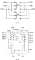
- FIG. 13 shows the equivalent circuit diagram of the four-in-one light-emitting unit.
- the four-in-one light-emitting unit is lead out by eight connecting portions 331a, 331b, 332a, 332b, 333c, 333d, 334a and 334d.
- the first electrodes of the first LED chip 100-L1 are led out by the connecting portions 331a and 331b
- the first electrodes of the second LED chips 100-L2 are led out by the connecting portions 332a and 332b
- the first electrodes of the third LED chips 100-L3 are led out by the connecting portions 333c and 333d.
- the connecting portions 334a and 334d connect the second electrodes 112 of all LED chips of PX1 to PX4, respectively.
- the LED chips in each PX are arranged in a straight line. Specifically, respective LED chips of each light-emitting unit are arranged in a column in a first direction. The first and second electrodes of each LED chip are arranged side by side in a second direction. The first and second directions are substantially perpendicular to each other. The polarities of the electrodes of two adjacent columns of LED chips are opposite.
- the common electrodes of the LED chips of two adjacent PX in left-right arrangement are connected into a common electrode, and the second LED chips 100-L2 (located in the middle of the three chips) of the two adjacent PX in the up-to-down direction are connected in parallel (i.e., the first electrodes of the second LED chips of PX1 and PX3 are connected in parallel and the first electrodes of the second LED chips of PX1 and PX4 are connected in parallel).
- the first LED chips 100-L1 and the third LED chips 100-L3 of PX1 ⁇ PX4 are individually wired to reduce the number of electrode terminals of the four-in-one light-emitting unit to 10.
- the first LED chips and the second LED chips of the two adjacent PX in the up-to-down direction are then connected in parallel by wires, respectively (i.e., the first electrodes of the first LED chips of PX1 and PX3 are connected in parallel to form an electrode terminal 331a, the first electrodes of the first LED chips of PX2 and PX4 are connected in parallel to form an electrode terminal 331b, the first electrodes of the third LED chips of PX1 and PX3 are connected in parallel to form an electrode terminal 334c , and the first electrodes of the third LED chip of PX2 and PX4 are connected in parallel to form an electrode terminal 334d).
- a total of 8 electrode terminals i.e., 8 connecting portions
- are led out which effectively reduces the number of electrode pads of the package assembly and thus facilitates placement of chips.
- the package assembly according to the above exemplary embodiment does not have a package substrate or holder for carrying the LED chips, the light-emitting units in the m ⁇ n array arrangement are mainly held and supported by insulating material layers (including 200, 400 and 500) and wiring layers.
- the thickness T of the package assembly depends mainly on the thickness TA of the LED chips and the thickness TC of the wiring layer. In some specific embodiments, mini-type LED chips are used which have a thickness TA between 40 ⁇ 150 ⁇ m.
- the thickness TC of the multi-layer wiring layer is between 30 ⁇ 200 ⁇ m, more preferably between 50 ⁇ 150 ⁇ m. T and TA meets the relationship: 1.4 ⁇ T/TA ⁇ 10.
- the circuit layer can avoid too much stress and too much thermal resistance, and make the total thickness of the package assembly smaller while ensuring the strength of the package structure.
- the thickness of the LED chip TA is approximately 80 ⁇ m
- the thickness of the package assembly can be 120 ⁇ m ⁇ 500 ⁇ m, for example, 120 ⁇ 200 ⁇ m
- the thickness of each sub-layer of the wiring layer can be 10 ⁇ 50 ⁇ m, ratio 40 ⁇ m.
- the small size of the package assembly e.g., 0.4mm ⁇ 0.4mm or smaller does not facilitate gripping from an upper surface of the package assembly.
- the thickness T of the package assembly can be increased appropriately so that the sidewall of the package assembly has a larger area for a pickup device to contact and grasp, and preferably, the thickness of the package assembly can be 150 ⁇ 500 ⁇ m, such as 180 ⁇ 360 ⁇ m.
- the thickness of the package assembly can be increased by increasing the thickness of the LED chip and/or the thickness of the wiring layer.
- the thickness of the electrodes of the LED chip may be increased and/or the thickness of each wiring layer may be appropriately increased.
- the thickness of the via layer is preferably 30 ⁇ 80 ⁇ m, and the thickness of the other wiring layers is preferably 50 ⁇ 100 ⁇ m.
- a micro-type LED chip is used, the thickness of the chip TA is between 5 and 10 ⁇ m, and the thickness of the multi-layer wiring layer TC is between 20 ⁇ m and 200 ⁇ m. More preferably, the thickness of the wiring layer TC is between 50 ⁇ m and 150 ⁇ m. T and TA satisfy the relation: 10 ⁇ T/TA ⁇ 60, for example, the thickness of the package assembly can be 50 ⁇ 100 ⁇ m, or 100 ⁇ 200 ⁇ m.
- FIGS. 14 ⁇ 17 show another embodiment of the LED package assembly of the present invention.
- the package assembly also includes a plurality of pixel regions PX1 ⁇ PX4 arranged in an m ⁇ n array.
- the LED chips in the pixel regions have the same polarity direction, which is conducive to improving the efficiency and accuracy of chip alignment.
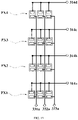
- the first wiring layer includes first wires 311a, 313c and common wires 314a, 314d.
- the second wiring layer includes connecting portions 331a, 331c, 332b, 332c, 333b, 333c, 334a, 334d and connecting wires 331cd, 332ab, 332cd, 333ab.
- 331cd connects the first LED chips 100-L1 of the horizontally adjacent pixel regions PX3 and PX4, 332ab connects the second LED chip 100-L2 of the horizontally adjacent pixel regions PX1 and PX2, 332ab connects the second LED chip 100-L2 of the horizontally adjacent pixel regions PX1 and PX2, and 333cd connects the third LED chips 100-L3 of the horizontally adjacent pixel regions PX3 and PX4.
- 17 shows an equivalent circuit diagram of the four-in-one package assembly, where 334a and 334d connect all LED chips of the light-emitting units located in the same column along the longitudinal direction, respectively, and 331a, 331c, 332b, 333b, 333c connect the same type of LED chips of light-emitting units located in the same row, respectively.
- FIG. 18 shows a further embodiment of the LED package assembly of the present invention.
- the LED device also includes four pixel regions PX1 ⁇ PX4 arranged in a 2 ⁇ 2 array, with each pixel region corresponding to a light-emitting unit.
- the LED chips of the pixel regions are arranged with the same polarity direction.
- the first wiring layer 330 includes conductive wires 314a and 314b, which connect the second electrodes 112 of all LED chips located in the same column, respectively.
- the second wiring layer includes conductive wires 331a ⁇ 333a and 331b ⁇ 333b, which connect the first electrodes 111 of the same type of LED chips located in the same row, respectively.
- the wire 331a connects the first electrodes 111-L1 of the first type of LED chips in the first row
- the wire 332a connects the first electrodes 111-L2 of the second type of LED chips in the first row
- the wire 331b connects the first electrodes 111-L1 of the first type of LED chips in the second row.
- the first wiring layer and the second wiring layer are separated from each other by an insulating layer, and are electrically connected to each other by via layer. The connections of wires of the first wiring layer and the second wiring layer can be switched.
- FIG.19 shows a further embodiment of the LED package assembly of the present invention.
- the LED device also includes four pixel regions PX1 ⁇ PX4, arranged in a 4 ⁇ 1 array.
- the LED package assembly is rectangular or approximately rectangular in shape, which facilitates assembly when applied to display devices and allows for a minimum number of pads for external connection through a wiring design.
- the first wiring layer includes wires 314a ⁇ 314d which connect in parallel the second electrodes of the light-emitting units of pixel regions PX1 ⁇ PX4 in the longitudinal direction, respectively and form four electrode terminals for external connection.
- the second wiring layer includes wires 331a ⁇ 333a which connect the same type of first, second, or third LED chips of pixel regions PX1 ⁇ PX4, and form three electrode terminals for external connection. In this way, the pixel regions PX1 ⁇ PX4 can form a four-in-one light-emitting module.
- the four-in-one LED package assembly change the arrangement of light-emitting units and uses 4 ⁇ 1 arrangement, in which the number of pads P for external connection is equal to 4+a, where a is the number of chips in a single light-emitting unit.
- each light-emitting unit includes three chips, i.e. a red LED chip 100-L1, a green LED chip 100-L2 and a blue LED chip 100-L3, so only 7 pads are needed, achieving the minimum number of pads, which reduces the size of the package assembly, while conducive to wiring, chip placement at the application end, and reducing the risk of short circuit.
- FIGS. 20 to 22 show a further embodiment of the LED package assembly of the present invention.
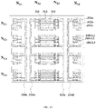
- FIG. 20 shows the arrangement of the LED chips and the first wiring layer of this LED package assembly.
- the LED device also includes 16 pixel regions PX1 ⁇ PX4 arranged in a 4 ⁇ 4 array.
- the distance D1 between the individual light-emitting units of the 16-in-1 LED package assembly is preferably 0.1 ⁇ 0.5 mm, for example, 0.2 ⁇ 0.5 mm.
- the LED chips of each light-emitting unit is first arranged in a column in a first direction, and the first and second electrodes of each LED chip are arranged side by side in a second direction, where the first and second directions are substantially perpendicular to each other.
- the second electrodes of all the LED chips located in the same column are connected in parallel, and in the second direction, the first electrodes of the same type of LED chips located in the same row are connected in parallel.
- the first and second electrodes of LED chips in adjacent columns are in opposite positions, which facilitates the parallel connection of the first electrodes of the same LED chips located in the same row, thus simplifying the wiring of the wiring layer.
- the first wiring layer includes common wires 314a ⁇ 314d, which are connected to the second electrodes of the LED chips of the columns N X1 ⁇ N X4 of light emitting units, respectively.
- the first wires include 311 ⁇ 313, where 311 connects the first electrodes of the first LED chips L1 located in the same row of columns N X2 and N X3 , 312 connects the first electrodes of the second LED chip L2 located in the same row of columns N X2 and N X3 , and 313 connects the first electrode of the third LED chip L3 located in the same row of columns N X2 and N X3 .
- the first wiring also includes wires 311a ⁇ 313a, which are connected to the first electrodes of the first, second and third LED chips in rows N X1 and N X4 , respectively.
- FIG. 21 shows a pattern of the via layer with a plurality of vias, out of which vias 324 are connected to the common wires 314a ⁇ 314d of the first wiring layer and vias 321 ⁇ 323 are connected to the first wiring of the first wiring layer, respectively.
- FIG. 22 shows a pattern of the second wiring layer including connecting wires 331 ⁇ 333 and connecting portions 331a ⁇ 333, 334.
- the connecting wire 331 connects in parallel the first electrodes of the first LED chips located in the same row
- the connecting wire 332 connects in parallel the first electrodes of the second LED chips located in the same row (e.g. rows N Y1 ⁇ N Y4 )
- the connecting wire 333 connects in parallel the third LED chips located in the same row.
- the connecting portions serve as terminals for external connection.
- 331a ⁇ 333a are connected to the connecting wires 331 ⁇ 333 respectively, and334 are connected to 324.
- pads can be made in the corresponding area of the connecting portion, and the area outside the pads is covered with ink, epoxy resin or other insulating material to protect the wires of the second wiring layer.
- the number of layers of the wiring layer is no more than four (including the pad layer for external connection), which ensures the product is thin and light and conducive to the thin and light end products.
- FIG. 23 shows an LED package assembly without a substrate.
- the encapsulation layer 200 covers both the sidewalls of the LED chips and the sidewall S311 of the first wiring layer 310.
- the encapsulation layer 200 is preferably opaque, or has a low light low transmittance, for example, less than 30%, such as 5 ⁇ 20%.
- the encapsulation layer is selected from black materials, such as epoxy resin or silicone with a black colorant.
- the insulating layers 520 and 530 can be made of light-transmissive or opaque materials.
- the LED package assembly uses the encapsulation layer to hold and encapsulate the pixel dots arranged in an array, and provides a multi-layer wiring layer to connect the LED chips of the pixels in series. Therefore, the present invention does not require solder wires and circuit board with precise wiring, improving reliability and contrast. In addition, the electrode set of the LED chip does not need to be soldered with solder paste onto the board, avoiding poor chip soldering and improving the integration of LED and electronic components, so it indeed achieves the purpose of this invention.
- FIG. 24 shows a structure of an LED package assembly of another embodiment of the present invention.
- a metal protective layer 700 is formed on the surface of one or more layers of conductive wires of the wiring layer, which on the one hand prevents metal diffusion of the conductive wires, and on the other hand provides corrosion and oxidation resistance.
- the protective layer has a thickness of 20 ⁇ 500 nm, and its material may be selected from titanium (Ti), titanium nitride (TiN), tungsten (W), tantalum (Ta), tantalum nitride (TaN), molybdenum (Mo), cobalt (Co), and platinum (Pt), etc.
- FIG. 25 shows a structure of an LED package assembly of a further embodiment of the present invention.
- the protective layer 700 covers both the surface and the sidewalls of the conductive wires.
- the protective layer can better protect the conductive wire, while increasing the adhesion of the wiring layer to the insulating layer 500.
Landscapes
- Led Device Packages (AREA)
- Engineering & Computer Science (AREA)
- Microelectronics & Electronic Packaging (AREA)
- Structures Or Materials For Encapsulating Or Coating Semiconductor Devices Or Solid State Devices (AREA)
- Devices For Indicating Variable Information By Combining Individual Elements (AREA)
Applications Claiming Priority (4)
| Application Number | Priority Date | Filing Date | Title |
|---|---|---|---|
| CN201921554474.5U CN210403768U (zh) | 2019-09-18 | 2019-09-18 | 发光二极管封装组件 |
| CN201921554475.XU CN210403726U (zh) | 2019-09-18 | 2019-09-18 | 发光二极管封装组件 |
| CN202020278177.9U CN211743151U (zh) | 2020-03-09 | 2020-03-09 | 发光二极管封装组件 |
| PCT/CN2020/098502 WO2021051924A1 (zh) | 2019-09-18 | 2020-06-28 | 发光二极管封装组件 |
Publications (2)
| Publication Number | Publication Date |
|---|---|
| EP4033547A1 true EP4033547A1 (de) | 2022-07-27 |
| EP4033547A4 EP4033547A4 (de) | 2023-10-25 |
Family
ID=74883938
Family Applications (1)
| Application Number | Title | Priority Date | Filing Date |
|---|---|---|---|
| EP20866760.0A Pending EP4033547A4 (de) | 2019-09-18 | 2020-06-28 | Leuchtdiodengehäuseanordnung |
Country Status (5)
| Country | Link |
|---|---|
| US (1) | US12230612B2 (de) |
| EP (1) | EP4033547A4 (de) |
| JP (1) | JP7601771B2 (de) |
| KR (1) | KR102694716B1 (de) |
| WO (1) | WO2021051924A1 (de) |
Families Citing this family (9)
| Publication number | Priority date | Publication date | Assignee | Title |
|---|---|---|---|---|
| CN115956299A (zh) | 2020-10-23 | 2023-04-11 | 东丽株式会社 | 显示装置及显示装置的制造方法 |
| CN113597256A (zh) * | 2021-07-29 | 2021-11-02 | 业成科技(成都)有限公司 | 显示模组及其制造方法 |
| KR102759226B1 (ko) * | 2022-08-01 | 2025-01-23 | 한국광기술원 | 마이크로 led 패키지 및 이를 구비한 디스플레이 |
| DE112021007529T5 (de) * | 2021-12-30 | 2024-02-29 | Hubei San'an Optoelectronics Co., Ltd. | Lichtemittierendes Modul, Verfahren zur Herstellung eines lichtemittierenden Moduls und Anzeigevorrichtung |
| TWI866601B (zh) * | 2022-08-29 | 2024-12-11 | 錼創顯示科技股份有限公司 | 發光顯示單元 |
| TWI835265B (zh) * | 2022-08-29 | 2024-03-11 | 錼創顯示科技股份有限公司 | 發光顯示單元及顯示裝置 |
| CN116885084B (zh) * | 2023-09-07 | 2023-12-15 | 元旭半导体科技(无锡)有限公司 | 一种自带封装基板的led芯片及其制备方法 |
| KR102895485B1 (ko) * | 2024-05-27 | 2025-12-12 | 주식회사 글로벌테크놀로지 | 광범위 발광 구동 패키지와, 백라이트 유닛 및 디스플레이 장치 |
| DE102024121537A1 (de) * | 2024-07-29 | 2026-01-29 | Starlight Display Corporation | Als Display verwendetes und mit reflektierendem Kolloid gefülltes Mini-LED-Lichtpaneel zur Erhöhung der Lichthelligkeit und dessen Mini-LED-Display |
Family Cites Families (19)
| Publication number | Priority date | Publication date | Assignee | Title |
|---|---|---|---|---|
| JP2009054913A (ja) * | 2007-08-29 | 2009-03-12 | Seiko Epson Corp | 照明装置及び液晶表示装置 |
| JP2010171170A (ja) * | 2009-01-22 | 2010-08-05 | Hitachi Cable Ltd | 銅回路配線基板およびその製造方法 |
| KR101926358B1 (ko) * | 2012-02-17 | 2018-12-07 | 삼성전자주식회사 | 반도체 발광장치 및 조명장치 |
| CN206558500U (zh) * | 2016-09-30 | 2017-10-13 | 深圳市玲涛光电科技有限公司 | 发光元件、背光源模组及电子设备 |
| KR102701861B1 (ko) * | 2016-11-15 | 2024-09-04 | 삼성디스플레이 주식회사 | 발광장치 및 그의 제조방법 |
| CN109216525B (zh) * | 2017-07-04 | 2021-08-10 | 英属开曼群岛商錼创科技股份有限公司 | 发光模块及显示装置 |
| FR3069378B1 (fr) * | 2017-07-21 | 2019-08-23 | Aledia | Dispositif optoelectronique |
| CN111048656B (zh) * | 2017-09-04 | 2024-06-14 | 首尔半导体株式会社 | 显示装置及该显示装置的制造方法 |
| WO2019066491A1 (ko) * | 2017-09-29 | 2019-04-04 | 서울반도체 주식회사 | 발광 소자 및 그것을 갖는 표시 장치 |
| KR102536305B1 (ko) * | 2018-01-05 | 2023-05-24 | (주)포인트엔지니어링 | 마이크로 led 구조체 및 이의 제조방법 |
| JP6799627B2 (ja) * | 2018-02-26 | 2020-12-16 | 山東捷潤弘光電科技有限公司 | Rgb−ledパッケージモジュール及びそのディスプレイ |
| CN108807356B (zh) * | 2018-06-05 | 2020-10-27 | 深圳市智讯达光电科技有限公司 | 一种四合一mini-LED模组、显示屏及制造方法 |
| CN109952641B (zh) * | 2019-01-15 | 2023-01-10 | 泉州三安半导体科技有限公司 | 发光二极管封装器件及发光装置 |
| KR102620829B1 (ko) * | 2019-08-27 | 2024-01-03 | 삼성전자주식회사 | 발광소자 패키지 및 이를 포함하는 디스플레이 장치 |
| CN210403726U (zh) * | 2019-09-18 | 2020-04-24 | 厦门三安光电有限公司 | 发光二极管封装组件 |
| CN210607242U (zh) * | 2019-09-18 | 2020-05-22 | 厦门三安光电有限公司 | 发光二极管封装组件 |
| CN210403768U (zh) * | 2019-09-18 | 2020-04-24 | 厦门三安光电有限公司 | 发光二极管封装组件 |
| CN210403724U (zh) * | 2019-09-18 | 2020-04-24 | 厦门三安光电有限公司 | 发光二极管封装组件 |
| US11695102B2 (en) * | 2020-06-19 | 2023-07-04 | Creeled, Inc. | Active electrical elements with light-emitting diodes |
-
2020
- 2020-06-28 JP JP2021542363A patent/JP7601771B2/ja active Active
- 2020-06-28 EP EP20866760.0A patent/EP4033547A4/de active Pending
- 2020-06-28 KR KR1020217021342A patent/KR102694716B1/ko active Active
- 2020-06-28 WO PCT/CN2020/098502 patent/WO2021051924A1/zh not_active Ceased
-
2022
- 2022-03-10 US US17/691,638 patent/US12230612B2/en active Active
Also Published As
| Publication number | Publication date |
|---|---|
| JP7601771B2 (ja) | 2024-12-17 |
| KR20210096270A (ko) | 2021-08-04 |
| US20220199592A1 (en) | 2022-06-23 |
| WO2021051924A1 (zh) | 2021-03-25 |
| EP4033547A4 (de) | 2023-10-25 |
| US12230612B2 (en) | 2025-02-18 |
| JP2022536436A (ja) | 2022-08-17 |
| KR102694716B1 (ko) | 2024-08-12 |
Similar Documents
| Publication | Publication Date | Title |
|---|---|---|
| EP4033547A1 (de) | Leuchtdiodengehäuseanordnung | |
| CN210403726U (zh) | 发光二极管封装组件 | |
| US10490533B2 (en) | Light emitting apparatus, illumination apparatus and display apparatus | |
| CN210403724U (zh) | 发光二极管封装组件 | |
| CN210403768U (zh) | 发光二极管封装组件 | |
| US20220139890A1 (en) | Light-emitting diode packaging module | |
| TWI590414B (zh) | 發光裝置 | |
| EP4016651A1 (de) | Lichtemittierende verkapselungsanordnung, lichtemittierendes modul und anzeigeschirm | |
| US20190189853A1 (en) | Light emitting device package | |
| EP4033529A1 (de) | Leuchtdiodenverpackungsanordnung | |
| US20240363599A1 (en) | Display substrate and preparation method therefor, and display apparatus | |
| CN210607242U (zh) | 发光二极管封装组件 | |
| CN210403725U (zh) | 发光二极管封装组件 | |
| WO2026067873A1 (zh) | 一种发光装置及显示装置 | |
| CN211743151U (zh) | 发光二极管封装组件 | |
| CN114156261A (zh) | 一种显示装置及其制作方法 | |
| CN222366574U (zh) | 一种mip芯片结构及显示面板 | |
| WO2024190226A1 (ja) | 積層構造体および半導体装置 | |
| CN118039621A (zh) | 一种显示组件及其制作方法 | |
| EP4734716A1 (de) | Lichtemittierende diode, anzeigevorrichtung damit und herstellungsverfahren dafür | |
| CN119208349A (zh) | 一种显示装置 | |
| CN118173694A (zh) | 发光芯片及其制备方法、发光基板及显示装置 | |
| CN119421579A (zh) | Led灯珠及其制备方法、显示屏 | |
| CN121531877A (zh) | 微型发光器件及其制作方法 | |
| CN113192940A (zh) | 一种混光均匀的三基色Mini LED背光源 |
Legal Events
| Date | Code | Title | Description |
|---|---|---|---|
| STAA | Information on the status of an ep patent application or granted ep patent |
Free format text: STATUS: THE INTERNATIONAL PUBLICATION HAS BEEN MADE |
|
| PUAI | Public reference made under article 153(3) epc to a published international application that has entered the european phase |
Free format text: ORIGINAL CODE: 0009012 |
|
| STAA | Information on the status of an ep patent application or granted ep patent |
Free format text: STATUS: REQUEST FOR EXAMINATION WAS MADE |
|
| 17P | Request for examination filed |
Effective date: 20220322 |
|
| AK | Designated contracting states |
Kind code of ref document: A1 Designated state(s): AL AT BE BG CH CY CZ DE DK EE ES FI FR GB GR HR HU IE IS IT LI LT LU LV MC MK MT NL NO PL PT RO RS SE SI SK SM TR |
|
| DAV | Request for validation of the european patent (deleted) | ||
| DAX | Request for extension of the european patent (deleted) | ||
| A4 | Supplementary search report drawn up and despatched |
Effective date: 20230927 |
|
| RIC1 | Information provided on ipc code assigned before grant |
Ipc: H01L 33/52 20100101ALI20230921BHEP Ipc: H01L 33/48 20100101ALI20230921BHEP Ipc: H01L 33/62 20100101ALI20230921BHEP Ipc: H01L 25/075 20060101ALI20230921BHEP Ipc: H01L 33/54 20100101AFI20230921BHEP |