EP4035217B1 - Première et seconde couches semiconductrices organiques et dispositif électronique organique les comprenant - Google Patents
Première et seconde couches semiconductrices organiques et dispositif électronique organique les comprenant Download PDFInfo
- Publication number
- EP4035217B1 EP4035217B1 EP20775354.2A EP20775354A EP4035217B1 EP 4035217 B1 EP4035217 B1 EP 4035217B1 EP 20775354 A EP20775354 A EP 20775354A EP 4035217 B1 EP4035217 B1 EP 4035217B1
- Authority
- EP
- European Patent Office
- Prior art keywords
- unsubstituted
- substituted
- group
- formula
- compound
- Prior art date
- Legal status (The legal status is an assumption and is not a legal conclusion. Google has not performed a legal analysis and makes no representation as to the accuracy of the status listed.)
- Active
Links
Images


Classifications
-
- H—ELECTRICITY
- H10—SEMICONDUCTOR DEVICES; ELECTRIC SOLID-STATE DEVICES NOT OTHERWISE PROVIDED FOR
- H10K—ORGANIC ELECTRIC SOLID-STATE DEVICES
- H10K85/00—Organic materials used in the body or electrodes of devices covered by this subclass
- H10K85/60—Organic compounds having low molecular weight
- H10K85/611—Charge transfer complexes
-
- C—CHEMISTRY; METALLURGY
- C07—ORGANIC CHEMISTRY
- C07D—HETEROCYCLIC COMPOUNDS
- C07D401/00—Heterocyclic compounds containing two or more hetero rings, having nitrogen atoms as the only ring hetero atoms, at least one ring being a six-membered ring with only one nitrogen atom
- C07D401/14—Heterocyclic compounds containing two or more hetero rings, having nitrogen atoms as the only ring hetero atoms, at least one ring being a six-membered ring with only one nitrogen atom containing three or more hetero rings
-
- C—CHEMISTRY; METALLURGY
- C07—ORGANIC CHEMISTRY
- C07D—HETEROCYCLIC COMPOUNDS
- C07D471/00—Heterocyclic compounds containing nitrogen atoms as the only ring hetero atoms in the condensed system, at least one ring being a six-membered ring with one nitrogen atom, not provided for by groups C07D451/00 - C07D463/00
- C07D471/02—Heterocyclic compounds containing nitrogen atoms as the only ring hetero atoms in the condensed system, at least one ring being a six-membered ring with one nitrogen atom, not provided for by groups C07D451/00 - C07D463/00 in which the condensed system contains two hetero rings
- C07D471/04—Ortho-condensed systems
-
- C—CHEMISTRY; METALLURGY
- C09—DYES; PAINTS; POLISHES; NATURAL RESINS; ADHESIVES; COMPOSITIONS NOT OTHERWISE PROVIDED FOR; APPLICATIONS OF MATERIALS NOT OTHERWISE PROVIDED FOR
- C09K—MATERIALS FOR MISCELLANEOUS APPLICATIONS, NOT PROVIDED FOR ELSEWHERE
- C09K11/00—Luminescent materials, e.g. electroluminescent or chemiluminescent
- C09K11/06—Luminescent materials, e.g. electroluminescent or chemiluminescent containing organic luminescent materials
-
- H—ELECTRICITY
- H10—SEMICONDUCTOR DEVICES; ELECTRIC SOLID-STATE DEVICES NOT OTHERWISE PROVIDED FOR
- H10K—ORGANIC ELECTRIC SOLID-STATE DEVICES
- H10K50/00—Organic light-emitting devices
- H10K50/10—OLEDs or polymer light-emitting diodes [PLED]
- H10K50/14—Carrier transporting layers
- H10K50/16—Electron transporting layers
-
- H—ELECTRICITY
- H10—SEMICONDUCTOR DEVICES; ELECTRIC SOLID-STATE DEVICES NOT OTHERWISE PROVIDED FOR
- H10K—ORGANIC ELECTRIC SOLID-STATE DEVICES
- H10K85/00—Organic materials used in the body or electrodes of devices covered by this subclass
- H10K85/60—Organic compounds having low molecular weight
- H10K85/615—Polycyclic condensed aromatic hydrocarbons, e.g. anthracene
-
- H—ELECTRICITY
- H10—SEMICONDUCTOR DEVICES; ELECTRIC SOLID-STATE DEVICES NOT OTHERWISE PROVIDED FOR
- H10K—ORGANIC ELECTRIC SOLID-STATE DEVICES
- H10K85/00—Organic materials used in the body or electrodes of devices covered by this subclass
- H10K85/60—Organic compounds having low molecular weight
- H10K85/649—Aromatic compounds comprising a hetero atom
- H10K85/654—Aromatic compounds comprising a hetero atom comprising only nitrogen as heteroatom
-
- H—ELECTRICITY
- H10—SEMICONDUCTOR DEVICES; ELECTRIC SOLID-STATE DEVICES NOT OTHERWISE PROVIDED FOR
- H10K—ORGANIC ELECTRIC SOLID-STATE DEVICES
- H10K85/00—Organic materials used in the body or electrodes of devices covered by this subclass
- H10K85/60—Organic compounds having low molecular weight
- H10K85/649—Aromatic compounds comprising a hetero atom
- H10K85/657—Polycyclic condensed heteroaromatic hydrocarbons
- H10K85/6572—Polycyclic condensed heteroaromatic hydrocarbons comprising only nitrogen in the heteroaromatic polycondensed ring system, e.g. phenanthroline or carbazole
-
- C—CHEMISTRY; METALLURGY
- C09—DYES; PAINTS; POLISHES; NATURAL RESINS; ADHESIVES; COMPOSITIONS NOT OTHERWISE PROVIDED FOR; APPLICATIONS OF MATERIALS NOT OTHERWISE PROVIDED FOR
- C09K—MATERIALS FOR MISCELLANEOUS APPLICATIONS, NOT PROVIDED FOR ELSEWHERE
- C09K2211/00—Chemical nature of organic luminescent or tenebrescent compounds
- C09K2211/10—Non-macromolecular compounds
- C09K2211/1018—Heterocyclic compounds
-
- H—ELECTRICITY
- H10—SEMICONDUCTOR DEVICES; ELECTRIC SOLID-STATE DEVICES NOT OTHERWISE PROVIDED FOR
- H10K—ORGANIC ELECTRIC SOLID-STATE DEVICES
- H10K50/00—Organic light-emitting devices
- H10K50/10—OLEDs or polymer light-emitting diodes [PLED]
- H10K50/11—OLEDs or polymer light-emitting diodes [PLED] characterised by the electroluminescent [EL] layers
- H10K50/12—OLEDs or polymer light-emitting diodes [PLED] characterised by the electroluminescent [EL] layers comprising dopants
-
- H—ELECTRICITY
- H10—SEMICONDUCTOR DEVICES; ELECTRIC SOLID-STATE DEVICES NOT OTHERWISE PROVIDED FOR
- H10K—ORGANIC ELECTRIC SOLID-STATE DEVICES
- H10K50/00—Organic light-emitting devices
- H10K50/10—OLEDs or polymer light-emitting diodes [PLED]
- H10K50/14—Carrier transporting layers
- H10K50/15—Hole transporting layers
- H10K50/155—Hole transporting layers comprising dopants
-
- H—ELECTRICITY
- H10—SEMICONDUCTOR DEVICES; ELECTRIC SOLID-STATE DEVICES NOT OTHERWISE PROVIDED FOR
- H10K—ORGANIC ELECTRIC SOLID-STATE DEVICES
- H10K50/00—Organic light-emitting devices
- H10K50/10—OLEDs or polymer light-emitting diodes [PLED]
- H10K50/14—Carrier transporting layers
- H10K50/16—Electron transporting layers
- H10K50/165—Electron transporting layers comprising dopants
-
- H—ELECTRICITY
- H10—SEMICONDUCTOR DEVICES; ELECTRIC SOLID-STATE DEVICES NOT OTHERWISE PROVIDED FOR
- H10K—ORGANIC ELECTRIC SOLID-STATE DEVICES
- H10K50/00—Organic light-emitting devices
- H10K50/10—OLEDs or polymer light-emitting diodes [PLED]
- H10K50/17—Carrier injection layers
-
- H—ELECTRICITY
- H10—SEMICONDUCTOR DEVICES; ELECTRIC SOLID-STATE DEVICES NOT OTHERWISE PROVIDED FOR
- H10K—ORGANIC ELECTRIC SOLID-STATE DEVICES
- H10K50/00—Organic light-emitting devices
- H10K50/10—OLEDs or polymer light-emitting diodes [PLED]
- H10K50/19—Tandem OLEDs
-
- Y—GENERAL TAGGING OF NEW TECHNOLOGICAL DEVELOPMENTS; GENERAL TAGGING OF CROSS-SECTIONAL TECHNOLOGIES SPANNING OVER SEVERAL SECTIONS OF THE IPC; TECHNICAL SUBJECTS COVERED BY FORMER USPC CROSS-REFERENCE ART COLLECTIONS [XRACs] AND DIGESTS
- Y02—TECHNOLOGIES OR APPLICATIONS FOR MITIGATION OR ADAPTATION AGAINST CLIMATE CHANGE
- Y02E—REDUCTION OF GREENHOUSE GAS [GHG] EMISSIONS, RELATED TO ENERGY GENERATION, TRANSMISSION OR DISTRIBUTION
- Y02E10/00—Energy generation through renewable energy sources
- Y02E10/50—Photovoltaic [PV] energy
- Y02E10/549—Organic PV cells
Definitions
- the present invention relates to a first and second organic semiconductor layer and an organic electronic device comprising the same.
- the invention further relates to a display device comprising the organic electronic device.
- Organic electronic devices such as organic light-emitting diodes OLEDs, which are self-emitting devices, have a wide viewing angle, excellent contrast, quick response, high brightness, excellent operating voltage characteristics, and color reproduction.
- a typical OLED comprises an anode, a hole transport layer HTL, an emission layer EML, an electron transport layer ETL, and a cathode, which are sequentially stacked on a substrate.
- the HTL, the EML, and the ETL are thin films formed from organic compounds.
- EP 3 369729 A1 referes to acridine compounds as defined therein, and to an electron transport layer, which comprises at least one acridine compound, an semiconductor layer comprising at least one acridine compound as well as to an electronic device comprising a semiconductor layer thereof.
- US 2018/013077 A1 referes to phosphorescent metal complexes containing substituents with succinimide moiety that are useful for phosphorescent organic light emitting devices.
- KR 2017 0003471 A referes to an organic light-emitting compound used as a hole inject or hole transport material of an organic electroluminescent device or used as a doping material thereof.
- the organic light-emitting compound according to the present invention has a deep LUMO value, and thus a low voltage driving and high efficiency organic electroluminescent device can be realized when the deep LUMO value is used alone or as a doping material for an organic layer of the organic electroluminescent device, thereby being able to be used in various display device.
- KR 2018 0102937 A referes to an organic light emitting device with improved driving voltage, efficiency, and lifetime.
- the organic light emitting device comprises an anode, a cathode, a light emitting layer, and an electron transport area.
- EP2322826 A2 refers to a nitrogen-containing heterocyclic derivative and an organic electronic device using said derivative.
- CN 107 805 248 A referes to a derivative containing a benzimidazole structure, a preparation method of the derivative and an organic light-emitting device comprising the derivative and belongs to the technical field of organic photoelectric materials.
- KR 2013 0090726 A referes to a heterocyclic derivative having nitrogen and an organic electronic device using the same are provided to improve the efficiency and stability of the organic solar cell and organic electronic device.
- Performance of an organic light emitting diode may be affected by characteristics of the semiconductor layer, and among them, may be affected by characteristics of an organic material of the semiconductor layer.
- An aspect of the present invention provides an organic electronic device comprising an anode, a first organic semiconductor layer, a second organic semiconductor layer and a cathode; wherein
- Hetero atoms may be individually selected from N, O, S, B, Si, P, Se, preferably from N, O and S and more preferred is N.
- the organic electronic device comprising an anode, a first organic semiconductor layer, a second organic semiconductor layer and a cathode;
- the organic electronic device comprising an anode, a first organic semiconductor layer, a second organic semiconductor layer and a cathode;
- the organic electronic device comprising an anode, a first organic semiconductor layer, a second organic semiconductor layer and a cathode;
- L is a substituted or unsubstituted C 6 to C 18 arylene, a substituted or unsubstituted C 3 to C 18 heteroarylene, a substituted or unsubstituted phenylene, a substituted or unsubstituted biphenylene, a substituted or unsubstituted terphenylene, a substituted or unsubstituted anthracenylene, a substituted or unsubstituted dibenzofuranylene, a substituted or unsubstituted dibenzothiophenylene, a substituted or unsubstituted carbazolylene, a substituted or unsubstituted pyridinylene, a substituted or unsubstituted phenylpyridinylene, a substituted or unsubstituted quinolinylene.
- L is not a single bond.
- the substituents of L, Ar 1 , Ar 2 , Ar 3 , Ar 4 and/or N are not H.
- the substituents of L, Ar 1 , Ar 2 , Ar 3 , Ar 4 and/or N are independently selected from:
- H can represent hydrogen or deuterium.
- the group members of Ar 3 may be read or replaced with "substituted or unsubstituted C 6 to C 36 aryl, substituted or unsubstituted C 3 to C 36 heteroaryl group, substituted or unsubstituted C 3 to C 36 heteroaryl group, a substituted pyrazinyl, a substituted pyrimidinyl, a substituted or unsubstituted acridinyl, a substituted or unsubstituted benzoacridinyl, a substituted or unsubstituted dibenzoacridinyl, a substituted or unsubstituted dibenzofuranyl, a substituted or unsubstituted carbazolyl, a substituted or unsubstituted benzoquinolinyl, a substituted or unsubstituted carbazolyl, a substituted or unsubstituted benzoquinolinyl, a substituted or unsubstituted carbazolyl
- L may be selected from an unsubstituted phenylene or an unsubstituted biphenylene.
- the second organic semiconductor layer may comprise at least one radialene compound, wherein the total amount of electron withdrawing groups in the radialene compound is from 13 atomic percent to 90 atomic percent.
- the electron withdrawing group may be selected from the group comprising a halide, nitrile, perhalogenated C 1 to C 20 alkyl, perhalogenated C 6 to C 20 aryl, perhalogenated heteroaryl with 6 to 20 ring-forming atoms, preferably the electron withdrawing group is a fluoride, perfluroinated C 1 to C 20 alkyl, perfluorinated C 6 to C 20 aryl, perfluorinated heteroaryl with 5 to 20 ring-forming atoms or CN.
- the electron withdrawing group may be preferably independently selected from the group consisting of fluorine, chlorine, bromine and CN.
- the second organic semiconductor layer may comprise at least one radialene compound, wherein the total amount of electron withdrawing groups in the radialene compound is from 13 atomic percent to 90 atomic percent; and wherein the electron withdrawing group may be selected from the group comprising a halide, nitrile, perhalogenated C 1 to C 20 alkyl, perhalogenated C 6 to C 20 aryl, perhalogenated heteroaryl with 6 to 20 ring-forming atoms, preferably the electron withdrawing group is a fluoride, perfluroinated C 1 to C 20 alkyl, perfluorinated C 6 to C 20 aryl, perfluorinated heteroaryl with 5 to 20 ring-forming atoms or CN.
- the second organic semiconductor layer may comprise at least one radialene compound, wherein the total amount of electron withdrawing groups in the radialene compound is from 13 atomic percent to 90 atomic percent; and wherein the electron withdrawing may be preferably independently selected from the group consisting of fluorine, chlorine, bromine and CN.
- the organic electronic device may comprise an anode, a first organic semiconductor layer, a second organic semiconductor layer and a cathode; wherein
- the organic electronic device may comprise an anode, a first organic semiconductor layer, a second organic semiconductor layer and a cathode; wherein
- the organic electronic device may comprise an anode, a first organic semiconductor layer, a second organic semiconductor layer and a cathode; wherein
- the organic electronic device comprising an anode, a first organic semiconductor layer, a second organic semiconductor layer and a cathode;
- the organic electronic device comprising an anode, a first organic semiconductor layer, a second organic semiconductor layer and a cathode;
- the organic electronic device comprising an anode, a first organic semiconductor layer, a second organic semiconductor layer and a cathode;
- the organic electronic device comprising an anode, a first organic semiconductor layer, a second organic semiconductor layer and a cathode;
- the organic electronic device comprising an anode, a first organic semiconductor layer, a second organic semiconductor layer and a cathode;
- the first organic semiconductor layer and/or the first organic semiconductor layer of the organic electronic device may comprise the compound of Formula (I), wherein according to Formula (I) the hetero atom of the C 3 to C 36 heteroaryl, C 3 to C 24 heteroaryl, C 3 to C 20 heteroaryl, C 3 to C 18 heteroarylene, C 12 to C 25 heteroarylene, C 3 to C 12 heteroaryl, C 3 to C 12 heteroarylene, may be selected from N, O or S.
- the first organic semiconductor layer and/or the first organic semiconductor layer of the organic electronic device may comprise the compound of Formula (I), wherein according to Formula (I) the hetero atom of the heteroaryl and/or heteroarylene, may be selected from N or O.
- the first organic semiconductor layer and/or the first organic semiconductor layer of the organic electronic device may comprise the compound of Formula (I), wherein according to Formula (I) the hetero atom of the heteroaryl and/or heteroarylene, may be selected from N.
- the first organic semiconductor layer and/or the first organic semiconductor layer of the organic electronic device may comprise the compound of Formula (I), wherein according to Formula (I) n may be selected 0, 1, 2, 3 or 4, or preferably n may be selected 0, 1, 2 or 3, or further preferred n may be selected 0, 1 or 2, or in addition preferred n may be selected 0 or 1, also preferred n may be selected 2 or 3.
- the first organic semiconductor layer and/or the first organic semiconductor layer of the organic electronic device may comprise the compound of Formula (I), wherein according to Formula (I) R 1 , R 2 may be independently selected from substituted or unsubstituted C 1 to C 16 alkyl, substituted or unsubstituted C 6 to C 12 aryl, substituted or unsubstituted C 3 to C 17 heteroaryl.
- the first organic semiconductor layer and/or the first organic semiconductor layer of the organic electronic device may comprise the compound of Formula (I), wherein according to Formula (I) R 1 , R 2 may be independently selected from unsubstituted C 6 to C 18 aryl, or unsubstituted C 3 to C 24 heteroaryl.
- the first organic semiconductor layer and/or the first organic semiconductor layer of the organic electronic device may comprise the compound of Formula (I), wherein according to Formula (I) R 2 may be preferably independently selected from methyl.
- the first organic semiconductor layer and/or the first organic semiconductor layer of the organic electronic device may comprise the compound of Formula (I), wherein according to Formula (I) Ar 4 may be independently selected from phenyl, biphenyl, terphenyl, naphthyl, phenanthrenyl, pyridyl, quinolinyl, quinazolinyl.
- the first organic semiconductor layer and/or the first organic semiconductor layer of the organic electronic device may comprise the compound of Formula (I), wherein according to Formula (I) Ar 4 may be independently selected from phenyl, biphenyl, terphenyl, naphthyl, phenanthrenyl.
- the first organic semiconductor layer and/or the first organic semiconductor layer of the organic electronic device may comprise the compound of Formula (I), wherein according to Formula (I) Ar 4 may be independently selected from phenyl and biphenyl and more preferred from phenyl.
- the first organic semiconductor layer and/or the first organic semiconductor layer of the organic electronic device may comprise the compound of Formula (I), wherein according to Formula (I):
- the first organic semiconductor layer and/or the first organic semiconductor layer of the organic electronic device may comprise the compound of Formula (I), wherein according to Formula (I): L may be a single bond or may be selected from an unsubstituted phenylene, an unsubstituted biphenylene, an unsubstituted terphenylene, an unsubstituted anthracenylene, an unsubstituted dibenzofuranylene, an unsubstituted dibenzothiophenylene, an unsubstituted an unsubstituted pyridinylene, a substituted or unsubstituted phenylpyridinylene, preferably L may be a single bond or may be selected from unsubstituted phenylene or unsubstituted biphenylene.
- L may be a single bond or may be selected from unsubstituted phenylene or unsubstituted biphenylene.
- the first organic semiconductor layer and/or the first organic semiconductor layer of the organic electronic device may comprise the compound of Formula (I), wherein according to Formula (I): L may be selected from unsubstituted phenylene or unsubstituted biphenylene preferably L may be selected from unsubstituted phenylene.
- the first organic semiconductor layer and/or the first organic semiconductor layer of the organic electronic device may comprise the compound of Formula (I), wherein according to Formula (I) Ar 3 is a group may be selected from a substituted pyrazinylene, a substituted pyrimidinylene, a substituted or unsubstituted dibenzofuranylene, a substituted or unsubstituted carbazolylene, a substituted or unsubstituted benzoquinolinylene, a substituted or unsubstituted phenanthridinylene, a substituted or unsubstituted phenanthrolinylene, a substituted or unsubstituted dinaphthofuranylene, substituted or unsubstituted benzo[4,5]imidazo[1,2-a]quinolinylene, or a substituted or unsubstituted dinaphthothiophenylene.
- Ar 3 is a group may be selected from a substituted pyraziny
- the first organic semiconductor layer and/or the first organic semiconductor layer of the organic electronic device may comprise the compound of Formula (I), wherein according to Formula (I) Ar 3 is a group may be selected from a substituted pyrazinylene, a substituted pyrimidinylene, an unsubstituted benzoacridinylene or an unsubstituted dibenzoacridinylene.
- the first organic semiconductor layer and/or the first organic semiconductor layer of the organic electronic device may comprise the compound of Formula (I), wherein according to Formula (I):
- the second organic semiconductor layer and/or the second organic semiconductor layer of the organic electronic device may comprise at least one radialene compound, wherein preferably the radialene compound is a [3]-radialene, and furthermore preferred the [3]-radialene may be selected from A1 to A21:
- the second organic semiconductor layer may comprise at least one radialene compound, wherein the total amount of electron withdrawing groups in the radialene compound is from 13 atomic percent to 90 atomic percent; and wherein the electron withdrawing may be preferably independently selected from the group consisting of fluorine, chlorine, bromine and CN.
- the amount of electron withdrawing groups in the sum formula of a radialene compound is given in atomic percent (at%) of electron withdrawing groups of the total number of atoms in the sum formula.
- an electron withdrawing group is defined to be selected from the group of fluorine, chlorine, bromine and/or CN only.
- the CN-group is counted as one electron withdrawing group in the (simplified) sum formula of the radialene compound.
- the amount of electron withdrawing groups of a radialene compound can be calculated using formula given in Table A.
- the amount of electron withdrawing groups of radialene compounds as examples are shown in Table A.
- the first organic semiconductor layer and/or the first organic semiconductor layer of the organic electronic device may comprise the compound of Formula (I), wherein according to Formula (I) L may be independently selected from B1 to B21: ; wherein the asterisk symbol "*" represents the binding position of L.
- the first organic semiconductor layer and/or the first organic semiconductor layer of the organic electronic device may comprise the compound of Formula (I), wherein according to Formula (I) Ar 4 may be independently selected from hydrogen or F1 to F13: wherein the asterisk symbol "*" represents the binding position of Ar 4 to Ar 3 , and Ar 4 bonds to a carbon of Ar 3 excluding the binding position of Ar 3 to L.
- the first organic semiconductor layer and/or the first organic semiconductor layer of the organic electronic device may comprise the compound of Formula (I), wherein according to Formula (I) Ar 3 -(Ar 4 ) n may be independently selected from D1 to D33: wherein the asterisk symbol "*" represents the binding position of Ar 3 to L.
- the compound of formula (I), the first organic semiconductor layer and/or the first organic semiconductor layer of the organic electronic device may comprise the compound of Formula (I), wherein the compound of Formula (I) may be selected from G1 to G53:
- the first organic semiconductor layer and/or the first organic semiconductor layer of the organic electronic device wherein the metal of the metal dopant may have an electronegativity of ⁇ 0.7 to ⁇ 1.3 according to Pauling scale, and preferably the metal dopant has an electronegativity of ⁇ 0.9 to ⁇ 1.2, further preferred ⁇ 1 to ⁇ 1.1.
- the first organic semiconductor layer and/or the first organic semiconductor layer of the organic electronic device may comprise a metal dopant, wherein the metal dopant is:
- the first organic semiconductor layer and/or the first organic semiconductor layer of the organic electronic device may comprise a metal dopant, wherein the metal dopant is a metal selected from the group consisting of alkali metals, alkaline earth metals and rare earth metals preferably the metal is selected from Li, Na, Cs, Mg, Ca, Sr, Sm or Yb and more preferably the metal is selected from Li, Cs, Mg or Yb.
- the metal dopant is a metal selected from the group consisting of alkali metals, alkaline earth metals and rare earth metals preferably the metal is selected from Li, Na, Cs, Mg, Ca, Sr, Sm or Yb and more preferably the metal is selected from Li, Cs, Mg or Yb.
- the first organic semiconductor layer and/or the first organic semiconductor layer of the organic electronic device may comprise a metal dopant, wherein the metal dopant is a metal selected from Li or Yb.
- the first organic semiconductor layer and/or the first organic semiconductor layer of the organic electronic device may consists of a compound of Formula (I) and a metal dopant, wherein the metal dopant is a metal from the group consisting of alkali metals, alkaline earth metals and rare earth metals preferably the metal is selected from Li, Na, Cs, Mg, Ca, Sr, Sm or Yb and more preferably the metal is selected from Li, Cs, Mg or Yb.
- the metal dopant is a metal from the group consisting of alkali metals, alkaline earth metals and rare earth metals preferably the metal is selected from Li, Na, Cs, Mg, Ca, Sr, Sm or Yb and more preferably the metal is selected from Li, Cs, Mg or Yb.
- the first organic semiconductor layer and/or the first organic semiconductor layer of the organic electronic device may consist of a compound of Formula (I) and a metal dopant, wherein the metal dopant is a metal selected from Li or Yb.
- the compound of formula (1) and/or the metal dopant may be essentially non-emissive.
- a first organic semiconductor layer may comprises at least one composition of the present invention.
- the first organic semiconductor layer comprising the composition of the present invention may be essentially non-emissive.
- the thickness of the first organic semiconductor layer may be from 0.5 nm to 100 nm, for example 2 nm to 40 nm. When the thickness of the first organic semiconductor layer is within these ranges, the first organic semiconductor layer may have improved charge transport ability without a substantial increase in operating voltage.
- the first organic semiconductor layer comprising the composition of the present invention may have strong electron transport characteristics to increase charge mobility and/or stability.
- the organic electronic device comprising an anode, a first organic semiconductor layer, a second organic semiconductor layer and a cathode;
- the organic electronic device comprising an anode, a first organic semiconductor layer, a second organic semiconductor layer and a cathode;
- the organic electronic device comprising an anode, a first organic semiconductor layer, a second organic semiconductor layer and a cathode;
- the organic electronic device comprising an anode, a first organic semiconductor layer, a second organic semiconductor layer and a cathode;
- the organic electronic device comprising an anode, a first organic semiconductor layer, a second organic semiconductor layer and a cathode;
- the organic electronic device comprising an anode, a first organic semiconductor layer, a second organic semiconductor layer and a cathode;
- the organic electronic device comprising an anode, a first organic semiconductor layer, a second organic semiconductor layer and a cathode;
- the organic electronic device comprising an anode, a first organic semiconductor layer, a second organic semiconductor layer and a cathode;
- a compound may be represented by the following Formula (I): wherein
- a compound may be represented by the following Formula (I): wherein
- a compound may be represented by the following Formula (I): wherein,
- a compound may be represented by the following Formula (I): wherein,
- a compound may be represented by the following Formula (I): wherein,
- a compound may be represented by the following Formula (I): wherein,
- the compound may be represented by the Formula (I), wherein L may be selected from an unsubstituted phenylene or an unsubstituted biphenylene.
- the compound may be represented by the Formula (I), wherein L may be selected from an unsubstituted phenylene.
- an electronic device may comprises a first organic semiconductor layer and a second organic semiconductor layer in accordance with the invention.
- an electronic device may comprises an anode, a cathode and a first organic semiconductor layer and a second organic semiconductor layer, wherein the organic electronic device further comprises at least one emission layer and the first organic semiconductor layer is arranged between the at least one emission layer and the cathode and the second organic semiconductor layer is arranged between the at least one emission layer and the anode.
- the first organic semiconductor layer may be arranged between the at least one emission layer and the cathode and the second organic semiconductor layer may be arranged between the at least one emission layer and the anode, wherein the first organic semiconductor layer is in direct contact with the cathode the second organic semiconductor layer is in direct contact with the anode.
- the organic electronic device may comprise in addition a first and a second emission layer and the first and the second organic semiconductor layer are arranged between the at least one emission layer and the cathode, and between a first and a second emission layer; and the first organic semiconductor layer is in direct contact with the second organic semiconductor layer.
- the electronic device of the present invention may further comprise at least one emission layer, wherein the first organic semiconductor layer of the present invention is arranged between the at least one emission layer and the cathode, preferably the first organic semiconductor layer is an electron transport layer, and the second organic semiconductor layer is a hole injection layer.
- the organic electronic device may comprises in addition a charge generation layer (CGL), wherein CGL comprises a p-type charge generation layer (p-CGL) and n-type charge generation layer (n-CGL) and charge generation layer may be arranged between the at least one emission layer and the cathode and between a first and a second emission layer.
- CGL charge generation layer
- p-CGL p-type charge generation layer
- n-CGL n-type charge generation layer
- the organic electronic device may comprises in addition a p-type charge generation layer (CGL) and the first organic semiconductor layer may be arranged between the at least one emission layer and the cathode, and the first organic semiconductor layer is in direct contact with a p-type charge generation layer (CGL), and the second organic semiconductor layer may be arranged between first organic semiconductor layer and the cathode.
- CGL p-type charge generation layer
- the first organic semiconductor layer comprising a compound of Formula (I) and a metal dopant of the present invention may have strong electron transport characteristics to increase charge mobility and/or stability and thereby to improve luminance efficiency, voltage characteristics, and/or lifetime characteristics of an electronic device, and the second organic semiconductor layer comprises the radialene compound and the radialene compound is selected from a [3]-radialene.
- the electronic device of the present invention may further comprise a photoactive layer, wherein the first organic semiconductor layer of the present invention is arranged between the photoactive layer and the cathode layer, preferably between an emission layer or light-absorbing layer and the cathode layer, preferably the first organic semiconductor layer is an electron transport layer, and the second organic semiconductor layer hole injection layer.
- An organic electronic device may comprise the first organic semiconductor layer and second organic semiconductor layer in accordance with the present invention, at least one anode layer, at least one cathode layer and at least one emission layer.
- the organic electronic device may comprise the first organic semiconductor layer and second organic semiconductor layer in accordance with the present invention, at least one anode layer, at least one cathode layer and at least one emission layer, wherein the first organic semiconductor layer may be arranged between the emission layer and the cathode layer and the second organic semiconductor layer may be arranged between the at least one emission layer and the anode.
- An organic electronic device can be a light emitting device, thin film transistor, a battery, a display device or a photovoltaic cell, and preferably a light emitting device.
- a light emitting device can be an OLED.
- the OLED may have the following layer structure, wherein the layers having the following order: an anode layer, a hole injection layer, optional a first hole transport layer, optional a second hole transport layer, an emission layer, a first electron transport layer comprising the compound of Formula (I) and a metal dopant according to the invention, a hole injection layer comprising at least one radialene compound according to the invention, an electron injection layer, and a cathode layer.
- the methods for deposition that can be suitable comprise:
- the method may further include forming on the anode electrode an emission layer and at least one layer selected from the group consisting of forming a hole transport layer, or forming a hole blocking layer, between the anode electrode and the first organic semiconductor layer.
- the method may further include the steps for forming an organic light-emitting diode (OLED), wherein
- first organic semiconductor layer is an electron transport layer and second organic semiconductor layer is a hole injection layer.
- first organic semiconductor layer is an electron transport layer and second organic semiconductor layer is a hole injection layer and/or a p-type charge generation layer.
- first organic semiconductor layer is an n-type charge generation layer and second organic semiconductor layer is a hole injection layer.
- first organic semiconductor layer is n-type charge generation layer and second organic semiconductor layer is a hole injection layer and/or a p-type charge generation layer.
- first organic semiconductor layer is electron transport layer and/or n-type charge generation layer and second organic semiconductor layer is a hole injection layer and/or a p-type charge generation layer.
- the method may further include forming an electron injection layer on a first electron transport layer.
- the OLED may not comprise an electron injection layer.
- an electronic device comprising at least one organic light emitting device according to any embodiment described throughout this application, preferably, the electronic device may comprise the organic light emitting diode in one of embodiments described throughout this application. More preferably, the electronic device is a display device.
- radialene means alicyclic organic compounds which contain n-cross-conjugated double bonds. Radialene may comprise substituents which may be selected from electron withdrawing group.
- electron withdrawing group means a species that draws electron towards itself.
- electron withdrawing groups are halogens, nitriles etc.
- organic metal complex means a compound which comprises one or more metal and one or more organic groups.
- the metal may be bound to the organic group via a covalent or ionic bond.
- the organic group means a group comprising mainly covalently bound carbon and hydrogen atoms.
- the organic group may further comprise heteroatoms selected from N, O, S, B, Si, P, Se, preferably from B, N, O and S.
- essentially non-emissive means that the contribution of the compound of Formula (I) and/or layer and/or metal dopant to the visible emission spectrum from the device is less than 10 %, preferably less than 5 % relative to the visible emission spectrum.
- the visible emission spectrum is an emission spectrum with a wavelength of ⁇ 380 nm to ⁇ 780 nm.
- a first organic semiconductor layer or a device comprising a layer, which comprises the compound of Formula (I) and at least one a metal selected from Li, Na, Cs, Mg, Ca, Sr, Sm or Yb preferably Li, Cs, Mg or Yb and more preferably Li and Yb.
- the operating voltage also named U, is measured in Volt (V) at 10 milliAmpere per square centimeter (mA/cm2).
- the candela per Ampere efficiency also named cd/A efficiency, is measured in candela per ampere at 10 milliAmpere per square centimeter (mA/cm2).
- the external quantum efficiency also named EQE, is measured in percent (%).
- the color space is described by coordinates CIE-x and CIE-y (International Commission on Illumination 1931).
- CIE-x International Commission on Illumination 1931
- CIE-y International Commission on Illumination 1931
- a smaller CIE-y denotes a deeper blue color.
- the highest occupied molecular orbital, also named HOMO, and lowest unoccupied molecular orbital, also named LUMO, are measured in electron volt (eV).
- the rate onset temperature is measured in °C and describes the VTE source temperature at which measurable evaporation of a compound commences at a pressure of less than 10 -5 mbar.
- OLED organic light emitting diode
- organic light emitting device organic optoelectronic device
- organic light-emitting diode organic light-emitting diode
- transition metal means and comprises any element in the d-block of the periodic table, which comprises groups 3 to 12 elements on the periodic table.
- group III to VI metal means and comprises any metal in groups III to VI of the periodic table.
- weight percent As used herein, “weight percent”, “wt.-%”, “percent by weight”, “% by weight”, and variations thereof refer to a composition, component, substance or agent as the weight of that composition, component, substance or agent of the respective electron transport layer divided by the total weight of the composition thereof and multiplied by 100. It is understood that the total weight percent amount of all components, substances or agents of the respective electron transport layer are selected such that it does not exceed 100 wt.-%.
- volume percent As used herein, “volume percent”, “vol.-%”, “percent by volume”, “% by volume”, and variations thereof refer to an elemental metal, a composition, component, substance or agent as the volume of that elemental metal, component, substance or agent of the respective electron transport layer divided by the total volume of the respective electron transport layer thereof and multiplied by 100. It is understood that the total volume percent amount of all elemental metal, components, substances or agents of the respective cathode electrode layer are selected such that it does not exceed 100 vol.-%.
- the alkyl group may be a C 1 to C 16 alkyl group, or preferably a C 1 to C 12 alkyl group. More specifically, the alkyl group may be a C 1 to C 14 alkyl group, or preferably a C 1 to C 10 alkyl group or a C 1 to C 6 alkyl group.
- a C 1 to C 4 alkyl group comprises 1 to 4 carbons in alkyl chain, and may be selected from methyl, ethyl, propyl, iso-propyl, n-butyl, iso-butyl, sec-butyl, and t-butyl.
- alkyl group may be a methyl group, an ethyl group, a propyl group, an isopropyl group, a butyl group, an isobutyl group, a tert-butyl group, a pentyl group, a hexyl group, a cyclopropyl group, a cyclobutyl group, a cyclopentyl group, a cyclohexyl group, and the like.
- aryl and “arylene group” may refer to a group comprising at least one hydrocarbon aromatic moiety, and all the elements of the hydrocarbon aromatic moiety may have p-orbitals which form conjugation, for example a phenyl group, a naphthyl group, an anthracenyl group, a phenanthrenyl group, a pyrenyl group, a fluorenyl group and the like.
- heteroaryl and “heteroarylene” may refer to aromatic heterocycles with at least one heteroatom, and all the elements of the aromatic heterocycle may have p-orbitals which form conjugation, for example a pyridyl, pyrimidyl, pyrazinyl, triazinyl, pyrrolyl, carbazolyl, furanyl, benzofuranyl, dibenzofuranyl, thiophenyl, benzothiophenyl, dibenzothiophenyl group and the like.
- the aromatic heterocycles are free of sp 3 -hybridised carbon atoms.
- substituted or unsubstituted heteroaryl means that the substituted or unsubstituted heteroaryl comprises at least one heteroaryl ring; or at least one heteroaryl ring and at least one non-heteroaryl ring; or at least two heteroaryl rings and at least one non-heteroaryl ring; or at least three heteroaryl rings and at least one non-heteroaryl ring; or at least one heteroaryl ring
- hetero-fluorene ring refers to a dibenzo[d,d]furanyl, dibenzo[b,d]thiophenyl or dibenzo[b,d]selenophenyl group.
- the heteroatom may be selected from N, O, S, B, Si, P, Se, preferably from N, O and S.
- a heteroarylene ring may comprise at least 1 to 3 heteroatoms.
- a heteroarylene ring may comprise at least 1 to 3 heteroatoms individually selected from N, S and/or O.
- At least one additional heteroaryl/ene ring may comprise at least 1 to 3 N-atoms, or at least 1 to 2-N atoms or at least one N-atom.
- At least one additional heteroaryl/ene ring may comprise at least 1 to 3 O-atoms, or at least 1 to 2 O-atoms or at least one O-atom.
- At least one additional heteroaryl/ene ring may comprise at least 1 to 3 S-atoms, or at least 1 to 2 S-atoms or at least one S-atom.
- the compound according to Formula (I) may comprise:
- the compound according to Formula (I) can be free of a fluorene ring and free of a hetero-fluorene ring.
- the compound according to Formula (I) can be free of a spiro-group.
- the compound of Formula (I) comprises at least 2 to 7, preferably 2 to 5, or 2 to 3 hetero aromatic rings.
- the compound of Formula (I) comprises at least 2 to 7, preferably 2 to 5, or 2 to 3 hetero aromatic rings, wherein at least one of the aromatic rings is a five-member hetero aromatic ring.
- the compound of Formula (I) comprises at least 3 to 7, preferably 3 to 6, or 3 to 5 hetero aromatic rings, wherein at least two of the hetero aromatic rings are five member hetero-aromatic-rings.
- the compound according to Formula (I) may comprise at least 6 to 12 non-hetero aromatic rings and 2 to 3 hetero aromatic rings.
- the compound according to Formula (I) may comprise at least 7 to 12 non-hetero aromatic rings and 2 to 5 hetero aromatic rings.
- the compound according to Formula (I) may comprise at least 7 to 11 non-hetero aromatic rings and 2 to 3 hetero aromatic rings.
- the melting point (mp) is determined as peak temperatures from the DSC curves of the above TGA-DSC measurement or from separate DSC measurements (Mettler Toledo DSC822e, heating of samples from room temperature to completeness of melting with heating rate 10 K/min under a stream of pure nitrogen. Sample amounts of 4 to 6 mg are placed in a 40 ⁇ L Mettler Toledo aluminum pan with lid, a ⁇ 1 mm hole is pierced into the lid).
- the compound of Formula (I) may have a melting point of ⁇ 220° C and ⁇ 380° C, preferably ⁇ 260° C and ⁇ 370° C, further preferred ⁇ 265° C and ⁇ 360° C.
- the glass transition temperature is measured under nitrogen and using a heating rate of 10 K per min in a Mettler Toledo DSC 822e differential scanning calorimeter as described in DIN EN ISO 11357, published in March 2010.
- the compound of Formula (I) may have a glass transition temperature Tg of ⁇ 105° C and ⁇ 380° C, preferably ⁇ 110° C and ⁇ 350° C.
- the rate onset temperature is determined by loading 100 mg compound into a VTE source.
- VTE source a point source for organic materials is used as supplied by Kurt J. Lesker Company (www.lesker.com ) or CreaPhys GmbH (http://www.creaphys.com ).
- the VTE source is heated at a constant rate of 15 K/min at a pressure of less than 10 -5 mbar and the temperature inside the source measured with a thermocouple. Evaporation of the compound is detected with a QCM detector which detects deposition of the compound on the quartz crystal of the detector. The deposition rate on the quartz crystal is measured in ⁇ ngstrom per second. To determine the rate onset temperature, the deposition rate is plotted against the VTE source temperature. The rate onset is the temperature at which noticeable deposition on the QCM detector occurs. For accurate results, the VTE source is heated and cooled three time and only results from the second and third run are used to determine the rate onset temperature.
- the rate onset temperature may be in the range of 200 to 255 °C. If the rate onset temperature is below 200 °C the evaporation may be too rapid and therefore difficult to control. If the rate onset temperature is above 255 °C the evaporation rate may be too low which may result in low takt time and decomposition of the organic compound in VTE source may occur due to prolonged exposure to elevated temperatures.
- the rate onset temperature is an indirect measure of the volatility of a compound. The higher the rate onset temperature the lower is the volatility of a compound.
- the compound of Formula (I) may have a rate onset temperature T RO of ⁇ 200° C and ⁇ 260° C, preferably ⁇ 220° C and ⁇ 260° C, further preferred ⁇ 220° C and ⁇ 260° C, in addition preferred ⁇ 230° C and ⁇ 255° C.
- the dipole moment is determined by a semi-empirical molecular orbital method.
- the geometries of the molecular structures are optimized using the hybrid functional B3LYP with the 6-31G* basis set in the gas phase as implemented in the program package TURBOMOLE V6.5 (TURBOMOLE GmbH, Litzenhardtstrasse 19, 76135 Düsseldorf, Germany). If more than one conformation is viable, the conformation with the lowest total energy may be selected to determine the bond lengths of the molecules.
- the compounds according to Formula (I) may have a dipole moment (Debye) in the range from ⁇ 0.4 to ⁇ 4, preferably from ⁇ 1.3 to ⁇ 3.8, further preferred from ⁇ 1.4 to ⁇ 3.6.
- Debye dipole moment
- the HOMO and LUMO are calculated with the program package TURBOMOLE V6.5.
- the optimized geometries and the HOMO and LUMO energy levels of the molecular structures are determined by applying the hybrid functional B3LYP with a 6-31G* basis set in the gas phase. If more than one conformation is viable, the conformation with the lowest total energy is selected.
- the compounds according to Formula (I) may have a LUMO energy level (eV) in the range from - 2.20 eV to - 1.50 eV, preferably from - 2.1 eV to - 1.70 eV, further preferred from - 2.08 eV to - 1.90 eV, also preferred from - 2.06 eV to - 1.95 eV.
- eV LUMO energy level
- the organic electronic device comprising first organic semiconductor layer and second organic semiconductor layer according to the present invention solve the problem underlying the present invention by being superior over the organic electronic device known in the art, in particular with respect to operating voltage, which is important for reducing power consumption and increasing battery life, for example of a mobile display device.
- the cd/A efficiency also referred to as current efficiency is kept at a similar or even improved level. Long life time at high current density is important for the longevity of a device which is run at high brightness.
- a material for the anode may be a metal or a metal oxide, or an organic material, preferably a material with work function above 4.8 eV, more preferably above 5.1 eV, most preferably above 5.3 eV.
- Preferred metals are noble metals like Pt, Au or Ag, preferred metal oxides are transparent metal oxides like ITO or IZO which may be advantageously used in bottom-emitting OLEDs having a reflective cathode.
- the anode may have a thickness from 50 nm to 100 nm, whereas semitransparent metal anodes may be as thin as from 5 nm to 15 nm, and non-transparent metal anodes may have a thickness from 15 nm to 150nm.
- HIL Hole injection layer
- the hole injection layer may improve interface properties between the anode and an organic material used for the hole transport layer, and is applied on a non-planarized anode and thus may planarize the surface of the anode.
- the hole injection layer may include a material having a median value of the energy level of its highest occupied molecular orbital (HOMO) between the work function of the anode material and the energy level of the HOMO of the hole transport layer, in order to adjust a difference between the work function of the anode and the energy level of the HOMO of the hole transport layer.
- HOMO highest occupied molecular orbital
- the hole injection layer may be formed on the anode by any of a variety of methods, for example, vacuum deposition, spin coating, casting, Langmuir-Blodgett (LB) method, or the like.
- vacuum deposition conditions may vary depending on the material that is used to form the hole injection layer, and the desired structure and thermal properties of the hole injection layer to be formed and for example, vacuum deposition may be performed at a temperature of 100 °C to 500 °C, a pressure of 10 -6 Pa to 10 -1 Pa, and a deposition rate of 0.1 to 10 nm/sec, but the deposition conditions are not limited thereto.
- the coating conditions may vary depending on the material that is used to form the hole injection layer, and the desired structure and thermal properties of the hole injection layer to be formed.
- the coating rate may be in the range of 2000 rpm to 5000 rpm
- a temperature at which heat treatment is performed to remove a solvent after coating may be in a range of 80 °C to 200 °C, but the coating conditions are not limited thereto.
- the hole injection layer comprises at least one radialene compound, wherein the radialene compound is a [3]-radialene, and preferably the radialene compound is a [3]-radialene and selected from the group A1 to A21
- the hole injection layer may further comprise a p-dopant to improve conductivity and/or hole injection from the anode.
- the p-dopant may be homogeneously dispersed in the hole injection layer.
- the p-dopant may be present in the hole injection layer in a higher concentration closer to the anode and in a lower concentration closer to the cathode.
- the p-dopant may be one of a quinone derivative or a radialene compound but not limited thereto.
- the p-dopant are quinone derivatives such as tetracyanoquinonedimethane (TCNQ), 2,3,5,6-tetrafluoro-tetracyano-1,4-benzoquinonedimethane (F4-TCNQ), 4,4',4"-((1E,1'E,1"E)-cyclopropane-1,2,3-triylidenetris(cyanomethanylylidene))-tris(2,3,5,6-tetrafluorobenzonitrile).
- quinone derivatives such as tetracyanoquinonedimethane (TCNQ), 2,3,5,6-tetrafluoro-tetracyano-1,4-benzoquinonedimethane (F4-TCNQ), 4,4',4"-((1E,1'E,
- an organic electronic device comprising a first organic semiconductor layer comprising a composition according to invention may additional comprise a layer comprising a radialene compound and/or a quinodimethane compound.
- the radialene compound and/or the quinodimethane compound may be substituted with one or more halogen atoms and/or with one or more electron withdrawing groups.
- Electron withdrawing groups can be selected from nitrile groups, halogenated alkyl groups, alternatively from perhalogenated alkyl groups, alternatively from perfluorinated alkyl groups.
- Other examples of electron withdrawing groups may be acyl, sulfonyl groups or phosphoryl groups.
- acyl groups, sulfonyl groups and/or phosphoryl groups may comprise halogenated and/or perhalogenated hydrocarbyl.
- the perhalogenated hydrocarbyl may be a perfluorinated hydrocarbyl.
- Examples of a perfluorinated hydrocarbyl can be perfluormethyl, perfluorethyl, perfluorpropyl, perfluorisopropyl, perfluorobutyl, perfluorophenyl, perfluorotolyl; examples of sulfonyl groups comprising a halogenated hydrocarbyl may be trifluoromethylsulfonyl, pentafluoroethylsulfonyl, pentafluorophenylsulfonyl, heptafluoropropylsufonyl, nonafluorobutylsulfonyl, and like.
- the radialene and/or the quinodimethane compound may be comprised in a hole injection, hole transporting and/or a hole generation layer.
- the radialene compound may have formula (XX) and/or the quinodimethane compound may have formula (XXIa) or (XXIb): wherein R 1" , R 2" , R 3" , R 4" , R 5" , R 6 , R 7 , R 8 , R 11 , R 12 , R 15 , R 16 , R 20 , R 21 may be independently selected from an electron withdrawing groups and R 9 , R 10 , R 13 , R 14 , R 17 , R 18 , R 19 , R 22 , R 23 and R 24 may be independently selected from H, halogen and electron withdrawing groups. Electron withdrawing group/s that can be suitable used are above mentioned.
- HTL Hole transport layer
- Conditions for forming the hole transport layer and the electron blocking layer may be defined based on the above-described formation conditions for the hole injection layer.
- a thickness of the hole transport part of the charge transport region may be from 10 nm to 1000 nm, for example, 10 nm to 100 nm.
- a thickness of the hole injection layer may be from 10 nm to 1000 nm, for example 10 nm to 100 nm and a thickness of the hole transport layer may be from 5 nm to 200 nm, for example 10 nm to 150 nm.
- Hole transport matrix materials used in the hole transport region are not particularly limited. Preferred are covalent compounds comprising a conjugated system of at least 6 delocalized electrons, preferably organic compounds comprising at least one aromatic ring, more preferably organic compounds comprising at least two aromatic rings, even more preferably organic compounds comprising at least three aromatic rings, most preferably organic compounds comprising at least four aromatic rings.
- Typical examples of hole transport matrix materials which are widely used in hole transport layers are polycyclic aromatic hydrocarbons, triarylene amine compounds and heterocyclic aromatic compounds. Suitable ranges of frontier orbital energy levels of hole transport matrices useful in various layer of the hole transport region are well-known.
- the preferred values may be in the range 0.0 - 1.0 V, more preferably in the range 0.2 - 0.7 V, even more preferably in the range 0.3 - 0.5 V.
- the hole transport part of the charge transport region may further include a buffer layer.
- Buffer layer that can be suitable used are disclosed in US 6 140 763 , US 6 614 176 and in US2016/248022 .
- the buffer layer may compensate for an optical resonance distance of light according to a wavelength of the light emitted from the EML, and thus may increase efficiency.
- the emission layer may be formed on the hole transport region by using vacuum deposition, spin coating, casting, LB method, or the like.
- the conditions for deposition and coating may be similar to those for the formation of the hole injection layer, though the conditions for the deposition and coating may vary depending on the material that is used to form the emission layer.
- the emission layer may include an emitter host (EML host) and an emitter dopant (further only emitter).
- the emission layer may comprise compound of Formula (I) as emitter host.
- Ar 111 and Ar 112 may be each independently a substituted or unsubstituted C 6 -C 60 arylene group;
- Ar 113 to Ar 116 may be each independently a substituted or unsubstituted C 1 -C 10 alkyl group or a substituted or unsubstituted C 6 -C 60 arylene group;
- g, h, i, and j may be each independently an integer from 0 to 4.
- Ar 111 and Ar 112 in formula 400 may be each independently one of a phenylene group, a naphthalene group, a phenanthrenylene group, or a pyrenylene group; or a phenylene group, a naphthalene group, a phenanthrenylene group, a fluorenyl group, or a pyrenylene group, each substituted with at least one of a phenyl group, a naphthyl group, or an anthryl group.
- g, h, i, and j may be each independently an integer of 0, 1, or 2.
- Ar 113 to Ar 116 may be each independently one of
- X may be selected form an oxygen atom and a sulfur atom, but embodiments of the invention are not limited thereto.
- any one of R 11 to R 14 is used for bonding to Ar 111 .
- R 11 to R 14 that are not used for bonding to Ar 111 and R 15 to R 20 are the same as R 1 to R 8 .
- any one of R 21 to R 24 is used for bonding to Arm.
- R 21 to R 24 that are not used for bonding to Ar 111 and R 25 to R 30 are the same as R 1 to R 8 .
- the EML host comprises between one and three heteroatoms selected from the group consisting of N, O or S. More preferred the EML host comprises one heteroatom selected from S or O.
- the dopant is mixed in a small amount to cause light emission, and may be generally a material such as a metal complex that emits light by multiple excitation into a triplet or more.
- the dopant may be, for example an inorganic, organic, or organic/inorganic compound, and one or more kinds thereof may be used.
- the emitter may be a red, green, or blue emitter.
- the dopant may be a fluorescent dopant, for example ter-fluorene, the structures are shown below.
- a fluorescent dopant for example ter-fluorene
- DPAVBI 4.4'-bis(4-diphenyl amiostyryl)biphenyl
- TBPe 2,5,8,11-tetra-tert-butyl perylene
- Compound 8 are examples of fluorescent blue dopants.
- the dopant may be a phosphorescent dopant, and examples of the phosphorescent dopant may be an organic metal compound comprising Ir, Pt, Os, Ti, Zr, Hf, Eu, Tb, Tm, Fe, Co, Ni, Ru, Rh, Pd, or a combination thereof.
- the phosphorescent dopant may be, for example a compound represented by formula Z, but is not limited thereto: J 2 MX (Z).
- M is a metal
- J and X are the same or different, and are a ligand to form a complex compound with M.
- the M may be, for example Ir, Pt, Os, Ti, Zr, Hf, Eu, Tb, Tm, Fe, Co, Ni, Ru, Rh, Pd or a combination thereof, and the J and X may be, for example a bidendate ligand.
- One or more emission layers may be arranged between the anode and the cathode. To increase overall performance, two or more emission layers may be present.
- a charge generation layer (also named CGL) may be arranged between the first and the second emission layer, and second and third emission layer, if present.
- the CGL comprises an n-type charge generation layer (also named n-CGL or electron generation layer) and a p-type charge generation layer (also named p-CGL or hole generation layer).
- An interlayer may be arranged between the n-type CGL and the p-type CGL.
- the organic semiconductor layer that comprises the compound of Formula (I) and a metal dopant is an n-type charge generation layer.
- the n-type charge generation layer may consist of the compound of Formula (I) and a metal dopant according to the invention.
- the at least n-type charge generation layer may comprise a compound of Formula (I) and a metal dopant, wherein the metal dopant may be a metal selected from Li, Na, Cs, Mg, Ca, Sr, Sm or Yb preferably from Li, Cs, Mg or Yb.
- the at least one n-type charge generation layer may comprise a compound of Formula (I) and a metal dopant, wherein the metal dopant may be a metal selected from Li or Yb.
- the p-type CGL may comprise at least one radialene compound, wherein the radialene compound is a [3]-radialene, and preferably the radialene compound is a [3]-radialene and selected from the group A1 to A21.
- the at least one n-type charge generation layer may consist of a compound of Formula (I) and a metal dopant, wherein the metal dopant may be selected from Li or Yb.
- Electron transport layer ETL
- the organic semiconductor layer that comprises the compound of Formula (I) and a metal dopant is an electron transport layer.
- the electron transport layer may consist of the compound of Formula (I) and a metal dopant according to the invention.
- the organic electronic device comprises an electron transport region of a stack of organic layers formed by two or more electron transport layers, wherein at least one electron transport layer comprises the compound of Formula (I) and a metal dopant according to the present invention.
- the at least one electron transport layer may comprise a compound of Formula (I) and a metal dopant, wherein the metal dopant may be a metal selected from Li, Na, Cs, Mg, Ca, Sr, Sm or Yb preferably from Li, Cs, Mg or Yb.
- the at least one electron transport layer may comprise a compound of Formula (I) and a metal dopant, wherein the metal dopant may be a metal selected from Li or Yb.
- the organic electronic device comprises an electron transport region of a stack of organic layers formed by two or more electron transport layers, wherein at least one electron transport layer may consist of the compound of Formula (I) and a metal dopant according to the present invention.
- the at least one electron transport layer may consist of a compound of Formula (I) and a metal dopant, wherein the metal dopant may be a metal selected from Li or Yb.
- the electron transport layer may include one or two or more different compounds of formula (1) and/or metal dopant.
- the thickness of the electron transport layer may be from 0.5 nm to 100 nm, for example 2 nm to 40 nm. When the thickness of the electron transport layer is within these ranges, the electron transport layer may have improved electron transport ability without a substantial increase in operating voltage.
- Electron injection layer (EIL)
- the organic electronic device may further comprise an electron injection layer between the electron transport layer (first-ETL) and the cathode.
- the electron injection layer may facilitate injection of electrons from the cathode.
- the electron injection layer may comprise:
- the electron injection layer may include at least one selected from LiF, NaCl, CsF, Li 2 O, and BaO.
- a thickness of the EIL may be from 0.1 nm to 10 nm, or 0.3 nm to 9 nm. When the thickness of the electron injection layer is within these ranges, the electron injection layer may have satisfactory electron injection ability without a substantial increase in operating voltage.
- the electron injection layer may comprise or consist of the compound of Formula (I) and a metal dopant according to the invention.
- a material for the cathode may be a metal, an alloy, or an electrically conductive compound that have a low work function, or a combination thereof.
- Specific examples of the material for the cathode may be lithium (Li), magnesium (Mg), aluminum (Al), aluminum-lithium (Al-Li), calcium (Ca), magnesium-indium (Mg-In), magnesium-silver (Mg-Ag), silver (Ag) etc.
- the cathode may be formed as a light-transmissive electrode from, for example, indium tin oxide (ITO), indium zinc oxide (IZO) or silver (Ag).
- the cathode may have a thickness from 50 nm to 100 nm, whereas semitransparent metal cathodes may be as thin as from 5 nm to 15 nm.
- a substrate may be further disposed under the anode or on the cathode.
- the substrate may be a substrate that is used in a general organic light emitting diode and may be a glass substrate or a transparent plastic substrate with strong mechanical strength, thermal stability, transparency, surface smoothness, ease of handling, and water resistance.
- first element when a first element is referred to as being formed or disposed "on" a second element, the first element can be disposed directly on the second element, or one or more other elements may be disposed there between.
- first element when referred to as being formed or disposed "directly on” a second element, no other elements are disposed there between.
- FIG. 1 is a schematic sectional view of an organic light-emitting diode (OLED) 100, according to an exemplary embodiment of the present invention.
- the OLED 100 includes a substrate 110, an anode 120, a hole injection layer (HIL) 130, a hole transport layer (HTL) 140, an emission layer (EML) 150, an electron transport layer (ETL) 160, an electron injection layer (EIL) 180 and a cathode 190.
- the electron transport layer (ETL) 160 comprises or consists of the compound of Formula (I) and a metal dopant and the hole injection layer (HIL) 130 comprises a radialene compound.
- an electron transport layer stack (ETL) can be used.
- the electron transport layer stack comprises a first electron transport layer and a second electron transport layer, wherein the first electron transport layer is arranged near to EML and the second electron transport layer is arranged near to the cathode (190).
- the first and/or the second electron transport layer comprise the compound of Formula (I) and a metal dopant according to the invention.
- Fig. 2 is a schematic sectional view of an OLED 100, according to another exemplary embodiment of the present invention.
- Fig. 2 differs from Fig. 1 in that the OLED 100 of Fig. 2 comprises an electron blocking layer (EBL) 145 and a hole blocking layer (HBL) 155.
- EBL electron blocking layer
- HBL hole blocking layer
- the OLED 100 includes a substrate 110, an anode 120, a hole injection layer (HIL) 130, a hole transport layer (HTL) 140, an electron blocking layer (EBL) 145, an emission layer (EML) 150, a hole blocking layer (HBL) 155, a first electron transport layer (ETL) 160 and a second electron transport layer (ETL) 161, an electron injection layer (EIL) 180 and a cathode electrode 190.
- the electron transport layer (ETL) 160 or the electron transport layer (ETL) 160 and the electron injection layer (EIL) 180 comprise or consist of the compound of Formula (I) and metal dopant.
- the hole injection layer (HIL) 130 may comprises a radialene compound.
- an OLED 100 of the present invention is started with a substrate 110 onto which an anode 120 is formed, on the anode electrode 120, an hole injection layer 130, hole transport layer 140, optional an electron blocking layer 145, an emission layer 150, optional a hole blocking layer 155, at least a first electron transport layer 160 and at least one second electron transport layer 161, optional at least one electron injection layer 180, and a cathode 190 are formed, in that order or the other way around.
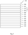
- Fig. 3 is a schematic sectional view of a tandem OLED 200, according to another exemplary embodiment of the present invention.
- Fig. 3 differs from Fig. 2 in that the OLED 100 of Fig. 3 further comprises a charge generation layer and a hole transport layer (HTL) 141.
- HTL hole transport layer
- the OLED 200 includes a substrate 110, an anode 120, a first hole injection layer (HIL) 130, a first hole transport layer (HTL) 140, a first electron blocking layer (EBL) 145, a first emission layer (EML) 150, a first hole blocking layer (HBL) 155, a first electron transport layer (ETL) 160, a second electron transport layer (ETL) 161, an n-type charge generation layer (n-type CGL) 185, wherein the second electron transport layer (ETL) 160 comprise compound of Formula (I) and a metal dopant, a p-type charge generation layer (p-type GCL) 135, a second hole transport layer (HTL) 141 and a cathode 190.
- the electron transport layers (ETL) 160 or the electron transport layers (ETL) 160 and the electron injection layer (EIL) 180 and/or the n-type charge generation layer (n-type CGL) 185 comprise or consist of the compound of Formula (I) and a metal dopant.
- the first hole injection layer (HIL) 130 and/or and the p-type charge generation layer (p-type GCL) 135 may comprises a radialene compound.
- Fig. 4 is a schematic sectional view of a tandem OLED 200, according to another exemplary embodiment of the present invention.
- Fig. 4 differs from Fig. 2 in that the OLED 100 of Fig. 3 further comprises a charge generation layer and a second emission layer. Referring to Fig.
- the OLED 200 includes a substrate 110, an anode 120, a first hole injection layer (HIL) 130, a first hole transport layer (HTL) 140, a first electron blocking layer (EBL) 145, a first emission layer (EML) 150, a first hole blocking layer (HBL) 155, a first electron transport layer (ETL) 160, an n-type charge generation layer (n-type CGL) 185 which may comprise compound of Formula (I) and a metal dopant, a p-type charge generation layer (p-type GCL) 135 which may comprises a radialene compound, a second hole transport layer (HTL) 141, a second electron blocking layer (EBL) 146, a second emission layer (EML) 151, a second hole blocking layer (EBL) 156, a second electron transport layer (ETL) 161, a second electron injection layer (EIL) 181 and a cathode 190.
- HIL hole injection layer
- HTL hole transport layer
- the electron transport layers (ETL) 160 and optional the electron injection layer (EIL) 180 and/or the n-type charge generation layer (n-type CGL) 185 comprise or consist of the compound of Formula (I) and a metal dopant.
- the hole injection layers (HIL) 130 and/or and the p-type charge generation layers (p-type GCL) 135 may comprises a radialene compound.
- an OLED 200 of the present invention is started with a substrate 110 onto which an anode 120 is formed, on the anode electrode 120, a first hole injection layer 130, first hole transport layer 140, optional a first electron blocking layer 145, a first emission layer 150, optional a first hole blocking layer 155, optional at least one first electron transport layer 160, an n-type CGL 185, a p-type CGL 135, a second hole transport layer 141, optional a second electron blocking layer 146, a second emission layer 151, an optional second hole blocking layer 156, an at least one second electron transport layer 161, an optional second electron injection layer (EIL) 181 and a cathode 190 are formed, in that order or the other way around.
- EIL electron injection layer
- Examples 1 to 4 and comparative examples 1 to 2 a glass substrate was cut to a size of 150 mm x 150 mm x 0.7 mm, ultrasonically cleaned with isopropyl alcohol for 5 minutes and then with pure water for 5 minutes, and cleaned again with UV ozone for 30 minutes, to prepare a first electrode. 90 nm ITO were deposited on the glass substrate at a pressure of 10 -5 to 10 -7 mbar to form the anode.
- Biphenyl-4-yl(9,9-diphenyl-9H-fluoren-2-yl)-[4-(9-phenyl-9H-carbazol-3-yl) phenyl]-amine was vacuum deposited on the HIL, to form a HTL having a thickness of 128 nm.
- N,N-bis(4-(dibenzo[b,d]furan-4-yl)phenyl)-[1,1':4',1"-terphenyl]-4-amine (CAS 1198399-61-9) was vacuum deposited on the HTL, to form an electron blocking layer (EBL) having a thickness of 5 nm.
- EBL electron blocking layer
- the hole blocking layer is formed with a thickness of 5 nm by depositing 2-(3'-(9,9-dimethyl-9H-fluoren-2-yl)-[1,1'-biphenyl]-3-yl)-4,6-diphenyl-1,3,5-triazine on the emission layer.
- the electron transport layer may comprise 99 wt.-% matrix compound of Formula 1 and 1 wt.-% of Li as metal dopant or electron transport layer may comprise 97 wt.-% matrix compound of Formula 1 and 3 wt.-% of Yb, see Table 3.
- Al is evaporated at a rate of 0.01 to 1 A/s at 10 -7 mbar to form a cathode with a thickness of 100 nm.
- the OLED stack is protected from ambient conditions by encapsulation of the device with a glass slide. Thereby, a cavity is formed, which includes a getter material for further protection.
- Examples 5 to 10 and comparative examples 3 to 5 a glass substrate was cut to a size of 150 mm x 150 mm x 0.7 mm, ultrasonically cleaned with isopropyl alcohol for 5 minutes and then with pure water for 5 minutes, and cleaned again with UV ozone for 30 minutes, to prepare a first electrode. 90 nm ITO were deposited on the glass substrate at a pressure of 10 -5 to 10 -7 mbar to form the anode.
- Biphenyl-4-yl(9,9-diphenyl-9H-fluoren-2-yl)-[4-(9-phenyl-9H-carbazol-3-yl) phenyl]-amine was vacuum deposited on the HIL, to form a first HTL having a thickness of 128 nm.
- N,N-bis(4-(dibenzo[b,d]furan-4-yl)phenyl)-[1,1':4',1"-terphenyl]-4-amine (CAS 1198399-61-9) was vacuum deposited on the HTL, to form an electron blocking layer (EBL) having a thickness of 5 nm.
- EBL electron blocking layer
- the first hole blocking layer is formed with a thickness of 5 nm by depositing 2-(3'-(9,9-dimethyl-9H-fluoren-2-yl)-[1,1'-biphenyl]-3-yl)-4,6-diphenyl-1,3,5-triazine on the emission layer.
- the electron transporting layer having a thickness of 25 nm is formed on the hole blocking layer by depositing 4'-(4-(4-(4,6-diphenyl-1,3,5-triazin-2-yl)phenyl)naphthalen-1-yl)-[1,1'-biphenyl]-4-carbonitrile.
- the electron transport layer (ETL) comprises 50 wt.-% matrix compound and 50 wt.-% of LiQ.
- the n-CGL comprises 99 wt.-% matrix compound of Formula 1 and 1 wt.-% of Li as metal dopant or electron transport layer may comprise 97 wt.-% matrix compound of Formula 1 and 3 wt.-% of Yb, see Table 4.
- the p-CGL was formed on n-CGL with a thickness of 10 nm on n-CGL by depositing Biphenyl-4-yl(9,9-diphenyl-9H-fluoren-2-yl)-[4-(9-phenyl-9H-carbazol-3-yl)phenyl]-amine (CAS 1242056-42-3) with 2,2',2"-(cyclopropane-1,2,3-triylidene)tris(2-(p-cyanotetrafluorophenyl)acetonitrile) (A2) according the inventive example 5-10.
- Table 4 Table 4
- p-CGL was formed on n-CGL in the same way as in inventive examples accept that HAT-CN was used instead of A2.
- Biphenyl-4-yl(9,9-diphenyl-9H-fluoren-2-yl)-[4-(9-phenyl-9H-carbazol-3-yl) phenyl]-amine was vacuum deposited on the p-CGL, to form a second HTL having a thickness of 10 nm.
- Al is evaporated at a rate of 0.01 to 1 A/s at 10 -7 mbar to form a cathode with a thickness of 100 nm.
- the OLED stack is protected from ambient conditions by encapsulation of the device with a glass slide. Thereby, a cavity is formed, which includes a getter material for further protection.
- the current efficiency is measured at 20°C.
- the current-voltage characteristic is determined using a Keithley 2635 source measure unit, by sourcing a voltage in V and measuring the current in mA flowing through the device under test. The voltage applied to the device is varied in steps of 0.1V in the range between 0V and 10V.
- the luminance-voltage characteristics and CIE coordinates are determined by measuring the luminance in cd/m 2 using an Instrument Systems CAS-140CT array spectrometer (calibrated by Deutsche Ak relie für sstelle (DAkkS)) for each of the voltage values.
- the cd/A efficiency at 10 mA/cm 2 is determined by interpolating the luminance-voltage and current-voltage characteristics, respectively.
- Lifetime LT of the device is measured at ambient conditions (20°C) and 30 mA/cm 2 , using a Keithley 2400 source meter, and recorded in hours.
- the brightness of the device is measured using a calibrated photo diode.
- the lifetime LT is defined as the time till the brightness of the device is reduced to 97 % of its initial value.
- Example 1-4 the material for ETL (Example 1-4) and n-CGL (Example 5-8) can secure low driving voltage and high efficiency of an organic electronic device, when used in an organic electronic device.
- Table 3 Performance of an OLED device comprising an electron transport layer 2 comprising a compound of formula 1 and a metal dopant Example Table 3 Operating voltage at 10 mA/cm 2 (V) HIL ETL Matrix compound Matrix compound conc. (vol.-%) Dopant Dopant conc. (vol.-%) Matrix compound Matrix compound conc. (vol.-%) Dopant Dopant conc.
- Example 1 (Comparative -- -- HAT-CN 100 G1 97 Yb 3 5.5
- Example 2 (Comparative) -- -- HAT-CN 100 G12 97 Yb 3 5.7
- Example 1 HTM-1 97 A2 3 G1 99 Li 1 4.7
- Example 2 HTM-1 97 A2 3 G1 97 Yb 3 4.6
- Example 3 HTM-1 97 A2 3 G12 99 Li 1 3.8
- Table 3 shows that the OLED device containing ETL comprising compound of Formula (I) and a metal dopant and HIL comprising of a HTM-1 and A2 as dopant have lower operating voltage (cd/A at 15 mA/cm 2 ) as compared to the OLED device containing ETL comprising of compound of formula 1 and a metal dopant and HIL comprising HAT-CN.
- Table 4 Performance of an organic electronic device comprising an n-CGL comprising a compound of Formula (I) and a metal dopant
- Example Table 4 cd/A efficiency at 15 mA/cm 2 (cd/A) p-CGL nCGL Operating voltage at 15 mA/cm 2 (V) Matrix compound Matrix compound conc. (vol.-%) Dopant Dopant conc. (vol.-%) Matrix compound Matrix compound conc. (vol.-%) Dopant Dopant conc.
- Example 3 (comparative) HTM-1 90 HAT-CN 10 G36 99 Li 1 9.2 6.8
- Example 4 (comparative) HTM-1 90 HAT-CN 10 G36 97 Yb 3 8.7 6.5
- Example 5 HTM-1 90 A2 10 G36 99 Li 1 5.2 6.8
- Example 6 HTM-1 90 A2 10 G36 97 Yb 3 5.1 6.6
- Example 7 HTM-1 90 A2 10 G1 99 Li 1 5.2 6.8
- Example 8 HTM-1 90 A2 10 G1 97 Yb 3 5.1 6.7
- Example 9 HTM-1 90 A2 10 G12 99 Li 1 5.2 6.8
- Example 10 HTM-1 90 A2 10 G12 97 Yb 3 5.1 6.9
- Table 4 shows that the OLED device containing n-CGL comprising compound of Formula (1) and a metal dopant and p-CGL comprising an HTM-1 and A2 have lower operating voltage (cd/A at 15 mA/cm 2 ) as compared to the OLED device containing n-CGL comprising compound of formula 1 and a metal dopant and comprising p-CGL comprising of compound of HTM-1 and HAT-CN.
- low operating voltage (cd/A at 15 mA/cm 2 ) and improved lifetime may be achieved when the first organic semiconductor layer may comprise a compound of Formula (I) and metal dopant.
Landscapes
- Chemical & Material Sciences (AREA)
- Physics & Mathematics (AREA)
- Engineering & Computer Science (AREA)
- Materials Engineering (AREA)
- Spectroscopy & Molecular Physics (AREA)
- Organic Chemistry (AREA)
- Optics & Photonics (AREA)
- Electroluminescent Light Sources (AREA)
Claims (15)
- Dispositif électronique organique comprenant une anode, une première couche de semi-conducteur organique, une deuxième couche de semi-conducteur organique et une cathode ;a) la première couche de semi-conducteur organique comprenant :un dopant métallique, etun composé de formule (I) :
 Ar1 et Ar2 étant identiques ou différents et indépendamment choisis parmi hydrogène, C6 à C36 aryle substitué ou non substitué, C3 à C36 hétéroaryle substitué ou non substitué, au moins l'un parmi le groupe Ar1 et Ar2 comprenant un C3 à C36 hétéroaryle substitué ou non substitué ;L étant une simple liaison, un C6 à C18 arylène substitué ou non substitué, un C3 à C18 hétéroarylène substitué ou non substitué, un phénylène substitué ou non substitué, un biphénylène substitué ou non substitué, un terphénylène substitué ou non substitué, un anthracénylène substitué ou non substitué, un dibenzofuranylène substitué ou non substitué, un dibenzothiophénylène substitué ou non substitué, un carbazolylène substitué ou non substitué, un pyridinylène substitué ou non substitué, un phénylpyridinylène substitué ou non substitué, un quinoléinylène substitué ou non substitué ;Ar3 étant un groupe choisi parmi un C6 à C36 aryle substitué ou non substitué, C6 à C36 arylène substitué ou non substitué, un groupe C3 à C36 hétéroaryle substitué ou non substitué, un groupe C3 à C36 hétéroarylène substitué ou non substitué, un pyrazinylène substitué, un pyrimidinylène substitué, un acridinylène substitué ou non substitué, un benzoacridinylène substitué ou non substitué, un dibenzoacridinylène substitué ou non substitué, un dibenzofuranylène substitué ou non substitué, un carbazolylène substitué ou non substitué, un benzoquinoléinylène substitué ou non substitué, un phénanthridinylène substitué ou non substitué, un phénanthrolinylène substitué ou non substitué, un dinaphtofuranylène substitué ou non substitué, un benzo[4,5]imidazo[1,2-a]quinoléinylène substitué ou non substitué, ou un dinaphtothiophénylène substitué ou non substitué ;Ar4 étant un groupe indépendamment choisi parmi H, un C6 à C18 aryle substitué ou non substitué, un C3 à C20 hétéroaryle substitué ou non substitué, un phényle non substitué, un biphényle non substitué, un naphtyle non substitué, un anthracényle non substitué, un phénanthridinyle non substitué, un pyridinyle non substitué, un quinoléinyle non substitué, un pyrimidinyle non substitué, ou ayant la formule (II) ou (III),
 le groupe de formule (II) et (III) étant non substitué ou substitué et X2 étant choisi parmi NH, NR2, S, O ou C(R1)2 ;n étant 0, 1, 2, 3 ou 4 ;les substituants de L, Ar1, Ar2, Ar3, Ar4 et/ou N étant indépendamment choisis parmi :- H, C6 à C18 aryle, C3 à C20 hétéroaryle, C1 à C16 alkyle, C1 à C16 alcoxy, C3 à C16 alkyle ramifié, C3 à C16 alkyle cyclique, C3 à C16 alcoxy ramifié, C3 à C16 alcoxy cyclique, C1 à C16 alkyle partiellement ou perfluoré, C1 à C16 alcoxy partiellement ou perfluoré, C1 à C16 alkyle partiellement ou perdeutéré, C1 à C16 alcoxy partiellement ou perdeutéré, -PX3(R2)2, D, F ou CN ;- R1 et R2 étant indépendamment choisis parmi C6 à C12 aryle, C3 à C12 hétéroaryle, C1 à C16 alkyle, C1 à C16 alcoxy, C1 à C16 alkyle partiellement ou perfluoré, C1 à C16 alcoxy partiellement ou perfluoré, C1 à C16 alkyle partiellement ou perdeutéré, C1 à C16 alcoxy partiellement ou perdeutéré et- deux R1 pouvant être liés ensemble pour former un cycle- X3 étant choisi parmi S ou O ; etb) la deuxième couche de semi-conducteur organique comprenant au moins un composé de radialène.
 - Dispositif électronique organique selon la revendication 1, la deuxième couche de semi-conducteur organique comprenant au moins un composé de radialène, la quantité totale de groupes électroattracteurs dans le composé de radialène étant de 13 pour cent atomiques à 90 pour cent atomiques.
- Dispositif électronique organique selon la revendication 1 ou 2,- Ar1 et Ar2 étant indépendamment choisis parmi un groupe hydrogène, phényle, pyridinyle, phénylpyridinyle ou quinoléinyle ; ou- Ar1 étant hydrogène et Ar2 étant un groupe pyridinyle, phénylpyridinyle ou quinoléinyle ;- Ar1 étant phényle et Ar2 étant un groupe pyridinyle, phénylpyridinyle ou quinoléinyle ;- Ar1 étant hydrogène et Ar2 étant un groupe pyridinyle ;- Ar1 étant phényle et Ar2 étant un groupe pyridinyle ; ou- Ar1 et Ar2 étant des groupes pyridinyle.
- Dispositif électronique organique selon l'une quelconque des revendications précédentes 1 à 3,L étant un C6 à C18 arylène substitué ou non substitué, un C3 à C18 hétéroarylène substitué ou non substitué, préférablement le C6 à C18 arylène substitué ou non substitué, un C3 à C18 hétéroarylène substitué ou non substitué, qui sont choisis parmi un phénylène substitué ou non substitué, un biphénylène substitué ou non substitué, un terphénylène substitué ou non substitué, un anthracénylène substitué ou non substitué, un dibenzofuranylène substitué ou non substitué, un dibenzothiophénylène substitué ou non substitué, un carbazolylène substitué ou non substitué, un pyridinylène substitué ou non substitué, un phénylpyridinylène substitué ou non substitué, un quinoléinylène substitué ou non substitué ; ouL étant une simple liaison ; ouL étant choisi parmi un phénylène non substitué, un biphénylène non substitué, un terphénylène non substitué, un anthracénylène non substitué, un dibenzofuranylène non substitué, un dibenzothiophénylène non substitué, un pyridinylène non substitué, un phénylpyridinylène non substitué, préférablement L étant une simple liaison ou étant choisi parmi phénylène non substitué ou biphénylène non substitué.
- Dispositif électronique organique selon l'une quelconque des revendications précédentes 1 à 4,Ar3 étant un C6 à C36 aryle substitué ou non substitué, un C6 à C36 arylène substitué ou non substitué, un groupe C3 à C36 hétéroaryle substitué ou non substitué, un groupe C3 à C36 hétéroarylène substitué ou non substitué, qui sont choisis parmi un pyrazinylène substitué, un pyrimidinylène substitué, un acridinylène substitué ou non substitué, un benzoacridinylène substitué ou non substitué, un dibenzoacridinylène substitué ou non substitué, un dibenzofuranylène substitué ou non substitué, un carbazolylène substitué ou non substitué, un benzoquinoléinylène substitué ou non substitué, un phénanthridinylène substitué ou non substitué, un phénanthrolinylène substitué ou non substitué, un dinaphtofuranylène substitué ou non substitué, un benzo[4,5]imidazo[1,2-a]quinoléinylène substitué ou non substitué, ou un dinaphtothiophénylène substitué ou non substitué ; ouAr3 étant un groupe choisi parmi un pyrazinylène substitué, un benzoacridinylène substitué ou non substitué, un dibenzoacridinylène substitué ou non substitué, un benzo[4,5]imidazo[1,2-a]quinoléinylène substitué ou non substitué.
- Dispositif électronique organique selon l'une quelconque des revendications précédentes 1 à 5,- Ar4 étant H, ou un C6 à C18 aryle substitué ou non substitué, un C3 à C20 hétéroaryle substitué ou non substitué, qui sont choisis parmi un phényle non substitué, un biphényle non substitué, un naphtyle non substitué, un anthracényle non substitué, un phénanthridinyle non substitué, un pyridinyle non substitué, un quinoléinyle non substitué, un pyrimidinyle non substitué, ou un groupe ayant la formule (II) ou (III) ;- Ar4 étant un groupe choisi parmi H, un phényle non substitué, un biphényle non substitué, un pyridinyle non substitué, un naphtyle non substitué, un dibenzofuranyle non substitué, un benzofuranyle non substitué, un dibenzothiophényle non substitué, un benzothiophényle non substitué ; ou- H.
- Dispositif électronique organique selon l'une quelconque des revendications précédentes 1 à 6, le composé de radialène étant un [3]-radialène et étant choisi parmi A1 à A21 :
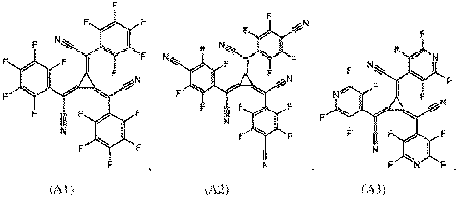

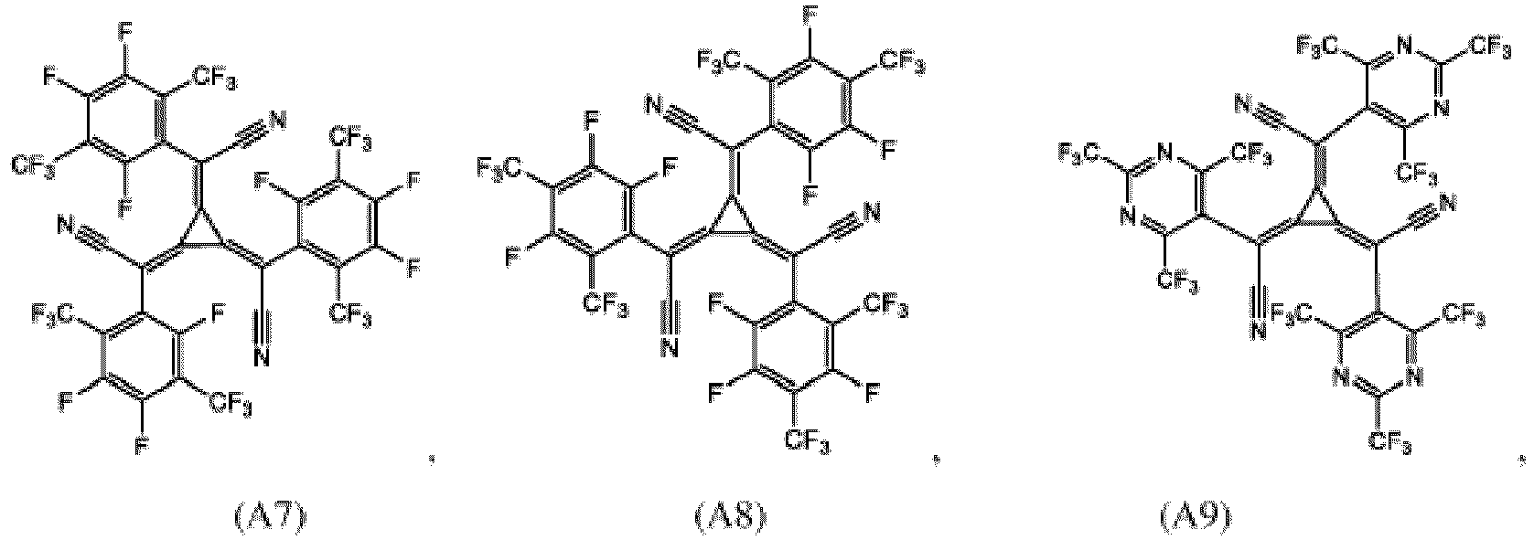


- Dispositif électronique organique selon l'une quelconque des revendications précédentes 1 à 7, le dopant métallique étant :- un métal choisi dans le groupe constitué par des métaux alcalins, des métaux alcalino-terreux et des métaux des terres rares ;- un métal choisi parmi Li, Na, Cs, Mg, Ca, Sr, Sm ou Yb ;- un métal choisi parmi Li, Cs, Mg ou Yb ; ou- un métal choisi parmi Li ou Yb.
- Dispositif électronique organique selon l'une quelconque des revendications précédentes 1 à 8, L étant indépendamment choisi parmi B1 à B21 :


- Dispositif électronique organique selon l'une quelconque des revendications précédentes 1 à 9, Ar3 étant indépendamment choisi parmi E1 à E9 :
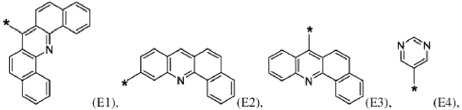

- Dispositif électronique organique selon l'une quelconque des revendications précédentes 1 à 10, Ar4 étant indépendamment choisi parmi hydrogène ou F1 à F13 :




- Dispositif électronique organique selon l'une quelconque des revendications précédentes 1 à 11, le composé de formule(I) étant choisi parmi G1 à G53 :
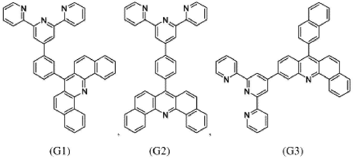


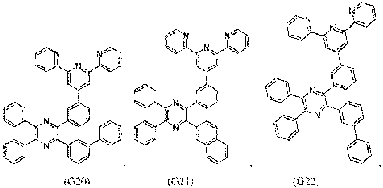


- Dispositif électronique organique selon l'une quelconque des revendications précédentes 1 à 12, le dispositif électronique organique comprenant en outre au moins une couche d'émission et la première couche de semi-conducteur organique étant agencée entre l'au moins une couche d'émission et la cathode et la deuxième couche de semi-conducteur organique étant agencée entre l'au moins une couche d'émission et l'anode.
- Dispositif électronique organique selon les revendications 1 à 13, le dispositif électronique étant un dispositif émetteur de lumière, un transistor en film mince, une batterie, un dispositif d'affichage ou une cellule photovoltaïque, et préférablement un dispositif émetteur de lumière.
- Composé représenté par la formule suivante (I) :
 Ar1 et Ar2 étant identiques ou différents et indépendamment choisis parmi hydrogène, C6 à C36 aryle substitué ou non substitué, C3 à C36 hétéroaryle substitué ou non substitué, au moins l'un parmi le groupe Ar1 et Ar2 comprenant un C3 à C36 hétéroaryle substitué ou non substitué ; Ar1 et/ou Ar2 étant lié(s) au cycle pyridinyle de formule (I) via un atome de carbone ou via un atome de N si les atomes de carbone sont tous substitués ;L étant une simple liaison, ou L étant un C6 à C24 arylène substitué ou non substitué, un C3 à C20 hétéroarylène substitué ou non substitué, un phénylène substitué ou non substitué, un biphénylène substitué ou non substitué, un terphénylène substitué ou non substitué, un naphtalénylène substitué ou non substitué, un anthracénylène substitué ou non substitué, dibenzofuranylène, dibenzothiophénylène, carbazolylène, pyridinylène, phénylpyridinylène, quinoléinylène ;Ar3 étant un groupe choisi parmi benzo[4,5]imidazo[1,2-a]quinoléinylène substitué ou non substitué ou benzo[4,5]imidazo[1,2-a]quinoléinyle substitué ou non substitué ;Ar4 étant un groupe indépendamment choisi parmi H, C6 à C18 aryle substitué ou non substitué, C3 à C20 hétéroaryle substitué ou non substitué, phényle non substitué, biphényle non substitué, naphtyle non substitué, anthracényle non substitué, phénanthridinylène non substitué, pyridinyle non substitué, quinoléinyle non substitué, pyrimidinyle non substitué, ou ayant la formule (II) ou (III),
 le groupe de formule (II) et (III) étant substitué ou non substitué et X2 étant choisi parmi NH, NR2, S, O ou CR1 ; n étant 0, 1, 2, 3 ou 4 ;les substituants de L, Ar1, Ar2, Ar3, Ar4 et/ou N s'ils ne sont pas liés à des groupes adjacents étant indépendamment choisis parmi :- H, ou C6 à C18 aryle, C3 à C20 hétéroaryle, C1 à C16 alkyle, C1 à C16 alcoxy, C3 à C16 alkyle ramifié, C3 à C16 alkyle cyclique, C3 à C16 alcoxy ramifié, C3 à C16 alcoxy cyclique, C1 à C16 alkyle partiellement ou perfluoré, C1 à C16 alcoxy partiellement ou perfluoré, C1 à C16 alkyle partiellement ou perdeutéré, C1 à C16 alcoxy partiellement ou perdeutéré, -PX2(R2)2, D, F ou CN ;- R2 étant indépendamment choisi parmi C6 à C12 aryle, C3 à C12 hétéroaryle, C1 à C16 alkyle, C1 à C16 alcoxy, C1 à C16 alkyle partiellement ou perfluoré, C1 à C16 alcoxy partiellement ou perfluoré, C1 à C16 alkyle partiellement ou perdeutéré, C1 à C16 alcoxy partiellement ou perdeutéré et- X2 étant choisi parmi S et O.
Applications Claiming Priority (2)
| Application Number | Priority Date | Filing Date | Title |
|---|---|---|---|
| EP19199928.3A EP3799143B1 (fr) | 2019-09-26 | 2019-09-26 | Première et seconde couches semiconductrices organiques et dispositif électronique organique les comprenant |
| PCT/EP2020/076945 WO2021058761A1 (fr) | 2019-09-26 | 2020-09-25 | Première et seconde couches semi-conductrices organiques et dispositif électronique organique les comprenant |
Publications (2)
| Publication Number | Publication Date |
|---|---|
| EP4035217A1 EP4035217A1 (fr) | 2022-08-03 |
| EP4035217B1 true EP4035217B1 (fr) | 2024-09-11 |
Family
ID=68290144
Family Applications (2)
| Application Number | Title | Priority Date | Filing Date |
|---|---|---|---|
| EP19199928.3A Active EP3799143B1 (fr) | 2019-09-26 | 2019-09-26 | Première et seconde couches semiconductrices organiques et dispositif électronique organique les comprenant |
| EP20775354.2A Active EP4035217B1 (fr) | 2019-09-26 | 2020-09-25 | Première et seconde couches semiconductrices organiques et dispositif électronique organique les comprenant |
Family Applications Before (1)
| Application Number | Title | Priority Date | Filing Date |
|---|---|---|---|
| EP19199928.3A Active EP3799143B1 (fr) | 2019-09-26 | 2019-09-26 | Première et seconde couches semiconductrices organiques et dispositif électronique organique les comprenant |
Country Status (5)
| Country | Link |
|---|---|
| US (1) | US20230240136A1 (fr) |
| EP (2) | EP3799143B1 (fr) |
| KR (1) | KR20220069959A (fr) |
| CN (1) | CN114503297B (fr) |
| WO (1) | WO2021058761A1 (fr) |
Families Citing this family (9)
| Publication number | Priority date | Publication date | Assignee | Title |
|---|---|---|---|---|
| EP3989303A1 (fr) * | 2020-10-22 | 2022-04-27 | Novaled GmbH | Composé organique de formule (i) à utiliser dans des dispositifs électroniques organiques, dispositif électronique organique comprenant un composé de formule (i) et dispositif d'affichage comprenant le dispositif électronique organique |
| EP4113639B1 (fr) * | 2021-06-29 | 2025-02-26 | Novaled GmbH | Composé organique de formule (i) pour une utilisation dans des dispositifs électroniques organiques, dispositif électronique organique comprenant un composé de formule (i) et dispositif d'affichage comprenant le dispositif électronique organique |
| EP4199125A1 (fr) | 2021-12-14 | 2023-06-21 | Novaled GmbH | Diode électroluminescente organique, son procédé de préparation et dispositif la comprenant |
| EP4198103A1 (fr) | 2021-12-14 | 2023-06-21 | Novaled GmbH | Diode électroluminescente organique et dispositif le comprenant |
| EP4199096B1 (fr) | 2021-12-20 | 2024-03-27 | Novaled GmbH | Dispositif d'affichage comprenant une couche de génération de charge commune et son procédé de fabrication |
| EP4199132A1 (fr) * | 2021-12-20 | 2023-06-21 | Novaled GmbH | Couche de génération de charge comprenant un composé de formule (i), dispositif électronique organique et dispositif d'affichage comprenant la couche de génération de charge ainsi que composés de formule (i) |
| EP4273948A1 (fr) | 2022-05-02 | 2023-11-08 | Novaled GmbH | Diode électroluminescente organique et dispositif le comprenant |
| KR20250136312A (ko) * | 2022-12-16 | 2025-09-16 | 노발레드 게엠베하 | 화학식 (i)의 화합물 및 화학식 (ia)의 화합물을 포함하는 유기 전자 장치 및 디스플레이 장치 |
| EP4482280A1 (fr) * | 2023-06-19 | 2024-12-25 | Novaled GmbH | Composition comprenant un composé de formule (iv) et au moins un composé de formule (iv) |
Citations (1)
| Publication number | Priority date | Publication date | Assignee | Title |
|---|---|---|---|---|
| EP2311826A2 (fr) * | 2008-11-03 | 2011-04-20 | LG Chem, Ltd. | Nouveau composé hétérocyclique contenant de l'azote et dispositif électronique organique utilisant un tel composé |
Family Cites Families (16)
| Publication number | Priority date | Publication date | Assignee | Title |
|---|---|---|---|---|
| US6140763A (en) | 1998-07-28 | 2000-10-31 | Eastman Kodak Company | Interfacial electron-injecting layer formed from a doped cathode for organic light-emitting structure |
| KR100329571B1 (ko) | 2000-03-27 | 2002-03-23 | 김순택 | 유기 전자 발광소자 |
| EP1486551B1 (fr) * | 2003-06-13 | 2016-03-16 | Semiconductor Energy Laboratory Co., Ltd. | Elément luminescent et dispositif luminescent |
| KR101398711B1 (ko) * | 2009-02-27 | 2014-05-27 | 주식회사 엘지화학 | 질소 함유 복소환 화합물 및 이를 이용한 유기전자소자 |
| KR101561730B1 (ko) * | 2012-02-06 | 2015-10-22 | 주식회사 엘지화학 | 질소원소를 함유한 헤테로고리 유도체 및 이를 이용한 유기 전자 소자 |
| KR102164046B1 (ko) * | 2013-12-03 | 2020-10-12 | 덕산네오룩스 주식회사 | 유기전기 소자용 화합물, 이를 이용한 유기전기소자 및 그 전자 장치 |
| CN107207503A (zh) * | 2015-01-29 | 2017-09-26 | 东丽株式会社 | 菲咯啉衍生物、含有其的电子装置、发光元件及光电转换元件 |
| KR102321381B1 (ko) | 2015-02-23 | 2021-11-04 | 삼성디스플레이 주식회사 | 유기 발광 소자 |
| KR20170003471A (ko) * | 2015-06-30 | 2017-01-09 | (주)피엔에이치테크 | 유기발광 화합물 및 이를 포함하는 유기전계발광소자 |
| EP3252837B1 (fr) * | 2016-05-30 | 2021-05-05 | Novaled GmbH | Diode électroluminescente organique comprenant une couche semi-conductrice organique |
| US9929360B2 (en) * | 2016-07-08 | 2018-03-27 | Universal Display Corporation | Organic electroluminescent materials and devices |
| EP3369729B1 (fr) * | 2017-03-02 | 2022-01-12 | Novaled GmbH | Dérivés de 9-phényl-acridine condensés à utiliser dans un dispositif électronique et dispositif d'affichage |
| KR102331322B1 (ko) * | 2017-03-08 | 2021-11-24 | 주식회사 엘지화학 | 유기 발광 소자 |
| CN107805248A (zh) * | 2017-11-01 | 2018-03-16 | 长春海谱润斯科技有限公司 | 一种含有苯并咪唑结构的衍生物及其制备方法和有机电致发光器件 |
| CN109206420B (zh) * | 2017-12-14 | 2022-08-02 | 江苏三月科技股份有限公司 | 一种基于三嗪的有机化合物及其在有机电致发光器件上的应用 |
| CN109560207A (zh) * | 2018-12-11 | 2019-04-02 | 长春海谱润斯科技有限公司 | 一种有机材料及其有机电致发光器件 |
-
2019
- 2019-09-26 EP EP19199928.3A patent/EP3799143B1/fr active Active
-
2020
- 2020-09-24 US US17/764,147 patent/US20230240136A1/en active Pending
- 2020-09-25 WO PCT/EP2020/076945 patent/WO2021058761A1/fr not_active Ceased
- 2020-09-25 CN CN202080066558.3A patent/CN114503297B/zh active Active
- 2020-09-25 EP EP20775354.2A patent/EP4035217B1/fr active Active
- 2020-09-25 KR KR1020227011918A patent/KR20220069959A/ko not_active Ceased
Patent Citations (1)
| Publication number | Priority date | Publication date | Assignee | Title |
|---|---|---|---|---|
| EP2311826A2 (fr) * | 2008-11-03 | 2011-04-20 | LG Chem, Ltd. | Nouveau composé hétérocyclique contenant de l'azote et dispositif électronique organique utilisant un tel composé |
Also Published As
| Publication number | Publication date |
|---|---|
| CN114503297A (zh) | 2022-05-13 |
| KR20220069959A (ko) | 2022-05-27 |
| CN114503297B (zh) | 2025-12-09 |
| EP4035217A1 (fr) | 2022-08-03 |
| EP3799143A1 (fr) | 2021-03-31 |
| US20230240136A1 (en) | 2023-07-27 |
| WO2021058761A1 (fr) | 2021-04-01 |
| EP3799143B1 (fr) | 2024-09-11 |
Similar Documents
| Publication | Publication Date | Title |
|---|---|---|
| EP4035217B1 (fr) | Première et seconde couches semiconductrices organiques et dispositif électronique organique les comprenant | |
| EP3824500B1 (fr) | Composé et couche semiconductrice organique, dispositif électronique organique, dispositif d'affichage et dispositif d'éclairage le comprenant | |
| EP3407401A1 (fr) | Dispositif électronique organique comprenant une couche semi-conductrice organique et un dispositif | |
| EP3470398B1 (fr) | Dispositif électronique organique comprenant une couche semi-conductrice organique | |
| EP3502106B1 (fr) | Composés de triazine substitués par des groupes volumineux | |
| EP3790875B1 (fr) | Composés n-hétéroarylène ayant de faibles énergies lumo | |
| EP3470412B1 (fr) | Dispositif électronique organique comprenant une couche semi-conductrice organique | |
| EP3406599A1 (fr) | Dispositif électronique organique comprenant une couche organique semi-conductrice | |
| EP3835295A1 (fr) | Composé acridine et couche semiconductrice organique, dispositif électronique organique et dispositif d'affichage le comprenant | |
| EP3840081A1 (fr) | Dispositif électronique organique comprenant un composé de formule (1), dispositif d'affichage comprenant le dispositif électronique organique ainsi que composés de formule (1) pour une utilisation dans des dispositifs électroniques organiques | |
| EP3312171B1 (fr) | Composé pour dispositif électronique et dispositif d'affichage et dispositif électronique | |
| EP3589617B1 (fr) | Composé d'acridine destiné à être utilisé dans un dispositif électronique et dispositif d'affichage | |
| EP3840075A1 (fr) | Dispositif électronique organique comprenant un composé de formule (1), dispositif d'affichage comprenant le dispositif électronique organique ainsi que composés de formule (1) pour une utilisation dans des dispositifs électroniques organiques | |
| EP3757100B1 (fr) | Composés de triazine substitués par des groupes volumineux | |
| EP3840080A1 (fr) | Dispositif électronique organique et dispositif d'affichage comprenant le dispositif électronique organique | |
| EP3798213B1 (fr) | Couche semi-conductrice organique, dispositif électronique organique la comprenant et composés correspondants | |
| EP3527557A1 (fr) | Composés n-hétéroarylène | |
| EP3483153B1 (fr) | Composés comprenant du groups triazine, fluorene et aryle et leur application en dispositifs électroniques organiques | |
| EP4356445B1 (fr) | Dispositif électronique organique comprenant un substrat, une couche d'anode, une couche de cathode, au moins une première couche d'émission et au moins une couche d'injection de trous qui comprend un complexe métallique | |
| EP3643720B1 (fr) | Composés organiques, couche semi-conductrice organique et dispositif électronique organique | |
| US20220231234A1 (en) | Compounds comprising a hetero-fluorene group | |
| EP3483154A1 (fr) | Composés comprenant du groups triazine, fluorene et aryle et leur application en dispositifs électroniques organiques |
Legal Events
| Date | Code | Title | Description |
|---|---|---|---|
| STAA | Information on the status of an ep patent application or granted ep patent |
Free format text: STATUS: UNKNOWN |
|
| STAA | Information on the status of an ep patent application or granted ep patent |
Free format text: STATUS: THE INTERNATIONAL PUBLICATION HAS BEEN MADE |
|
| PUAI | Public reference made under article 153(3) epc to a published international application that has entered the european phase |
Free format text: ORIGINAL CODE: 0009012 |
|
| STAA | Information on the status of an ep patent application or granted ep patent |
Free format text: STATUS: REQUEST FOR EXAMINATION WAS MADE |
|
| 17P | Request for examination filed |
Effective date: 20220328 |
|
| AK | Designated contracting states |
Kind code of ref document: A1 Designated state(s): AL AT BE BG CH CY CZ DE DK EE ES FI FR GB GR HR HU IE IS IT LI LT LU LV MC MK MT NL NO PL PT RO RS SE SI SK SM TR |
|
| DAV | Request for validation of the european patent (deleted) | ||
| DAX | Request for extension of the european patent (deleted) | ||
| REG | Reference to a national code |
Ref country code: DE Ref legal event code: R079 Free format text: PREVIOUS MAIN CLASS: H01L0051540000 Ipc: H10K0085600000 Ref document number: 602020037605 Country of ref document: DE |
|
| RIC1 | Information provided on ipc code assigned before grant |
Ipc: H10K 50/19 20230101ALN20240308BHEP Ipc: H10K 50/17 20230101ALN20240308BHEP Ipc: H10K 50/165 20230101ALN20240308BHEP Ipc: H10K 50/155 20230101ALN20240308BHEP Ipc: H10K 85/60 20230101AFI20240308BHEP |
|
| GRAP | Despatch of communication of intention to grant a patent |
Free format text: ORIGINAL CODE: EPIDOSNIGR1 |
|
| STAA | Information on the status of an ep patent application or granted ep patent |
Free format text: STATUS: GRANT OF PATENT IS INTENDED |
|
| INTG | Intention to grant announced |
Effective date: 20240419 |
|
| GRAS | Grant fee paid |
Free format text: ORIGINAL CODE: EPIDOSNIGR3 |
|
| P01 | Opt-out of the competence of the unified patent court (upc) registered |
Free format text: CASE NUMBER: APP_39533/2024 Effective date: 20240703 |
|
| GRAA | (expected) grant |
Free format text: ORIGINAL CODE: 0009210 |
|
| STAA | Information on the status of an ep patent application or granted ep patent |
Free format text: STATUS: THE PATENT HAS BEEN GRANTED |
|
| AK | Designated contracting states |
Kind code of ref document: B1 Designated state(s): AL AT BE BG CH CY CZ DE DK EE ES FI FR GB GR HR HU IE IS IT LI LT LU LV MC MK MT NL NO PL PT RO RS SE SI SK SM TR |
|
| REG | Reference to a national code |
Ref country code: GB Ref legal event code: FG4D |
|
| REG | Reference to a national code |
Ref country code: CH Ref legal event code: EP |
|
| REG | Reference to a national code |
Ref country code: DE Ref legal event code: R096 Ref document number: 602020037605 Country of ref document: DE |
|
| REG | Reference to a national code |
Ref country code: IE Ref legal event code: FG4D |
|
| REG | Reference to a national code |
Ref country code: LT Ref legal event code: MG9D |
|
| PG25 | Lapsed in a contracting state [announced via postgrant information from national office to epo] |
Ref country code: NO Free format text: LAPSE BECAUSE OF FAILURE TO SUBMIT A TRANSLATION OF THE DESCRIPTION OR TO PAY THE FEE WITHIN THE PRESCRIBED TIME-LIMIT Effective date: 20241211 |
|
| REG | Reference to a national code |
Ref country code: NL Ref legal event code: MP Effective date: 20240911 |
|
| PG25 | Lapsed in a contracting state [announced via postgrant information from national office to epo] |
Ref country code: GR Free format text: LAPSE BECAUSE OF FAILURE TO SUBMIT A TRANSLATION OF THE DESCRIPTION OR TO PAY THE FEE WITHIN THE PRESCRIBED TIME-LIMIT Effective date: 20241212 Ref country code: FI Free format text: LAPSE BECAUSE OF FAILURE TO SUBMIT A TRANSLATION OF THE DESCRIPTION OR TO PAY THE FEE WITHIN THE PRESCRIBED TIME-LIMIT Effective date: 20240911 |
|
| PG25 | Lapsed in a contracting state [announced via postgrant information from national office to epo] |
Ref country code: BG Free format text: LAPSE BECAUSE OF FAILURE TO SUBMIT A TRANSLATION OF THE DESCRIPTION OR TO PAY THE FEE WITHIN THE PRESCRIBED TIME-LIMIT Effective date: 20240911 |
|
| PG25 | Lapsed in a contracting state [announced via postgrant information from national office to epo] |
Ref country code: LV Free format text: LAPSE BECAUSE OF FAILURE TO SUBMIT A TRANSLATION OF THE DESCRIPTION OR TO PAY THE FEE WITHIN THE PRESCRIBED TIME-LIMIT Effective date: 20240911 |
|
| PG25 | Lapsed in a contracting state [announced via postgrant information from national office to epo] |
Ref country code: HR Free format text: LAPSE BECAUSE OF FAILURE TO SUBMIT A TRANSLATION OF THE DESCRIPTION OR TO PAY THE FEE WITHIN THE PRESCRIBED TIME-LIMIT Effective date: 20240911 |
|
| PG25 | Lapsed in a contracting state [announced via postgrant information from national office to epo] |
Ref country code: RS Free format text: LAPSE BECAUSE OF FAILURE TO SUBMIT A TRANSLATION OF THE DESCRIPTION OR TO PAY THE FEE WITHIN THE PRESCRIBED TIME-LIMIT Effective date: 20241211 Ref country code: ES Free format text: LAPSE BECAUSE OF FAILURE TO SUBMIT A TRANSLATION OF THE DESCRIPTION OR TO PAY THE FEE WITHIN THE PRESCRIBED TIME-LIMIT Effective date: 20240911 |
|
| PG25 | Lapsed in a contracting state [announced via postgrant information from national office to epo] |
Ref country code: RS Free format text: LAPSE BECAUSE OF FAILURE TO SUBMIT A TRANSLATION OF THE DESCRIPTION OR TO PAY THE FEE WITHIN THE PRESCRIBED TIME-LIMIT Effective date: 20241211 Ref country code: NO Free format text: LAPSE BECAUSE OF FAILURE TO SUBMIT A TRANSLATION OF THE DESCRIPTION OR TO PAY THE FEE WITHIN THE PRESCRIBED TIME-LIMIT Effective date: 20241211 Ref country code: LV Free format text: LAPSE BECAUSE OF FAILURE TO SUBMIT A TRANSLATION OF THE DESCRIPTION OR TO PAY THE FEE WITHIN THE PRESCRIBED TIME-LIMIT Effective date: 20240911 Ref country code: HR Free format text: LAPSE BECAUSE OF FAILURE TO SUBMIT A TRANSLATION OF THE DESCRIPTION OR TO PAY THE FEE WITHIN THE PRESCRIBED TIME-LIMIT Effective date: 20240911 Ref country code: GR Free format text: LAPSE BECAUSE OF FAILURE TO SUBMIT A TRANSLATION OF THE DESCRIPTION OR TO PAY THE FEE WITHIN THE PRESCRIBED TIME-LIMIT Effective date: 20241212 Ref country code: FI Free format text: LAPSE BECAUSE OF FAILURE TO SUBMIT A TRANSLATION OF THE DESCRIPTION OR TO PAY THE FEE WITHIN THE PRESCRIBED TIME-LIMIT Effective date: 20240911 Ref country code: ES Free format text: LAPSE BECAUSE OF FAILURE TO SUBMIT A TRANSLATION OF THE DESCRIPTION OR TO PAY THE FEE WITHIN THE PRESCRIBED TIME-LIMIT Effective date: 20240911 Ref country code: BG Free format text: LAPSE BECAUSE OF FAILURE TO SUBMIT A TRANSLATION OF THE DESCRIPTION OR TO PAY THE FEE WITHIN THE PRESCRIBED TIME-LIMIT Effective date: 20240911 |
|
| REG | Reference to a national code |
Ref country code: AT Ref legal event code: MK05 Ref document number: 1723849 Country of ref document: AT Kind code of ref document: T Effective date: 20240911 |
|
| PG25 | Lapsed in a contracting state [announced via postgrant information from national office to epo] |
Ref country code: NL Free format text: LAPSE BECAUSE OF FAILURE TO SUBMIT A TRANSLATION OF THE DESCRIPTION OR TO PAY THE FEE WITHIN THE PRESCRIBED TIME-LIMIT Effective date: 20240911 |
|
| PG25 | Lapsed in a contracting state [announced via postgrant information from national office to epo] |
Ref country code: PT Free format text: LAPSE BECAUSE OF FAILURE TO SUBMIT A TRANSLATION OF THE DESCRIPTION OR TO PAY THE FEE WITHIN THE PRESCRIBED TIME-LIMIT Effective date: 20250113 Ref country code: IS Free format text: LAPSE BECAUSE OF FAILURE TO SUBMIT A TRANSLATION OF THE DESCRIPTION OR TO PAY THE FEE WITHIN THE PRESCRIBED TIME-LIMIT Effective date: 20250111 |
|
| PG25 | Lapsed in a contracting state [announced via postgrant information from national office to epo] |
Ref country code: SM Free format text: LAPSE BECAUSE OF FAILURE TO SUBMIT A TRANSLATION OF THE DESCRIPTION OR TO PAY THE FEE WITHIN THE PRESCRIBED TIME-LIMIT Effective date: 20240911 Ref country code: RO Free format text: LAPSE BECAUSE OF FAILURE TO SUBMIT A TRANSLATION OF THE DESCRIPTION OR TO PAY THE FEE WITHIN THE PRESCRIBED TIME-LIMIT Effective date: 20240911 |
|
| PG25 | Lapsed in a contracting state [announced via postgrant information from national office to epo] |
Ref country code: EE Free format text: LAPSE BECAUSE OF FAILURE TO SUBMIT A TRANSLATION OF THE DESCRIPTION OR TO PAY THE FEE WITHIN THE PRESCRIBED TIME-LIMIT Effective date: 20240911 Ref country code: AT Free format text: LAPSE BECAUSE OF FAILURE TO SUBMIT A TRANSLATION OF THE DESCRIPTION OR TO PAY THE FEE WITHIN THE PRESCRIBED TIME-LIMIT Effective date: 20240911 |
|
| PG25 | Lapsed in a contracting state [announced via postgrant information from national office to epo] |
Ref country code: PL Free format text: LAPSE BECAUSE OF FAILURE TO SUBMIT A TRANSLATION OF THE DESCRIPTION OR TO PAY THE FEE WITHIN THE PRESCRIBED TIME-LIMIT Effective date: 20240911 Ref country code: CZ Free format text: LAPSE BECAUSE OF FAILURE TO SUBMIT A TRANSLATION OF THE DESCRIPTION OR TO PAY THE FEE WITHIN THE PRESCRIBED TIME-LIMIT Effective date: 20240911 |
|
| PG25 | Lapsed in a contracting state [announced via postgrant information from national office to epo] |
Ref country code: IT Free format text: LAPSE BECAUSE OF FAILURE TO SUBMIT A TRANSLATION OF THE DESCRIPTION OR TO PAY THE FEE WITHIN THE PRESCRIBED TIME-LIMIT Effective date: 20240911 Ref country code: SK Free format text: LAPSE BECAUSE OF FAILURE TO SUBMIT A TRANSLATION OF THE DESCRIPTION OR TO PAY THE FEE WITHIN THE PRESCRIBED TIME-LIMIT Effective date: 20240911 |
|
| REG | Reference to a national code |
Ref country code: CH Ref legal event code: PL |
|
| PG25 | Lapsed in a contracting state [announced via postgrant information from national office to epo] |
Ref country code: LU Free format text: LAPSE BECAUSE OF NON-PAYMENT OF DUE FEES Effective date: 20240925 |
|
| REG | Reference to a national code |
Ref country code: DE Ref legal event code: R097 Ref document number: 602020037605 Country of ref document: DE |
|
| PG25 | Lapsed in a contracting state [announced via postgrant information from national office to epo] |
Ref country code: MC Free format text: LAPSE BECAUSE OF FAILURE TO SUBMIT A TRANSLATION OF THE DESCRIPTION OR TO PAY THE FEE WITHIN THE PRESCRIBED TIME-LIMIT Effective date: 20240911 |
|
| PG25 | Lapsed in a contracting state [announced via postgrant information from national office to epo] |
Ref country code: DK Free format text: LAPSE BECAUSE OF FAILURE TO SUBMIT A TRANSLATION OF THE DESCRIPTION OR TO PAY THE FEE WITHIN THE PRESCRIBED TIME-LIMIT Effective date: 20240911 |
|
| REG | Reference to a national code |
Ref country code: BE Ref legal event code: MM Effective date: 20240930 |
|
| PG25 | Lapsed in a contracting state [announced via postgrant information from national office to epo] |
Ref country code: BE Free format text: LAPSE BECAUSE OF NON-PAYMENT OF DUE FEES Effective date: 20240930 |
|
| PLBE | No opposition filed within time limit |
Free format text: ORIGINAL CODE: 0009261 |
|
| STAA | Information on the status of an ep patent application or granted ep patent |
Free format text: STATUS: NO OPPOSITION FILED WITHIN TIME LIMIT |
|
| PG25 | Lapsed in a contracting state [announced via postgrant information from national office to epo] |
Ref country code: CH Free format text: LAPSE BECAUSE OF NON-PAYMENT OF DUE FEES Effective date: 20240930 |
|
| PG25 | Lapsed in a contracting state [announced via postgrant information from national office to epo] |
Ref country code: IE Free format text: LAPSE BECAUSE OF NON-PAYMENT OF DUE FEES Effective date: 20240925 |
|
| 26N | No opposition filed |
Effective date: 20250612 |
|
| GBPC | Gb: european patent ceased through non-payment of renewal fee |
Effective date: 20241211 |
|
| PG25 | Lapsed in a contracting state [announced via postgrant information from national office to epo] |
Ref country code: SE Free format text: LAPSE BECAUSE OF FAILURE TO SUBMIT A TRANSLATION OF THE DESCRIPTION OR TO PAY THE FEE WITHIN THE PRESCRIBED TIME-LIMIT Effective date: 20240911 |
|
| PGFP | Annual fee paid to national office [announced via postgrant information from national office to epo] |
Ref country code: DE Payment date: 20250702 Year of fee payment: 6 |
|
| PG25 | Lapsed in a contracting state [announced via postgrant information from national office to epo] |
Ref country code: GB Free format text: LAPSE BECAUSE OF NON-PAYMENT OF DUE FEES Effective date: 20241211 |
|
| PG25 | Lapsed in a contracting state [announced via postgrant information from national office to epo] |
Ref country code: FR Free format text: LAPSE BECAUSE OF NON-PAYMENT OF DUE FEES Effective date: 20241111 |
|
| PG25 | Lapsed in a contracting state [announced via postgrant information from national office to epo] |
Ref country code: CY Free format text: LAPSE BECAUSE OF FAILURE TO SUBMIT A TRANSLATION OF THE DESCRIPTION OR TO PAY THE FEE WITHIN THE PRESCRIBED TIME-LIMIT; INVALID AB INITIO Effective date: 20200925 |
|
| PG25 | Lapsed in a contracting state [announced via postgrant information from national office to epo] |
Ref country code: HU Free format text: LAPSE BECAUSE OF FAILURE TO SUBMIT A TRANSLATION OF THE DESCRIPTION OR TO PAY THE FEE WITHIN THE PRESCRIBED TIME-LIMIT; INVALID AB INITIO Effective date: 20200925 |