EP4036698A1 - Dispositif de commande tactile et son procédé de fabrication - Google Patents
Dispositif de commande tactile et son procédé de fabrication Download PDFInfo
- Publication number
- EP4036698A1 EP4036698A1 EP21163011.6A EP21163011A EP4036698A1 EP 4036698 A1 EP4036698 A1 EP 4036698A1 EP 21163011 A EP21163011 A EP 21163011A EP 4036698 A1 EP4036698 A1 EP 4036698A1
- Authority
- EP
- European Patent Office
- Prior art keywords
- transparent conductive
- metal pads
- touch device
- housing
- conductive film
- Prior art date
- Legal status (The legal status is an assumption and is not a legal conclusion. Google has not performed a legal analysis and makes no representation as to the accuracy of the status listed.)
- Withdrawn
Links
Images


Classifications
-
- G—PHYSICS
- G06—COMPUTING OR CALCULATING; COUNTING
- G06F—ELECTRIC DIGITAL DATA PROCESSING
- G06F3/00—Input arrangements for transferring data to be processed into a form capable of being handled by the computer; Output arrangements for transferring data from processing unit to output unit, e.g. interface arrangements
- G06F3/01—Input arrangements or combined input and output arrangements for interaction between user and computer
- G06F3/03—Arrangements for converting the position or the displacement of a member into a coded form
- G06F3/041—Digitisers, e.g. for touch screens or touch pads, characterised by the transducing means
- G06F3/0416—Control or interface arrangements specially adapted for digitisers
- G06F3/04164—Connections between sensors and controllers, e.g. routing lines between electrodes and connection pads
-
- G—PHYSICS
- G06—COMPUTING OR CALCULATING; COUNTING
- G06F—ELECTRIC DIGITAL DATA PROCESSING
- G06F3/00—Input arrangements for transferring data to be processed into a form capable of being handled by the computer; Output arrangements for transferring data from processing unit to output unit, e.g. interface arrangements
- G06F3/01—Input arrangements or combined input and output arrangements for interaction between user and computer
- G06F3/03—Arrangements for converting the position or the displacement of a member into a coded form
- G06F3/041—Digitisers, e.g. for touch screens or touch pads, characterised by the transducing means
- G06F3/044—Digitisers, e.g. for touch screens or touch pads, characterised by the transducing means by capacitive means
- G06F3/0445—Digitisers, e.g. for touch screens or touch pads, characterised by the transducing means by capacitive means using two or more layers of sensing electrodes, e.g. using two layers of electrodes separated by a dielectric layer
-
- G—PHYSICS
- G06—COMPUTING OR CALCULATING; COUNTING
- G06F—ELECTRIC DIGITAL DATA PROCESSING
- G06F3/00—Input arrangements for transferring data to be processed into a form capable of being handled by the computer; Output arrangements for transferring data from processing unit to output unit, e.g. interface arrangements
- G06F3/01—Input arrangements or combined input and output arrangements for interaction between user and computer
- G06F3/03—Arrangements for converting the position or the displacement of a member into a coded form
- G06F3/041—Digitisers, e.g. for touch screens or touch pads, characterised by the transducing means
- G06F3/0412—Digitisers structurally integrated in a display
-
- B—PERFORMING OPERATIONS; TRANSPORTING
- B29—WORKING OF PLASTICS; WORKING OF SUBSTANCES IN A PLASTIC STATE IN GENERAL
- B29B—PREPARATION OR PRETREATMENT OF THE MATERIAL TO BE SHAPED; MAKING GRANULES OR PREFORMS; RECOVERY OF PLASTICS OR OTHER CONSTITUENTS OF WASTE MATERIAL CONTAINING PLASTICS
- B29B11/00—Making preforms
- B29B11/06—Making preforms by moulding the material
-
- B—PERFORMING OPERATIONS; TRANSPORTING
- B29—WORKING OF PLASTICS; WORKING OF SUBSTANCES IN A PLASTIC STATE IN GENERAL
- B29C—SHAPING OR JOINING OF PLASTICS; SHAPING OF MATERIAL IN A PLASTIC STATE, NOT OTHERWISE PROVIDED FOR; AFTER-TREATMENT OF THE SHAPED PRODUCTS, e.g. REPAIRING
- B29C45/00—Injection moulding, i.e. forcing the required volume of moulding material through a nozzle into a closed mould; Apparatus therefor
- B29C45/14—Injection moulding, i.e. forcing the required volume of moulding material through a nozzle into a closed mould; Apparatus therefor incorporating preformed parts or layers, e.g. injection moulding around inserts or for coating articles
-
- G—PHYSICS
- G06—COMPUTING OR CALCULATING; COUNTING
- G06F—ELECTRIC DIGITAL DATA PROCESSING
- G06F3/00—Input arrangements for transferring data to be processed into a form capable of being handled by the computer; Output arrangements for transferring data from processing unit to output unit, e.g. interface arrangements
- G06F3/01—Input arrangements or combined input and output arrangements for interaction between user and computer
- G06F3/03—Arrangements for converting the position or the displacement of a member into a coded form
- G06F3/041—Digitisers, e.g. for touch screens or touch pads, characterised by the transducing means
- G06F3/042—Digitisers, e.g. for touch screens or touch pads, characterised by the transducing means by opto-electronic means
-
- G—PHYSICS
- G06—COMPUTING OR CALCULATING; COUNTING
- G06F—ELECTRIC DIGITAL DATA PROCESSING
- G06F3/00—Input arrangements for transferring data to be processed into a form capable of being handled by the computer; Output arrangements for transferring data from processing unit to output unit, e.g. interface arrangements
- G06F3/01—Input arrangements or combined input and output arrangements for interaction between user and computer
- G06F3/03—Arrangements for converting the position or the displacement of a member into a coded form
- G06F3/041—Digitisers, e.g. for touch screens or touch pads, characterised by the transducing means
- G06F3/047—Digitisers, e.g. for touch screens or touch pads, characterised by the transducing means using sets of wires, e.g. crossed wires
-
- B—PERFORMING OPERATIONS; TRANSPORTING
- B29—WORKING OF PLASTICS; WORKING OF SUBSTANCES IN A PLASTIC STATE IN GENERAL
- B29K—INDEXING SCHEME ASSOCIATED WITH SUBCLASSES B29B, B29C OR B29D, RELATING TO MOULDING MATERIALS OR TO MATERIALS FOR MOULDS, REINFORCEMENTS, FILLERS OR PREFORMED PARTS, e.g. INSERTS
- B29K2633/00—Use of polymers of unsaturated acids or derivatives thereof for preformed parts, e.g. for inserts
- B29K2633/04—Polymers of esters
- B29K2633/12—Polymers of methacrylic acid esters, e.g. PMMA, i.e. polymethylmethacrylate
-
- B—PERFORMING OPERATIONS; TRANSPORTING
- B29—WORKING OF PLASTICS; WORKING OF SUBSTANCES IN A PLASTIC STATE IN GENERAL
- B29K—INDEXING SCHEME ASSOCIATED WITH SUBCLASSES B29B, B29C OR B29D, RELATING TO MOULDING MATERIALS OR TO MATERIALS FOR MOULDS, REINFORCEMENTS, FILLERS OR PREFORMED PARTS, e.g. INSERTS
- B29K2669/00—Use of PC, i.e. polycarbonates or derivatives thereof for preformed parts, e.g. for inserts
-
- B—PERFORMING OPERATIONS; TRANSPORTING
- B29—WORKING OF PLASTICS; WORKING OF SUBSTANCES IN A PLASTIC STATE IN GENERAL
- B29L—INDEXING SCHEME ASSOCIATED WITH SUBCLASS B29C, RELATING TO PARTICULAR ARTICLES
- B29L2031/00—Other particular articles
- B29L2031/34—Electrical apparatus, e.g. sparking plugs or parts thereof
- B29L2031/3475—Displays, monitors, TV-sets, computer screens
-
- G—PHYSICS
- G06—COMPUTING OR CALCULATING; COUNTING
- G06F—ELECTRIC DIGITAL DATA PROCESSING
- G06F2203/00—Indexing scheme relating to G06F3/00 - G06F3/048
- G06F2203/041—Indexing scheme relating to G06F3/041 - G06F3/045
- G06F2203/04102—Flexible digitiser, i.e. constructional details for allowing the whole digitising part of a device to be flexed or rolled like a sheet of paper
-
- G—PHYSICS
- G06—COMPUTING OR CALCULATING; COUNTING
- G06F—ELECTRIC DIGITAL DATA PROCESSING
- G06F2203/00—Indexing scheme relating to G06F3/00 - G06F3/048
- G06F2203/041—Indexing scheme relating to G06F3/041 - G06F3/045
- G06F2203/04103—Manufacturing, i.e. details related to manufacturing processes specially suited for touch sensitive devices
-
- G—PHYSICS
- G06—COMPUTING OR CALCULATING; COUNTING
- G06F—ELECTRIC DIGITAL DATA PROCESSING
- G06F2203/00—Indexing scheme relating to G06F3/00 - G06F3/048
- G06F2203/041—Indexing scheme relating to G06F3/041 - G06F3/045
- G06F2203/04112—Electrode mesh in capacitive digitiser: electrode for touch sensing is formed of a mesh of very fine, normally metallic, interconnected lines that are almost invisible to see. This provides a quite large but transparent electrode surface, without need for ITO or similar transparent conductive material
Definitions
- the present invention relates to a touch device, and more particularly, to a bezel-less stereoscopic touch device and a manufacturing method thereof.
- touch devices are widely applied in various electronic devices, such as smart phones, digital cameras, tablets and other mobile electronic devices. Compared with traditional physical keys, touch devices are more convenient to use, and users can conveniently slide their fingers on the touch devices to input various operation commands.
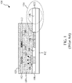
- FIG. 1 is a diagram illustrating a first exemplification of conventional touch device 100.
- the light emitting diode 104 and the touch sensor 106 are arranged on a substrate 102 and electrically connected to a circuit board (not shown in the figure) via wires 108.
- the plastic resin 110 covers the light emitting diode 104 and the touch sensor 106.
- the plastic resin 110 comprises a pattern layer which includes a shading area 112, a light leakage area 114, and pattern areas 116 and 118.
- the shading area 112 shades the light from the light emitting diode 104
- the light leakage area 114 allows the light from the light emitting diode 104 to pass through
- the pattern areas 116 and 118 can be set with patterns (e.g., patterns of numbers).
- the touch device 100 can display a pattern by the light emitting diode 104 and the pattern layer.
- the protective layer 120 covers the pattern layer.
- the touch device 100 has a tail 122 to connect to the circuit board. However, the tail 122 of the touch device 100 is prone to brittle cracking after a high temperature process. In addition, the touch device 100 needs to reserve a bezel for a wire routing area 124, which makes it impossible for the touch device 100 to achieve full-screen touch control.
- FIG. 2 is a diagram illustrating a second exemplification of conventional touch device 200.
- the touch device 200 comprises a substrate 202, a light-emitting diode 204, a touch sensor 206, a plastic resin 210, a pattern layer, and a protective layer 220.
- the light-emitting diode 204 and touch sensor 206 are disposed on the substrate 202 and are electrically connected to the circuit board 222 via the wires 208.
- the plastic resin 210 covers light-emitting diode 204 and touch sensor 206.
- the pattern layer comprises a shading area 212, a light leakage area 214, and pattern areas 216 and 218.
- the shading area 212 may shade the light from the LED 204, the light leakage area 214 allows light from the LED 204 to pass through, and the pattern areas 216 and 218 can be set with patterns (e.g., patterns of numbers).
- the touch device 200 can display a pattern by the light emitting diode 204 and the pattern layer.
- the protective layer 220 covers the pattern layer.
- the wires 208 of the touch device 200 may be connected to the circuit board 222 via a through-hole. However, if the touch device 200 first performs a wire bonding process to connect the wires 208 to the circuit board 222 and then performs a molding process, it is highly possible that the circuit board 222 may peel off.
- the touch device 200 performs the molding process and then performs the wire bonding process, the shape of the molded form would limit the wiring manner.
- the touch device 200 also needs to reserve a bezel for the wire routing area 224, in this way it is impossible for the touch device 200 to achieve full-screen touch control.
- FIG. 3 is a diagram illustrating a third exemplification of conventional touch device 300.
- a pattern layer is arranged under the substrate 302, and the pattern layer comprises a shading area 312, a light leakage area 314, and pattern areas 316 and 318.
- the shading area 312 shades the light from the light emitting diode 304
- the light leakage area 314 allows the light from the light emitting diode 304 to pass through
- the pattern areas 316 and 318 can be set with patterns (e.g. patterns of number).
- the light emitting diode 304 and the touch sensor 306 are arranged below the pattern layer and are electrically connected to a circuit board (not shown in the figure) through the wire 308 and the pin header 320.
- the plastic resin 310 covers the light emitting diode 304 and the touch sensor 306, and the substrate 302 serves as a protective layer for the touch device 300.
- the touch device 300 can display a pattern by the light emitting diode 304 and the pattern layer.
- the mold needs to avoid the pin 320 to prevent the mold from offsetting and thereby pressing the pin header 320, resulting in deformation of the pin header 320 or the glue overflow problem.
- the pin header 320 is fixed after the molding process, it is necessary to avoid the pin-pad area during the molding process and then fix the pin header 320 with conductive adhesive and epoxy resin. hence, it is more difficult to subsequent processing and rework the defective products.
- the touch device 300 also needs to reserve the bezel for the wire routing area 322, making the touch device 300 unable to achieve full-screen touch control.
- FIG. 4 is a diagram illustrating a fourth exemplification of conventional touch device 400.
- the touch device 400 comprises a substrate 402, a light emitting diode 404, a touch sensor 406, a plastic resin 410, and a pattern layer.
- the substrate 402 serves as a protective layer of the touch device 400.
- the pattern layer is arranged under the substrate 402 and comprises a shading area 412, a light leakage area 414, and pattern areas 416 and 418.
- the shading area 412 shades the light from the LED 404
- the light leakage area 414 allows the light from the LED to pass through
- the pattern areas 416 and 418 can be set with patterns (e.g., patterns of numbers).
- the light emitting diode 404 and the touch sensor 406 are located below the pattern layer and are electrically connected to a circuit board (not shown in the figure) via the wires 408 and female header 420.
- the plastic resin 410 covers the light emitting diode 404 and the touch sensor 406, and the touch device 400 can display a pattern by the light emitting diode 404 and the pattern layer.
- the touch device 400 is molded after the female header 420 is fixed, the mold needs to avoid the female header 420 to prevent the mold from offsetting and pressing the female header 420, resulting in deformation of the female header 420 or glue overflow problem.
- the touch device 400 is molded first and then fixes the female header 420, it needs to avoid the female header pad area during the molding process, and then fixes the female header 420 with conductive adhesive and epoxy resin. As a result, it would be more difficult to subsequent processing and rework the defective products.
- the touch device 400 also needs to reserve a bezel for the wire routing area 422, making the touch device 400 unable to achieve the full-screen touch control.
- the conventional touch devices 100, 200, 300 and 400 need to reserve bezels to design the wire routing area, and thus cannot achieve full-screen touch control.
- the conventional touch devices 100, 200, 300 and 400 also encounter structural and processing problems regarding the electrical connection of in-mold electronic components.
- the objective of the present invention is to propose a touch device and a manufacturing method thereof.
- the present invention provides a touch device.
- the touch device comprises a housing, a touch sensor and a circuit board.
- the housing has at least one sidewall, an inner space and an opening, wherein the at least one sidewall defines the inner space and the opening is connected to the inner space.
- the touch sensor is arranged in the inner space, and includes a substrate, a plurality of first metal pads, a sensing layer.
- the substrate is arranged on the at least one sidewall and corresponding to the shape of the housing.
- the plurality of first metal pads are arranged on the substrate.
- the sensing layer is arranged on the substrate and electrically connected to the plurality of first metal pads.
- the circuit board is arranged on the housing at a position adjacent to the opening, wherein the circuit board has a plurality of second metal pads facing towards the inner space and electrically connected to the plurality of first metal pads, respectively.
- the touch device further comprises a connector that connect the first metal pad and the second metal pad.
- the connector comprises a plurality of conductive silicone strips and a plurality of insulating silicone strips, and the plurality of conductive silicone strips are arranged interspersed with the plurality of insulating silicone strips.
- said each first metal pad or said each second metal pad is connected to at least three of the conductive silicone strips.
- the touch device further comprises a retaining frame that fixes the connector to the inner side of the housing, wherein the connector is clamped between the retaining frame and the housing.
- the touch device further comprises a display that is arranged on the retaining frame or embedded in a slot of the retaining frame.
- the touch device further comprises a lower cover that is connected to the housing and covering the opening, wherein the circuit board is fixed to the lower cover.
- the sensing layer comprises a transparent conductive film which comprises a plurality of transparent conductive wires connected to the plurality of first metal pads.
- the plurality of transparent wires are made of poly3,4-ethylenedioxythiophene or cubic boron nitride.
- the sensing layer comprises a first transparent conductive film, a second transparent conductive film and an insulating layer.
- the first transparent conductive film has a plurality of first transparent conductive wires connected to a portion of the plurality of first metal pads.
- the second transparent conductive film has a plurality of second transparent conductive wires connected to the remaining portions of the plurality of first metal pads.
- the insulating layer is between the first transparent conductive film and the second transparent conductive film.
- the plurality of first transparent wires and the plurality of second transparent wires are made of poly3,4-ethylenedioxythiophene or cubic boron nitride.
- the insulating layer is an optical adhesive.
- the substrate is made of polycarbonate or polymethyl methacrylate.
- the present invention provides a method for manufacturing a touch device, which comprises forming a plurality of first metal pads and a sensing layer on a substrate to produce a touch sensor, wherein the sensing layer is connected to the plurality of first metal pads; placing the touch sensor into a mold for thermoforming, in order to produce a three-dimensional (3D) touch sensor, wherein the plurality of first metal pads are located on the inner side of the three-dimensional touch sensor; and forming a three-dimensional housing on the outer side of the three-dimensional touch sensor by injection molding; and electrically connected to a plurality of second metal pads of a circuit board to the plurality of first metal pads, respectively.
- the step of electrically connected to the plurality of second metal pads to the plurality of first metal pads respectively comprises using a connector to connect the first metal pad and the second metal pad.
- the connector comprises a plurality of conductive silicone strips and a plurality of insulating silicone strips, and the plurality of conductive silicone strips are arranged interspersed with the plurality of insulating silicone strips.
- the method further comprises arranging said each first metal pad or said each second metal pad to connect to at least three of the conductive silicone strips.
- the method further comprises using a retaining frame to fix the connector to the inner side of the three-dimensional touch sensor, wherein the connector is connected to the plurality of first metal pads.
- the method further comprises arranging a display on the retaining frame or embedding the display in a slot of the retaining frame.
- the method further comprises combining a cover and the housing together.
- the step of forming the sensing layer comprises forming a transparent conductive film which has a plurality of transparent conductive wires connected to the plurality of first metal pads.
- the method further comprises forming the plurality of transparent conductive wires by using poly3,4-ethylenedioxythiophene or cubic boron nitride.
- the step of forming the sensing layer comprises forming a first transparent conductive film, wherein the first transparent conductive film has a plurality of first transparent conductive wires connected to a portion of the plurality of first metal pads; forming an insulating layer on the first transparent conductive film; and forming a second transparent conductive film on the insulating layer, wherein the second transparent conductive film has a plurality of second transparent conductive wires connected to the remaining portions of the plurality of first metal pads, and the insulating layer is between the first transparent conductive film and the second transparent conductive film.
- the method further comprises forming the plurality of first transparent conductive wires and the plurality of second transparent conductive wires by using poly3,4-ethylenedioxythiophene or cubic boron nitride.
- the step of forming the insulating layer comprises forming the insulating layer by using an optical adhesive.
- the method further comprises forming the substrate by using polycarbonate or polymethyl methacrylate.
- the touch device of the present invention can achieve full-screen touch control without the need for reserving a bezel to lay out wires.
- Embodiments of the present invention described below in section views and three-dimensional views are merely idealized embodiments of the invention. Therefore, differences in the shape from what is illustrated due to manufacturing processes and/or tolerances are to be expected. Hence, the embodiments of the invention should therefore not be interpreted as being limited to particular shapes of areas as illustrated in the drawings, but should also include deviations in shape resulting from manufacturing. The shapes of areas shown in the drawings are merely for illustrative purposes, rather than limitations of the scope of the present invention.
- FIG. 5 is a diagram illustrating a three-dimensional view of the touch device according to the present invention.
- FIG. 6 is a diagram illustrating a cross-sectional view of the touch device according to the present invention.
- FIG. 7 is an exploded-view diagram illustrating the touch device of the present invention.
- the touch device 500 comprises a housing 502, a touch sensor 504, a lower cover 506, a circuit board 508, a display 512, a retaining frame 514 and a connector 516.
- the housing 502 comprises a sidewall which defines a inner space 519.
- FIG. 5 is a diagram illustrating a three-dimensional view of the touch device according to the present invention.
- FIG. 6 is a diagram illustrating a cross-sectional view of the touch device according to the present invention.
- FIG. 7 is an exploded-view diagram illustrating the touch device of the present invention.
- the housing 502 is a semi-spherical three-dimensional housing with a spherical surface.
- the housing 502 may be a three-dimensional housing with a non-spherical surface, or the housing 502 may be a polygonal three-dimensional housing with more than two sidewalls, such as a cuboid.
- the touch sensor 504 is on the sidewall of the housing 502.
- the touch sensor 504 comprises a plurality of metal pads 518, a substrate 526 and a sensing layer 528.
- the lower cover 506 may be combined to the housing 502 and cover the opening 520.
- the circuit board 508 is disposed near the opening, e.g., the circuit board 508 may be arranged at the bottom of the housing 502, and may fully or partially cover the opening 520.
- the circuit board 508 is fixed to the lower cover 506 or attached to the connector 516.
- the circuit board 508 comprises a plurality of metal pads 510 facing towards the inner space 519.
- the connector 516 connects the metal pad 518 of the touch sensor 504 to the metal pad 510 of the circuit board 508, so that the metal pad 510 is electrically connected to the metal pad 518.
- the retaining frame 514 fixes the connector 516 on the inner wall of the housing 502.
- the display 512 is arranged on the retaining frame 514, and can emit light to make the three-dimensional touch device 500 illuminate or display a predetermined pattern on the housing 502. In order to make the display 512 display a pattern, at least a portion of the housing 502 and the touch sensor 504 may be light-transmissive.
- the touch device 500 of the present invention is of a three-dimensional mechanism, and the electrical connection area (wire routing area) of the touch sensor 514 and the circuit board 510 is inside the mechanism, thus the touch device 500 of the present invention can achieve full-screen touch control without reserving a bezel, and can also solve the structural and processing problems regarding the electrical connection of in-mold electronic components.
- the shapes of the housing 502 and the touch sensor 504 are hemispherical, but the invention is not limited thereto.
- the shapes of the housing 502 and the touch sensor 504 can also be in other regular or irregular shapes.
- the lower cover 506, the display 512 and the retaining frame 514 may also be omitted.
- the touch sensor 504 comprises a plurality of metal pads 518, a substrate 526 and a sensing layer 528.
- the substrate 526 is arranged on the sidewall of the housing 502 and is corresponding to the shape of the housing 502.
- the metal pads 518 and the sensing layer 528 are arranged on the substrate 526, and the sensing layer 528 is connected to the metal pads 518.
- the sensing layer 528 is for sensing the positions of objects.
- the sensing layer 528 at least partially covers the substrate 526, and the portion of the sensing layer 528 covering the substrate 526 corresponds to the shape of the substrate 526.
- the material of the substrate 526 may be polycarbonate or polymethyl methacrylate.
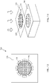
- FIG. 8 is a diagram illustrating the sensing layer 528 in FIG. 6 according to a first embodiment of the present invention.
- the sensing layer 528 in FIG 8 comprises a transparent conductive film 530, and the transparent conductive film 530 has a plurality of transparent conductive wires 532 connected to the metal pads 518.
- FIG. 9 is a diagram illustrating the sensing layer 528 in FIG. 6 according to a second embodiment of the present invention.
- the sensing layer 528 in FIG. 9 comprises two transparent conductive films 534 and 538, and the two transparent conductive films 534 and 538 are separated by an insulating layer 536.
- the insulating layer 536 may be an optical adhesive.
- the transparent conductive film 534 has a plurality of transparent conductive wires 540 connected to a portion of the metal pads 518.
- the transparent conductive film 538 has a plurality of transparent conductive wires 542 connected to the remaining of the metal pads 518.
- the material of the transparent conductive wires 532, 538 and 540 may be poly3,4-ethylenedioxythiophene or cubic boron nitride.
- the connector 516 is a zebra connector that comprises a plurality of conductive silicone strips 522 and a plurality of insulating silicone strips 524. As shown in FIG. 11 , the conductive silicone strips 522 and the insulating silicone strips 524 are arranged in an interleaved manner. Since the connector 516 in FIG. 11 is composed of conductive silicone strips 522 and insulating silicone strips 524, it may also be referred to as a silicone connector. In the embodiments of FIG. 6 and FIG. 7 , the connector 516 is L-shaped, but the invention is not limited thereto. The connector 516 may also be in other regular or irregular shapes.
- FIG. 12 is a diagram illustrating another embodiment of a retaining frame.
- the retaining frame 514 has a slot 515, and the display 512 is embedded in the slot 515.
- the metal pads 518 and the sensing layer 528 are formed on the substrate 526 to construct the touch sensor 504 as shown in FIG. 13 , and the sensing layer 528 is connected to the metal pads 518.
- the touch sensor 504 is placed in a mold 544 for thermoforming, as shown in FIG. 14 .
- the touch sensor 504 is formed into a three-dimensional touch sensor after thermoforming, and the metal pads 518 are on the inner side of the three-dimensional touch sensor 504.
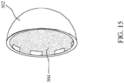
- a three-dimensional housing 502 is formed on the outside of the three-dimensional touch sensor 504 by injection molding, as shown in FIG. 15 .
- the housing 502 can be appropriately trimmed by the shaping step to obtain the desired shape, such as a housing with a spherical surface, a housing with a non-spherical surface, a regularly shaped housing, or an irregularly shaped housing.
- the lower cover 506, the circuit board 508, the display 512, the retaining frame 514 and the connector 516 shown in FIG. 7 are assembled with the housing 502 and the touch sensor 504 to obtain the touch device 500, as shown in FIG. 6 .
- the retaining frame 514 may be used to fix the connector 516 to the inner side of the touch sensor 504, and the connector 516 may be connected to the metal pads 518. Then, the metal pads 510 on the circuit board 508 are connected to the connector 516, so that the metal pads 510 are electrically connected to the metal pads 518 respectively. Finally, the lower cover 506 is combined with the housing 502 to complete the touch device 500.
Landscapes
- Engineering & Computer Science (AREA)
- General Engineering & Computer Science (AREA)
- Theoretical Computer Science (AREA)
- General Physics & Mathematics (AREA)
- Human Computer Interaction (AREA)
- Physics & Mathematics (AREA)
- Mechanical Engineering (AREA)
- Computer Networks & Wireless Communication (AREA)
- Manufacturing & Machinery (AREA)
- Position Input By Displaying (AREA)
- Devices For Indicating Variable Information By Combining Individual Elements (AREA)
- Manufacture Of Switches (AREA)
- Control Of Vending Devices And Auxiliary Devices For Vending Devices (AREA)
Applications Claiming Priority (1)
| Application Number | Priority Date | Filing Date | Title |
|---|---|---|---|
| CN202110141839.7A CN112799539B (zh) | 2021-02-02 | 2021-02-02 | 触控装置及其制作方法 |
Publications (1)
| Publication Number | Publication Date |
|---|---|
| EP4036698A1 true EP4036698A1 (fr) | 2022-08-03 |
Family
ID=74947064
Family Applications (1)
| Application Number | Title | Priority Date | Filing Date |
|---|---|---|---|
| EP21163011.6A Withdrawn EP4036698A1 (fr) | 2021-02-02 | 2021-03-16 | Dispositif de commande tactile et son procédé de fabrication |
Country Status (5)
| Country | Link |
|---|---|
| US (1) | US11334186B1 (fr) |
| EP (1) | EP4036698A1 (fr) |
| JP (1) | JP7145262B2 (fr) |
| CN (1) | CN112799539B (fr) |
| TW (1) | TWI788776B (fr) |
Families Citing this family (2)
| Publication number | Priority date | Publication date | Assignee | Title |
|---|---|---|---|---|
| TWI808413B (zh) * | 2021-04-29 | 2023-07-11 | 位元奈米科技股份有限公司 | 可用於熱壓成型之透明導電基板結構 |
| TWI845249B (zh) * | 2023-04-10 | 2024-06-11 | 達運精密工業股份有限公司 | 立體觸控裝置及其製作方法 |
Citations (6)
| Publication number | Priority date | Publication date | Assignee | Title |
|---|---|---|---|---|
| US20050205407A1 (en) * | 2004-03-17 | 2005-09-22 | Hein David A | Multi-shot molded touch switch |
| EP2416338A1 (fr) * | 2009-04-03 | 2012-02-08 | Sony Corporation | Elément d'effleurement de type capacitif et son procédé de production, et dispositif de détection par effleurement de type capacitif |
| CN103324321A (zh) * | 2012-03-20 | 2013-09-25 | 云辉科技股份有限公司 | 立体化触控模块及其制造方法 |
| US20150185889A1 (en) * | 2012-06-19 | 2015-07-02 | Nissha Printing Co., Ltd. | Touch panel and method of manufacturing the touch panel |
| EP3296845A1 (fr) * | 2015-05-11 | 2018-03-21 | FUJIFILM Corporation | Procédé de fabrication d'un stratifié conducteur, stratifié conducteur, substrat doté d'une couche précurseur à couche plaquée, substrat doté d'une couche plaquée et capteur tactile |
| CN110174965A (zh) * | 2019-05-09 | 2019-08-27 | 业成科技(成都)有限公司 | 窄边框触控面板 |
Family Cites Families (22)
| Publication number | Priority date | Publication date | Assignee | Title |
|---|---|---|---|---|
| CN101727249B (zh) * | 2008-10-31 | 2012-02-01 | 宸鸿光电科技股份有限公司 | 曲面状电容式触控板的制法 |
| US20120019449A1 (en) * | 2010-07-26 | 2012-01-26 | Atmel Corporation | Touch sensing on three dimensional objects |
| JP5916516B2 (ja) * | 2012-05-29 | 2016-05-11 | 日本写真印刷株式会社 | 3次元曲面タッチパネル及びこれを用いた電子機器筐体 |
| KR102282105B1 (ko) * | 2012-09-03 | 2021-07-26 | 가부시키가이샤 한도오따이 에네루기 켄큐쇼 | 표시 장치 및 전자 기기 |
| JP2014096061A (ja) * | 2012-11-09 | 2014-05-22 | Nissha Printing Co Ltd | タッチパネル、タッチパネルの製造方法 |
| KR20140080239A (ko) * | 2012-12-20 | 2014-06-30 | 삼성전기주식회사 | 터치 패널의 연결 구조체 및 그의 제조 방법 |
| CN103218080A (zh) * | 2013-04-12 | 2013-07-24 | 上海鼎为软件技术有限公司 | 一种触控模组及其制造方法 |
| JP2015032106A (ja) * | 2013-08-01 | 2015-02-16 | 日本写真印刷株式会社 | タッチパネル、タッチパネルの製造方法 |
| WO2015025680A1 (fr) * | 2013-08-23 | 2015-02-26 | アルプス電気株式会社 | Dispositif d'entrée de type capacité |
| TWM474931U (zh) * | 2013-12-11 | 2014-03-21 | Hannstouch Solution Inc | 觸控面板 |
| KR20170006153A (ko) * | 2015-07-07 | 2017-01-17 | 엘지이노텍 주식회사 | 터치 윈도우 |
| CN205038618U (zh) * | 2015-08-27 | 2016-02-17 | 深圳迈瑞生物医疗电子股份有限公司 | 触控显示装置 |
| CN106484164B (zh) * | 2015-08-31 | 2023-10-13 | 宸鸿科技(厦门)有限公司 | 触控面板 |
| KR101796011B1 (ko) * | 2015-11-30 | 2017-11-09 | 주식회사 트레이스 | 반구형 터치센서 판넬의 열성형 장치 |
| JP6976310B2 (ja) * | 2017-02-22 | 2021-12-08 | 富士フイルム株式会社 | 導電性フィルム、3次元形状を有する導電性フィルムおよびその製造方法、延伸フィルムの製造方法、タッチセンサーフィルム |
| CN108241452B (zh) * | 2018-01-03 | 2021-01-26 | 京东方科技集团股份有限公司 | 一种立体触摸基板及其制备方法、立体触摸显示面板 |
| CN108182013B (zh) * | 2018-02-05 | 2021-01-01 | 友达光电(苏州)有限公司 | 触控面板 |
| US11163413B2 (en) * | 2018-05-17 | 2021-11-02 | Cirque Corporation | Capacitive sensor for a three dimensional object |
| TW202016612A (zh) * | 2018-10-15 | 2020-05-01 | 大陸商深圳柔顯系統技術有限公司 | 觸控結構及觸控裝置 |
| CN109388289B (zh) * | 2018-10-31 | 2022-04-15 | 业成科技(成都)有限公司 | 触控面板以及触控面板的制造方法 |
| KR102879915B1 (ko) * | 2019-02-07 | 2025-11-04 | 삼성디스플레이 주식회사 | 전자 패널 및 이를 포함하는 전자 장치 |
| CN111104005B (zh) * | 2019-12-25 | 2023-11-14 | 业成光电(无锡)有限公司 | 触控感测模组、触控显示面板及智能手表 |
-
2021
- 2021-02-02 CN CN202110141839.7A patent/CN112799539B/zh active Active
- 2021-02-05 TW TW110104553A patent/TWI788776B/zh active
- 2021-03-12 US US17/199,767 patent/US11334186B1/en active Active
- 2021-03-12 JP JP2021040158A patent/JP7145262B2/ja active Active
- 2021-03-16 EP EP21163011.6A patent/EP4036698A1/fr not_active Withdrawn
Patent Citations (6)
| Publication number | Priority date | Publication date | Assignee | Title |
|---|---|---|---|---|
| US20050205407A1 (en) * | 2004-03-17 | 2005-09-22 | Hein David A | Multi-shot molded touch switch |
| EP2416338A1 (fr) * | 2009-04-03 | 2012-02-08 | Sony Corporation | Elément d'effleurement de type capacitif et son procédé de production, et dispositif de détection par effleurement de type capacitif |
| CN103324321A (zh) * | 2012-03-20 | 2013-09-25 | 云辉科技股份有限公司 | 立体化触控模块及其制造方法 |
| US20150185889A1 (en) * | 2012-06-19 | 2015-07-02 | Nissha Printing Co., Ltd. | Touch panel and method of manufacturing the touch panel |
| EP3296845A1 (fr) * | 2015-05-11 | 2018-03-21 | FUJIFILM Corporation | Procédé de fabrication d'un stratifié conducteur, stratifié conducteur, substrat doté d'une couche précurseur à couche plaquée, substrat doté d'une couche plaquée et capteur tactile |
| CN110174965A (zh) * | 2019-05-09 | 2019-08-27 | 业成科技(成都)有限公司 | 窄边框触控面板 |
Also Published As
| Publication number | Publication date |
|---|---|
| JP7145262B2 (ja) | 2022-09-30 |
| JP2022118676A (ja) | 2022-08-15 |
| US11334186B1 (en) | 2022-05-17 |
| CN112799539B (zh) | 2022-08-09 |
| CN112799539A (zh) | 2021-05-14 |
| TWI788776B (zh) | 2023-01-01 |
| TW202232294A (zh) | 2022-08-16 |
Similar Documents
| Publication | Publication Date | Title |
|---|---|---|
| US8471345B2 (en) | Biometric sensor assembly with integrated visual indicator | |
| TWI652517B (zh) | 用於製造電子產品的方法、相關的配置以及產品 | |
| CN107038434B (zh) | 显示装置和移动终端 | |
| CN104850289B (zh) | 无线控制系统、触控感应电极整合模块、触控感应模块及其制造方法 | |
| US10061962B2 (en) | Fingerprint identification module and manufacturing method thereof | |
| CN109076710A (zh) | 具有嵌入式多层电子器件的多层结构 | |
| CN102832068A (zh) | 一种按键装置及其导光膜层 | |
| US11334186B1 (en) | Touch control device and manufacturing method thereof | |
| US9679188B2 (en) | Fingerprint sensor packaging module and manufacturing method thereof | |
| US20170243045A1 (en) | Fingerprint identification module and manufacturing method thereof | |
| US11530808B1 (en) | Integrated multilayer structure containing optically functional module and related method of manufacture | |
| JP3172234U (ja) | 導光構造、導光構造を含むキーパッド、及びその製造方法 | |
| CN118923218A (zh) | 电子组件的制造方法及电子组件 | |
| CN106206915A (zh) | 一种光学芯片的集成结构及其制造方法 | |
| CN101447354B (zh) | 模内成型触控模组的生产方法 | |
| CN104850839A (zh) | 光学采集模组的光控制组件及成型方法 | |
| JP7269985B2 (ja) | 発光モジュール、発光モジュールの製造方法及び電子装置 | |
| CN106484164B (zh) | 触控面板 | |
| JP2020080295A (ja) | 隔壁を具えた光電機構の製作方法 | |
| CN224135833U (zh) | 一种装饰件及电子设备 | |
| JP5221784B2 (ja) | 電子機器用外観ケース | |
| TW201409512A (zh) | 一種按鍵裝置及其導光膜層 | |
| US11903147B2 (en) | Electronic device including housing and method of producing the housing | |
| KR102343006B1 (ko) | 인몰드 전자기기 타입의 인디케이터의 제조방법 | |
| WO2018066533A1 (fr) | Procédé de fabrication d'un dispositif d'entrée |
Legal Events
| Date | Code | Title | Description |
|---|---|---|---|
| PUAI | Public reference made under article 153(3) epc to a published international application that has entered the european phase |
Free format text: ORIGINAL CODE: 0009012 |
|
| STAA | Information on the status of an ep patent application or granted ep patent |
Free format text: STATUS: THE APPLICATION HAS BEEN PUBLISHED |
|
| AK | Designated contracting states |
Kind code of ref document: A1 Designated state(s): AL AT BE BG CH CY CZ DE DK EE ES FI FR GB GR HR HU IE IS IT LI LT LU LV MC MK MT NL NO PL PT RO RS SE SI SK SM TR |
|
| STAA | Information on the status of an ep patent application or granted ep patent |
Free format text: STATUS: REQUEST FOR EXAMINATION WAS MADE |
|
| 17P | Request for examination filed |
Effective date: 20220826 |
|
| RBV | Designated contracting states (corrected) |
Designated state(s): AL AT BE BG CH CY CZ DE DK EE ES FI FR GB GR HR HU IE IS IT LI LT LU LV MC MK MT NL NO PL PT RO RS SE SI SK SM TR |
|
| STAA | Information on the status of an ep patent application or granted ep patent |
Free format text: STATUS: EXAMINATION IS IN PROGRESS |
|
| 17Q | First examination report despatched |
Effective date: 20231122 |
|
| RAP1 | Party data changed (applicant data changed or rights of an application transferred) |
Owner name: GENERAL INTERFACE SOLUTION LIMITED Owner name: INTERFACE OPTOELECTRONICS (SHENZHEN) CO., LTD. Owner name: INTERFACE TECHNOLOGY (CHENGDU) CO., LTD. |
|
| GRAP | Despatch of communication of intention to grant a patent |
Free format text: ORIGINAL CODE: EPIDOSNIGR1 |
|
| STAA | Information on the status of an ep patent application or granted ep patent |
Free format text: STATUS: GRANT OF PATENT IS INTENDED |
|
| INTG | Intention to grant announced |
Effective date: 20250305 |
|
| STAA | Information on the status of an ep patent application or granted ep patent |
Free format text: STATUS: THE APPLICATION IS DEEMED TO BE WITHDRAWN |
|
| 18D | Application deemed to be withdrawn |
Effective date: 20250708 |