EP4037172A1 - Circuit de convertisseur de puissance résonant - Google Patents
Circuit de convertisseur de puissance résonant Download PDFInfo
- Publication number
- EP4037172A1 EP4037172A1 EP22153288.0A EP22153288A EP4037172A1 EP 4037172 A1 EP4037172 A1 EP 4037172A1 EP 22153288 A EP22153288 A EP 22153288A EP 4037172 A1 EP4037172 A1 EP 4037172A1
- Authority
- EP
- European Patent Office
- Prior art keywords
- transformer
- circuit
- output voltage
- winding
- controller
- Prior art date
- Legal status (The legal status is an assumption and is not a legal conclusion. Google has not performed a legal analysis and makes no representation as to the accuracy of the status listed.)
- Pending
Links
Images


Classifications
-
- H—ELECTRICITY
- H02—GENERATION; CONVERSION OR DISTRIBUTION OF ELECTRIC POWER
- H02M—APPARATUS FOR CONVERSION BETWEEN AC AND AC, BETWEEN AC AND DC, OR BETWEEN DC AND DC, AND FOR USE WITH MAINS OR SIMILAR POWER SUPPLY SYSTEMS; CONVERSION OF DC OR AC INPUT POWER INTO SURGE OUTPUT POWER; CONTROL OR REGULATION THEREOF
- H02M3/00—Conversion of DC power input into DC power output
- H02M3/01—Resonant DC/DC converters
-
- H—ELECTRICITY
- H02—GENERATION; CONVERSION OR DISTRIBUTION OF ELECTRIC POWER
- H02M—APPARATUS FOR CONVERSION BETWEEN AC AND AC, BETWEEN AC AND DC, OR BETWEEN DC AND DC, AND FOR USE WITH MAINS OR SIMILAR POWER SUPPLY SYSTEMS; CONVERSION OF DC OR AC INPUT POWER INTO SURGE OUTPUT POWER; CONTROL OR REGULATION THEREOF
- H02M3/00—Conversion of DC power input into DC power output
- H02M3/22—Conversion of DC power input into DC power output with intermediate conversion into AC
- H02M3/24—Conversion of DC power input into DC power output with intermediate conversion into AC by static converters
- H02M3/28—Conversion of DC power input into DC power output with intermediate conversion into AC by static converters using discharge tubes with control electrode or semiconductor devices with control electrode to produce the intermediate AC
- H02M3/325—Conversion of DC power input into DC power output with intermediate conversion into AC by static converters using discharge tubes with control electrode or semiconductor devices with control electrode to produce the intermediate AC using devices of a triode or a transistor type requiring continuous application of a control signal
- H02M3/335—Conversion of DC power input into DC power output with intermediate conversion into AC by static converters using discharge tubes with control electrode or semiconductor devices with control electrode to produce the intermediate AC using devices of a triode or a transistor type requiring continuous application of a control signal using semiconductor devices only
- H02M3/33569—Conversion of DC power input into DC power output with intermediate conversion into AC by static converters using discharge tubes with control electrode or semiconductor devices with control electrode to produce the intermediate AC using devices of a triode or a transistor type requiring continuous application of a control signal using semiconductor devices only having several active switching elements
-
- H—ELECTRICITY
- H02—GENERATION; CONVERSION OR DISTRIBUTION OF ELECTRIC POWER
- H02M—APPARATUS FOR CONVERSION BETWEEN AC AND AC, BETWEEN AC AND DC, OR BETWEEN DC AND DC, AND FOR USE WITH MAINS OR SIMILAR POWER SUPPLY SYSTEMS; CONVERSION OF DC OR AC INPUT POWER INTO SURGE OUTPUT POWER; CONTROL OR REGULATION THEREOF
- H02M1/00—Details of apparatus for conversion
- H02M1/0003—Details of control, feedback or regulation circuits
-
- H—ELECTRICITY
- H02—GENERATION; CONVERSION OR DISTRIBUTION OF ELECTRIC POWER
- H02M—APPARATUS FOR CONVERSION BETWEEN AC AND AC, BETWEEN AC AND DC, OR BETWEEN DC AND DC, AND FOR USE WITH MAINS OR SIMILAR POWER SUPPLY SYSTEMS; CONVERSION OF DC OR AC INPUT POWER INTO SURGE OUTPUT POWER; CONTROL OR REGULATION THEREOF
- H02M1/00—Details of apparatus for conversion
- H02M1/08—Circuits specially adapted for the generation of control voltages for semiconductor devices incorporated in static converters
- H02M1/088—Circuits specially adapted for the generation of control voltages for semiconductor devices incorporated in static converters for the simultaneous control of series or parallel connected semiconductor devices
- H02M1/092—Circuits specially adapted for the generation of control voltages for semiconductor devices incorporated in static converters for the simultaneous control of series or parallel connected semiconductor devices the control signals being transmitted optically
-
- H—ELECTRICITY
- H02—GENERATION; CONVERSION OR DISTRIBUTION OF ELECTRIC POWER
- H02M—APPARATUS FOR CONVERSION BETWEEN AC AND AC, BETWEEN AC AND DC, OR BETWEEN DC AND DC, AND FOR USE WITH MAINS OR SIMILAR POWER SUPPLY SYSTEMS; CONVERSION OF DC OR AC INPUT POWER INTO SURGE OUTPUT POWER; CONTROL OR REGULATION THEREOF
- H02M3/00—Conversion of DC power input into DC power output
- H02M3/22—Conversion of DC power input into DC power output with intermediate conversion into AC
- H02M3/24—Conversion of DC power input into DC power output with intermediate conversion into AC by static converters
- H02M3/28—Conversion of DC power input into DC power output with intermediate conversion into AC by static converters using discharge tubes with control electrode or semiconductor devices with control electrode to produce the intermediate AC
- H02M3/325—Conversion of DC power input into DC power output with intermediate conversion into AC by static converters using discharge tubes with control electrode or semiconductor devices with control electrode to produce the intermediate AC using devices of a triode or a transistor type requiring continuous application of a control signal
- H02M3/335—Conversion of DC power input into DC power output with intermediate conversion into AC by static converters using discharge tubes with control electrode or semiconductor devices with control electrode to produce the intermediate AC using devices of a triode or a transistor type requiring continuous application of a control signal using semiconductor devices only
- H02M3/33507—Conversion of DC power input into DC power output with intermediate conversion into AC by static converters using discharge tubes with control electrode or semiconductor devices with control electrode to produce the intermediate AC using devices of a triode or a transistor type requiring continuous application of a control signal using semiconductor devices only with automatic control of the output voltage or current, e.g. flyback converters
-
- H—ELECTRICITY
- H03—ELECTRONIC CIRCUITRY
- H03K—PULSE TECHNIQUE
- H03K17/00—Electronic switching or gating, i.e. not by contact-making and –breaking
- H03K17/51—Electronic switching or gating, i.e. not by contact-making and –breaking characterised by the components used
- H03K17/56—Electronic switching or gating, i.e. not by contact-making and –breaking characterised by the components used by the use, as active elements, of semiconductor devices
- H03K17/687—Electronic switching or gating, i.e. not by contact-making and –breaking characterised by the components used by the use, as active elements, of semiconductor devices the devices being field-effect transistors
- H03K17/689—Electronic switching or gating, i.e. not by contact-making and –breaking characterised by the components used by the use, as active elements, of semiconductor devices the devices being field-effect transistors with galvanic isolation between the control circuit and the output circuit
- H03K17/691—Electronic switching or gating, i.e. not by contact-making and –breaking characterised by the components used by the use, as active elements, of semiconductor devices the devices being field-effect transistors with galvanic isolation between the control circuit and the output circuit using transformer coupling
-
- H—ELECTRICITY
- H03—ELECTRONIC CIRCUITRY
- H03K—PULSE TECHNIQUE
- H03K2217/00—Indexing scheme related to electronic switching or gating, i.e. not by contact-making or -breaking covered by H03K17/00
- H03K2217/0081—Power supply means, e.g. to the switch driver
-
- Y—GENERAL TAGGING OF NEW TECHNOLOGICAL DEVELOPMENTS; GENERAL TAGGING OF CROSS-SECTIONAL TECHNOLOGIES SPANNING OVER SEVERAL SECTIONS OF THE IPC; TECHNICAL SUBJECTS COVERED BY FORMER USPC CROSS-REFERENCE ART COLLECTIONS [XRACs] AND DIGESTS
- Y02—TECHNOLOGIES OR APPLICATIONS FOR MITIGATION OR ADAPTATION AGAINST CLIMATE CHANGE
- Y02B—CLIMATE CHANGE MITIGATION TECHNOLOGIES RELATED TO BUILDINGS, e.g. HOUSING, HOUSE APPLIANCES OR RELATED END-USER APPLICATIONS
- Y02B70/00—Technologies for an efficient end-user side electric power management and consumption
- Y02B70/10—Technologies improving the efficiency by using switched-mode power supplies [SMPS], i.e. efficient power electronics conversion e.g. power factor correction or reduction of losses in power supplies or efficient standby modes
Definitions
- the present specification relates to systems, methods, apparatuses, devices, articles of manufacture and instructions for power supplies.
- a switch mode power supply (SMPS) circuit configured to receive an input voltage and generate an output voltage, comprising: a set of switching devices configured to receive the input voltage; a first transformer, having an input winding coupled to the switching devices, and an output winding configured to generate the output voltage; a second transformer, having an input winding coupled to receive the output voltage from the first transformer, and an output winding configured to generate an output voltage monitoring signal; and a controller configured to control the switching devices based on the output voltage monitoring signal.
- SMPS switch mode power supply
- the controller is configured to control the switching devices based only on the output voltage monitoring signal.
- the output voltage monitoring signal is also configured as a power supply for the switch mode power supply.
- the output voltage monitoring signal is also configured as a power supply for the controller.
- the controller is solely powered by the output voltage monitoring signal.
- the controller is solely powered by the output voltage monitoring signal after the switch mode power supply circuit reaches a stable operating state.
- the input voltage is a rectified supply (Vbus) voltage.
- the switching devices form a half-bridge.
- the input winding of the second transformer is coupled directly to the output winding of the first transformer.
- the output winding of the second transformer is coupled directly to the controller.
- the first transformer is a resonant transformer and the second transformer is an auxiliary transformer.
- the switch mode power supply is a resonant power converter.
- a ratio of a number of wire turns in the input winding to a number of wire turns in the output winding is a non-integer number.
- the output winding of the second transformer is center tapped to enable full wave rectification.
- a magnetic flux of the first transformer is isolated from a magnetic flux of the second transformer.
- the output winding of the first transformer is configured to be coupled to a load drawing a load current; and the second transformer is configured to draw a current that is independent of the load current.
- the switching devices are switching transistors.
- the controller is also configured to receive the input voltage as a power supply for the controller.
- a resonant power converter configured to receive an input voltage and generate an output voltage, comprising: a set of switching devices configured to receive the input voltage; a first transformer, having an input winding coupled to the switching devices, and an output winding configured to generate the output voltage; a second transformer, having an input winding coupled to receive the output voltage, and an output winding configured to generate an output voltage monitoring signal; and a controller configured to control switching of the switching devices based on the output voltage monitoring signal.
- Switch mode power supplies are used in many power supply applications for many electronic devices. At start-up, such Switch mode power supplies may be bootstrapped by a rectified supply voltage, but then quickly switch to being powered by their own regulated output voltages sent to a set of downstream circuits to be supplied and protected.
- Such switch mode power supplies are also configured to receive a sensing and/or monitoring signal that is intended to roughly parallel the switch mode power supplies' actual output voltage and which is used for supply of the controller and/or feedback for protection and/or regulation of the output voltage.
- some switch mode power supplies use an auxiliary winding from a same transformer to generate the sensing signal.
- FIG. 1 represents an example 100 switch mode power supply 102 with a single transformer.
- the example 100 includes the switch mode power supply 102 coupled to receive an input voltage (Vbus) 104 and generate an output voltage (Vout) 106.
- the switch mode power supply 102 includes a controller 108, switching devices 110, an LC circuit (formed by Ls, Lm, Cr as shown in Figure 1 ) and a transformer 114.
- the transformer 114 includes input winding 116 on a primary/high-voltage/hot side, output winding 118 on a secondary/low-voltage/cold side, and an auxiliary winding 120.
- the controller 108 can be split up into a controller and a level shifter.
- the controller 108 chip is placed on the primary/high-voltage/hot side and connected to the input winding 116 and to the auxiliary winding 120.
- the controller 108 controls the switching devices 110 (e.g. switching transistors) that are coupled by the LC circuit to the transformer 114 to control the output voltage (Vout) 106.
- An optical control circuit 122 provides output voltage (Vout) 106 feedback to the controller 108 for controlling the switching devices 110.
- the controller 108 can also use the auxiliary winding 120 to indirectly sense/monitor the output voltage (Vout) 106.
- the controller 108 chip is directly supplied from the input voltage (Vbus) 104 (i.e. high-voltage rectified voltage (Vbus)).
- Vbus input voltage
- the controller 108 chip may be also supplied from auxiliary winding 120 on the transformer 114 as shown in Figure 1 .
- the secondary output winding 118 and the auxiliary winding 120 are center tapped to enable full wave rectification.
- a secondary winding output voltage from the output winding 118 is provided to a rectification circuit, represented by diodes D1, D2 but which in some applications (e.g. high power) can be any variety of synchronous rectification circuits.
- Figure 2 represents an example 200 of the single transformer 114 in the switch mode power supply 102.
- the example 200 transformer 114 shows: the input winding 116 (e.g. primary winding) having Nprim turns and Rprim 202 total winding resistance; the output winding 118 (e.g. secondary winding) having Nsec turns and Rsec 204/206 total winding resistance on either side of the center-tap; and the auxiliary winding 120 having Naux turns and Raux 208 total winding resistance.
- a secondary winding output voltage (Vsec) 202 is shown as generated by the output winding 118.
- the auxiliary voltage (V aux ) is in the first order determined by the turns ratio N aux /N sec and the secondary winding output voltage (Vsec) 202.
- the V aux is not only used to supply the controller 108 chip (IC), but also for output overvoltage/undervoltage detection because the V aux ideally should reflect the value of the secondary winding output voltage (Vsec) 202.
- Vout is kept constant by using either the optical control circuit 122 coupled to the controller 108 (e.g. labeled SNSFB in Figure 1 ) or by feeding Vaux into the controller 108 chip (e.g. labeled SNSOUT in Figure 1 ) which then controls the switching devices 110 so that the secondary voltage (Vsec) will also be constant and at a selected regulated voltage value.
- an end result of this circuit configuration is an auxiliary voltage (V aux ) that rises when the output current increases, and thus the auxiliary voltage would not reliably mimic the output voltage (Vout) 106 anymore and could not be used for output voltage (Vout) 106 overvoltage detection.
- V aux auxiliary voltage
- the V aux rise at high secondary output currents can become so large that V aux exceeds a maximum supply voltage of the controller 108 chip and thus could damage the controller 108.
- the output/secondary winding 118 consists of only one winding. Because then the turns ratio N aux /N sec is a whole number, the auxiliary voltage is a multiple of the output voltage (Vout) 106. For example, if the output voltage (Vout) 106 is 12V, then the auxiliary voltage would be 12V, 24V, 36V, and so on depending upon the number of whole turns. Since the controller 108 chip could have a limited supply voltage (e.g. labeled SUPIC (Supply IC) in Figure 1 ) range, together with an auxiliary voltage rise at higher currents, the controller 108 could not use the auxiliary winding as a power supply for the controller 108 chip.
- SUPIC SUPIC
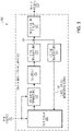
- Figure 3 represents a first example 300 switch mode power supply 302 with two transformers.
- the example 300 switch mode power supply 302 is coupled to receive an input voltage 304 and generate an output voltage 306.
- the switch mode power supply 302 includes a controller 308, switching devices 310 (e.g. transistors), an LC circuit 312, a first transformer 314, a second transformer 316, and a rectification circuit 320.
- the controller 308 in some example embodiments is coupled to receive the input voltage 304.
- the set of switching devices 310 e.g. switching transistors
- the first transformer 314 includes an input/primary winding coupled to the switching devices 310 via the LC circuit 312.
- the first transformer 314 also includes an output/secondary winding configured to generate a secondary winding output voltage 322.
- the rectification circuit 320 receives the secondary winding output voltage 322 and generates the output voltage 306.
- the second transformer 316 is not flux coupled to the first transformer 314, but instead has its own input/primary winding coupled to directly receive the secondary winding output voltage 322.
- the second transformer 316 also includes an output/secondary winding configured to generate an output voltage monitoring signal 318 from the secondary winding output voltage 322.
- the controller 308 is configured to control the switching devices 310 and thus the output voltage 306, based on the output voltage monitoring signal 318.
- the output voltage monitoring signal 318 is also used as a power supply for the switch mode power supply 302 and/or the controller 308.
- the example 300 switch mode power supply 302 thus provides an option of providing an output voltage 306 without a need for an additional controller or switches, either on the primary or secondary side of the first transformer 314.
- the switch mode power supply 302 is a resonant power converter.
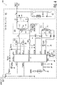
- Figure 4 represents a second example 400 switch mode power supply 402 with two transformers.
- the example 400 switch mode power supply 402 is configured to receive an input voltage (Vbus) 404 and generate an output voltage (Vout) 406.
- the switch mode power supply 402 includes a controller 408, switching devices 410, an LC circuit (formed by Ls, Lm, Cr as shown in Figure 4 ), a first transformer 414, a second transformer 420, and an optical control circuit 428.
- the first transformer 414 includes input winding 416 and output winding 418.
- the second transformer 420 includes an input winding 422, an output winding 424 and is configured to generate an output voltage monitoring/sensing signal 426 from a secondary winding output voltage (Vsec) 430.
- the optical control circuit 428 provides output voltage (Vout) 406 feedback to the controller 408 for controlling the switching devices 410.
- the controller 408 can also use the second transformer 420 to directly sense/monitor the secondary winding output voltage 430 for better regulation of the output voltage (Vout) 406.
- the switch mode power supply 402 operates in a manner similar to that discussed for the switch mode power supply 302 in Figure 3 .
- the first transformer 414 and the second transformer 420 are not flux coupled.
- the concern that high output currents from the first transformer 414 would affect the output voltage monitoring/sensing signal 426 based on the output voltage (Vout) 406 is no longer a concern.
- the separate second transformer 420 to generate the output voltage monitoring/sensing signal 426, instead of using a voltage from an auxiliary winding coupled to the first transformer 414 (as discussed in Figures 1 and 2 ) has the advantage that the output voltage monitoring/sensing signal 426 is not distorted by the secondary current from the first transformer 414 since the output voltage monitoring/sensing signal 426 is now based on the secondary voltage (Vsec) rather than the shared flux from the primary winding 416 in the transformer 414. In this way the output voltage monitoring/sensing signal 426 voltage is a reliable reflection of the output voltage (Vout) 406.
- Vout 406 is to be regulated to 12V and the controller's 408 supply voltage (SUPIC) is to be 18V.
- SUPIC supply voltage
- a diode i.e. the diode between the second transformer 420 and the controller 408 forward voltage is 0.6V.
- Vsec 12.6V
- these instructions/steps are implemented as functional and software instructions.
- the instructions can be implemented either using logic gates, application specific chips, firmware, as well as other hardware forms.
Landscapes
- Engineering & Computer Science (AREA)
- Power Engineering (AREA)
- Dc-Dc Converters (AREA)
Applications Claiming Priority (1)
| Application Number | Priority Date | Filing Date | Title |
|---|---|---|---|
| US17/161,094 US11817787B2 (en) | 2021-01-28 | 2021-01-28 | Switch mode power supply (SMPS) circuit |
Publications (1)
| Publication Number | Publication Date |
|---|---|
| EP4037172A1 true EP4037172A1 (fr) | 2022-08-03 |
Family
ID=80034861
Family Applications (1)
| Application Number | Title | Priority Date | Filing Date |
|---|---|---|---|
| EP22153288.0A Pending EP4037172A1 (fr) | 2021-01-28 | 2022-01-25 | Circuit de convertisseur de puissance résonant |
Country Status (3)
| Country | Link |
|---|---|
| US (1) | US11817787B2 (fr) |
| EP (1) | EP4037172A1 (fr) |
| CN (1) | CN114825949A (fr) |
Citations (7)
| Publication number | Priority date | Publication date | Assignee | Title |
|---|---|---|---|---|
| US4106084A (en) * | 1975-01-10 | 1978-08-08 | Societe Nationale Des Petroles D'aquitaine | Means for controlling the electric current density of a high tension direct current source |
| US5757627A (en) * | 1996-05-01 | 1998-05-26 | Compaq Computer Corporation | Isolated power conversion with master controller in secondary |
| US20080101103A1 (en) * | 2006-10-25 | 2008-05-01 | Sanken Electric Co., Ltd. | Power conversion apparatus and method of controlling the same |
| WO2013111290A1 (fr) * | 2012-01-25 | 2013-08-01 | イサハヤ電子株式会社 | Régulateur de commutation |
| EP2837262B1 (fr) * | 2012-04-13 | 2019-01-09 | Tridonic GmbH & Co. KG | Procédé permettant de faire fonctionner un transducteur à résonance llc pour un moyen d'éclairage, transducteur et convertisseur pour del |
| US10250126B1 (en) * | 2018-02-12 | 2019-04-02 | Meanwell (Guangzhou) Electronics Co., Ltd. | Method for controlling resonant converter |
| US20200280313A1 (en) * | 2017-10-06 | 2020-09-03 | Heyday Integrated Circuits Sas | Galvanically isolated low-latency switch drive circuit with power transfer |
Family Cites Families (14)
| Publication number | Priority date | Publication date | Assignee | Title |
|---|---|---|---|---|
| US4232280A (en) * | 1979-03-08 | 1980-11-04 | Hughes Aircraft Company | Network for simulating low temperature resistors |
| US4439821A (en) * | 1982-01-29 | 1984-03-27 | Varo, Inc. | DC to DC switching regulator with temperature compensated isolated feedback circuitry |
| US4495554A (en) | 1983-03-28 | 1985-01-22 | International Business Machines Corporation | Isolated power supply feedback |
| CN1050242C (zh) * | 1993-06-14 | 2000-03-08 | Vlt公司 | 电源变换装置、电源变换器控制装置及其制造电源变换器的方法 |
| US6018467A (en) * | 1999-07-28 | 2000-01-25 | Philips Electronics North America Corporation | Resonant mode power supply having an efficient low power stand-by mode |
| US6154375A (en) * | 1999-10-08 | 2000-11-28 | Philips Electronics North America Corporation | Soft start scheme for resonant converters having variable frequency control |
| JP4661304B2 (ja) * | 2005-03-28 | 2011-03-30 | パナソニック電工株式会社 | 無電極放電灯点灯装置及び照明器具 |
| US7225706B2 (en) * | 2005-06-09 | 2007-06-05 | Rotor Clip Company, Inc. | Tool for hose clamps |
| EP2176944B1 (fr) | 2007-07-04 | 2016-10-19 | Nxp B.V. | Fonctionnement en mode veille d'un convertisseur de puissance à résonance |
| EP2469696B1 (fr) | 2010-12-23 | 2018-10-24 | Nxp B.V. | Contrôleur pour convertisseur résonant |
| CN104578826B (zh) * | 2014-12-31 | 2018-10-19 | 上海新进半导体制造有限公司 | 开关电源及在开关电源中提供恒压和恒流控制的方法 |
| US10868473B2 (en) * | 2015-11-30 | 2020-12-15 | Semiconductor Components Industries, Llc | Secondary side controlled control circuit for power converter with synchronous rectifier |
| CN111342661A (zh) * | 2018-12-19 | 2020-06-26 | 台达电子工业股份有限公司 | Llc谐振变换系统 |
| US10951107B2 (en) * | 2019-06-27 | 2021-03-16 | Cypress Semiconductor Corporation | Communicating fault indications between primary and secondary controllers in a secondary-controlled flyback converter |
-
2021
- 2021-01-28 US US17/161,094 patent/US11817787B2/en active Active
-
2022
- 2022-01-25 EP EP22153288.0A patent/EP4037172A1/fr active Pending
- 2022-01-27 CN CN202210100119.0A patent/CN114825949A/zh active Pending
Patent Citations (7)
| Publication number | Priority date | Publication date | Assignee | Title |
|---|---|---|---|---|
| US4106084A (en) * | 1975-01-10 | 1978-08-08 | Societe Nationale Des Petroles D'aquitaine | Means for controlling the electric current density of a high tension direct current source |
| US5757627A (en) * | 1996-05-01 | 1998-05-26 | Compaq Computer Corporation | Isolated power conversion with master controller in secondary |
| US20080101103A1 (en) * | 2006-10-25 | 2008-05-01 | Sanken Electric Co., Ltd. | Power conversion apparatus and method of controlling the same |
| WO2013111290A1 (fr) * | 2012-01-25 | 2013-08-01 | イサハヤ電子株式会社 | Régulateur de commutation |
| EP2837262B1 (fr) * | 2012-04-13 | 2019-01-09 | Tridonic GmbH & Co. KG | Procédé permettant de faire fonctionner un transducteur à résonance llc pour un moyen d'éclairage, transducteur et convertisseur pour del |
| US20200280313A1 (en) * | 2017-10-06 | 2020-09-03 | Heyday Integrated Circuits Sas | Galvanically isolated low-latency switch drive circuit with power transfer |
| US10250126B1 (en) * | 2018-02-12 | 2019-04-02 | Meanwell (Guangzhou) Electronics Co., Ltd. | Method for controlling resonant converter |
Also Published As
| Publication number | Publication date |
|---|---|
| US20220239232A1 (en) | 2022-07-28 |
| CN114825949A (zh) | 2022-07-29 |
| US11817787B2 (en) | 2023-11-14 |
Similar Documents
| Publication | Publication Date | Title |
|---|---|---|
| US5459652A (en) | Boot strap circuit for power up control of power supplies | |
| US6807075B2 (en) | Start-up circuit for switched mode power supply | |
| CN101997435B (zh) | 具有在次级侧上的主控制器和在初级侧上的从控制器的隔离式ac-dc转换器及其操作方法 | |
| US9391525B2 (en) | Power system switch protection using output driver regulation | |
| US8149597B2 (en) | Intermediate bus architecture with a quasi-regulated bus converter | |
| US8891997B2 (en) | Power supply system for stopping and starting operation in accordance with input voltage and image forming apparatus including the same | |
| US20030067794A1 (en) | Synchronous rectifier controller | |
| EP1081838B1 (fr) | Méthode et dispositif de contrôle de puissance, et alimentation de puissance | |
| JP2013059234A (ja) | 電源装置及び画像形成装置 | |
| EP1990884B1 (fr) | Appareil d'alimentation electrique et son procede de commande | |
| KR20060012955A (ko) | 스위칭 모드 파워 서플라이와 그 스위칭 제어 장치 | |
| JP2009296790A (ja) | スイッチング電源装置 | |
| EP4037172A1 (fr) | Circuit de convertisseur de puissance résonant | |
| US7061776B2 (en) | Half-bridge flyback power converter | |
| US6693812B1 (en) | Bias supply selection circuit, method of operation thereof and power supply employing the same | |
| US11777410B2 (en) | Power supply apparatus for stabilizing power supply capability of auxiliary winding provided in transformer | |
| US20120163034A1 (en) | Switching mode power supply having multiple output | |
| WO2021021870A1 (fr) | Convertisseur doté d'un circuit de maintien et circuit de commande d'appel | |
| US12500515B2 (en) | Resonance power supply circuit | |
| US6400587B1 (en) | Universal input flyback with secondary shunt voltage limiter | |
| JP2012135116A (ja) | スイッチング電源装置 | |
| JP5575610B2 (ja) | 電源装置 | |
| US9479068B2 (en) | Power supply device | |
| CN220291729U (zh) | 电源切换电路 | |
| JP3008081B2 (ja) | 無停電性スイッチングレギュレータ |
Legal Events
| Date | Code | Title | Description |
|---|---|---|---|
| PUAI | Public reference made under article 153(3) epc to a published international application that has entered the european phase |
Free format text: ORIGINAL CODE: 0009012 |
|
| STAA | Information on the status of an ep patent application or granted ep patent |
Free format text: STATUS: THE APPLICATION HAS BEEN PUBLISHED |
|
| AK | Designated contracting states |
Kind code of ref document: A1 Designated state(s): AL AT BE BG CH CY CZ DE DK EE ES FI FR GB GR HR HU IE IS IT LI LT LU LV MC MK MT NL NO PL PT RO RS SE SI SK SM TR |
|
| STAA | Information on the status of an ep patent application or granted ep patent |
Free format text: STATUS: REQUEST FOR EXAMINATION WAS MADE |
|
| 17P | Request for examination filed |
Effective date: 20230203 |
|
| RBV | Designated contracting states (corrected) |
Designated state(s): AL AT BE BG CH CY CZ DE DK EE ES FI FR GB GR HR HU IE IS IT LI LT LU LV MC MK MT NL NO PL PT RO RS SE SI SK SM TR |
|
| STAA | Information on the status of an ep patent application or granted ep patent |
Free format text: STATUS: EXAMINATION IS IN PROGRESS |
|
| 17Q | First examination report despatched |
Effective date: 20240209 |