EP4037190A1 - Système et procédé de génération de division de fréquence verrouillée sous-harmonique et d'interpolation de phase - Google Patents
Système et procédé de génération de division de fréquence verrouillée sous-harmonique et d'interpolation de phase Download PDFInfo
- Publication number
- EP4037190A1 EP4037190A1 EP22153737.6A EP22153737A EP4037190A1 EP 4037190 A1 EP4037190 A1 EP 4037190A1 EP 22153737 A EP22153737 A EP 22153737A EP 4037190 A1 EP4037190 A1 EP 4037190A1
- Authority
- EP
- European Patent Office
- Prior art keywords
- signal
- phase
- stages
- differential delay
- input
- Prior art date
- Legal status (The legal status is an assumption and is not a legal conclusion. Google has not performed a legal analysis and makes no representation as to the accuracy of the status listed.)
- Pending
Links
Images


Classifications
-
- H—ELECTRICITY
- H03—ELECTRONIC CIRCUITRY
- H03L—AUTOMATIC CONTROL, STARTING, SYNCHRONISATION OR STABILISATION OF GENERATORS OF ELECTRONIC OSCILLATIONS OR PULSES
- H03L7/00—Automatic control of frequency or phase; Synchronisation
- H03L7/24—Automatic control of frequency or phase; Synchronisation using a reference signal directly applied to the generator
-
- H—ELECTRICITY
- H03—ELECTRONIC CIRCUITRY
- H03K—PULSE TECHNIQUE
- H03K3/00—Circuits for generating electric pulses; Monostable, bistable or multistable circuits
- H03K3/02—Generators characterised by the type of circuit or by the means used for producing pulses
- H03K3/027—Generators characterised by the type of circuit or by the means used for producing pulses by the use of logic circuits, with internal or external positive feedback
- H03K3/03—Astable circuits
- H03K3/0315—Ring oscillators
- H03K3/0322—Ring oscillators with differential cells
-
- H—ELECTRICITY
- H03—ELECTRONIC CIRCUITRY
- H03K—PULSE TECHNIQUE
- H03K5/00—Manipulating of pulses not covered by one of the other main groups of this subclass
- H03K5/01—Shaping pulses
-
- H—ELECTRICITY
- H03—ELECTRONIC CIRCUITRY
- H03K—PULSE TECHNIQUE
- H03K5/00—Manipulating of pulses not covered by one of the other main groups of this subclass
- H03K2005/00013—Delay, i.e. output pulse is delayed after input pulse and pulse length of output pulse is dependent on pulse length of input pulse
- H03K2005/00078—Fixed delay
Definitions
- the present disclosure relates generally to clock generation and more particularly to injection locked phase interpolation techniques for clock generation at a receiving device.
- Demodulation and decoding of modulated signals at a receiver may involve generating reference In-phase (I) and Quadrature-phase (Q) signals to achieve precise sampling synchronized with data symbols.
- I and Q reference signals One technique for generating such I and Q reference signals, known as a fundamental harmonic injection locked phase interpolation technique, reduces the number of required input phases as compared to mixer based schemes.
- a fundamental harmonic injection locked phase interpolation technique may suffer from a narrow frequency locking range and poor systematic IQ skew.
- a system for generating sub-harmonically injection locked phase interpolated output signal comprises ring oscillator (RO) circuitry to generate an output oscillator signal in response to a periodic input signal.
- the RO circuitry includes a plurality of differential delay RO stages interconnected in cascade within a closed loop, where each of the plurality of differential delay RO stages is configured to establish a corresponding delayed version of the output oscillator signal successively shifted in phase by a predetermined phase difference based on a predetermined interpolation mapping scheme.
- the system further comprises signal injection circuitry coupled to the RO circuitry to apply first and second input signals having a first input phase and a second input phase, respectively, to the plurality of differential delay RO stages based on the predetermined interpolation mapping scheme, to lock a frequency of the output oscillator signal at one half the frequency of the periodic input signal.
- a method for generating sub-harmonically injection locked phase interpolated output signal comprises generating an output oscillator signal in response to a periodic input signal injected to a Ring Oscillator (RO), where the RO includes a plurality of differential delay RO stages interconnected in cascade within a closed loop, wherein each of the plurality of differential delay RO stages is configured to establish a corresponding delayed form of the output oscillator signal successively shifted in phase by a predetermined phase difference based on a predetermined interpolation mapping scheme.
- RO Ring Oscillator
- the method further comprises applying a first signal having a first input phase and a second signal having a second input phase to the plurality of differential delay RO stages based on the predetermined interpolation mapping scheme to lock a frequency of the output oscillator signal at one half the frequency of the periodic input signal.
- a phrase such as "apply a first phase" to another component is intended to mean “apply a signal having a first phase” to that component.
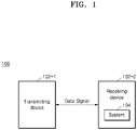
- FIG. 1 illustrates a network system 100 implementing a system 104 for a sub-harmonically locked divide-by-2 phase interpolation, according to an embodiment of the present subject matter.
- Network system 100 may include a transmitting device 102-1 that transmits data signals to a receiving device 102-2.
- the system 104 may be implemented in receiving device 102-2.
- devices 102 are user devices such as a laptop, a desktop, a smartphone, a tablet, and a desktop computer. If data is also transmitted from device 102-2 to device 102-1, a similar or identical system 104 may be incorporated within device 102-1.
- the transmitting device 102-1 and receiving device 102-2 include a base station, a portable computing device, a television, or any other computing device.
- the transmitting device 102-1 and the receiving device 102-2 may be connected to each other via a high speed interface, such as but not limited to M-PHY, High-Definition Multimedia Interface (HDMI), DisplayPort (DP) and Embedded DisplayPort (eDP), Peripheral Component Interconnect Express (PCIe), and, Universal Serial Bus (USB).
- a high speed interface such as but not limited to M-PHY, High-Definition Multimedia Interface (HDMI), DisplayPort (DP) and Embedded DisplayPort (eDP), Peripheral Component Interconnect Express (PCIe), and, Universal Serial Bus (USB).
- HDMI High-Definition Multimedia Interface
- DP DisplayPort
- eDP Embedded DisplayPort
- PCIe Peripheral Component Interconnect Express
- USB Universal Serial Bus
- the receiving device 102-2 receives the data signal from the transmitting device 102-1, where the data signal may be a digital signal or an analog signal.
- the system 104 may be configured to receive the data, detect a phase shift in data, and shift a phase of an input periodic signal, e.g., a reference signal. In this manner, the reference signal may be synchronized with the data signal, whereby sampling may occur at a central time point within a data symbol interval of the data signal.
- the system 104 may perform frequency division and interpolation based on a predetermined mapping scheme, such that an obtained output frequency is one half of an injected signal frequency. Examples of components and operations of system 104 are described hereafter in connection with FIGS. 2-4 .
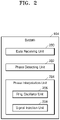
- FIG. 2 illustrates a schematic block diagram of the system 104, according to an embodiment of the present subject matter.
- the system 104 includes a data receiving unit 200, a phase detecting unit 202, and a phase interpolation unit 204.
- the data receiving unit 200 may be configured to receive data, for example, the data signal, that is transmitted by the transmitting device 102-1 to the receiving device 102-2.
- the phase detecting unit 202 may be configured to analyze the data and determine the presence of any jitter that may be introduced in the data. More particularly, in an example, the phase detection unit 202 may be configured to determine any shift in phase of the received data signal.
- the phase interpolation unit 204 may be configured to perform an operation of sub-harmonically injecting phase interpolation.
- the phase interpolation unit 204 may be configured to output a signal at a frequency one half of the injected signal frequency, and inject differential phases simultaneously to each of multiple stages of a Ring Oscillator (RO) based on a predetermined interpolation mapping scheme.
- the phase interpolation unit 204 comprises a Ring Oscillator (RO) unit 206 and a signal injection unit 208. Operational details and functions of the RO unit 206 and the signal injection unit 208 are described in detail with reference to FIG. 3 .
- the units 200 - 208 are each configured with circuitry and may be interchangeably referred to as data receiving circuitry 200, phase detecting circuitry 202 , ... , signal injecting circuitry 208.
- FIG. 3 illustrates example details of the components of the phase interpolation unit 204, according to an embodiment.
- the RO unit (circuitry) 206 may include a plurality of differential delay RO stages 301a, 301b, 301c, and 301d, hereinafter collectively referred to as "RO stages 301".
- the plurality of differential delay RO stages 301 are interconnected in cascade within a closed loop.
- Each of the RO stages 301 may be configured to establish a corresponding delayed version of an output oscillator signal that is successively shifted in phase by a predetermined phase difference.
- the predetermined phase difference is based on a predetermined interpolation mapping scheme.
- the predetermined mapping scheme may be understood as a mapping that indicates a relation amongst first normalized injected weights corresponding to a first input phase applied to each of the RO stages 301, and second normalized injected weights corresponding to a second input phase applied to each of the RO stages 301, and a number of interpolation steps provided between adjacent RO stages. Details of the predetermined mapping scheme is provided in FIG. 4 .
- the first differential delay RO stage 301a and each RO stage in the cascade two stages thereafter (just RO stage 301c in the example of FIG. 3 ) generate differential In-phase (I) and Quadrature (Q) signal references corresponding to an output periodic signal.
- the output periodic signal is generated from an input signal based on the predetermined interpolation mapping scheme.
- the same phasor may be defined in terms of horizontal X and vertical Y coordinates with respect to a center point of origin.
- the horizontal X-axis is defined as the In-phase reference (I reference) and the vertical Y axis is defined as the Quadrature (Q) reference.
- stage 301a to be the first differential delay RO stage.
- stage 301c the stage 301a and the stage two stages thereafter, i.e., stage 301c, generate differential I and Q signal references corresponding to the output periodic signal.
- the output periodic signal is generated based on the periodic input signal using the predetermined interpolation mapping scheme.
- the output periodic signal has a frequency half of a frequency of the periodic input signal.
- a quadrature relation exists between the two output signal references I and Q. In other words, if I is 0°, then Q would be 90°. That is, the two output signal references are out of phase with each other by 90° (a phase difference between the two output signal references is 90°).
- FIG. 3 Further shown in FIG. 3 is an operation scheme 303 depicting operation of the RO unit 206.
- a low pass filter 311 realized by the cascade of RO stages 301
- a periodic signal having frequency 2f o is injected and odd harmonics, i.e. f o , 3f o , 5f o ... are created. These odd harmonics are fed to the low pass filter 311 which passes the frequency f 0 , which is lowest among all the odd harmonics and is one half of the injected input frequency 2f o .
- the signal injection unit 208 is coupled to the RO unit 206 and may be configured to apply a first input phase V inj_0 and a second input phase V inj_180 to each of the RO stages 301.
- the phrase "applying a phase” is used for brevity to mean “applying a signal having a phase”.
- the application of the phase has been shown as a line connecting signal injection unit 208 to each of the stages 301.
- the first input phase Vinj_0 is hereinafter interchangeably referred to as "the first input phase”
- the second input phase V inj_ 180 is hereinafter interchangeably referred to as "the second input phase”.
- the first and second input phases may each be referred to as a periodic input signal S IN , which has a frequency 2f 0 .
- An output signal S OUT at frequency fo may be generated and taken out from any two alternating stages.
- the output signal may be taken from output nodes N1 and N2 of stage 301d, and output nodes N7 and N8 of stage 301b, of the RO unit 206.
- output reference signals may also be taken at nodes N3 and N4, or at nodes N5 and N6 of the RO unit 206.
- the first and second input phases are applied to the tail current sources (that is, as a voltage Vg at the gate of a transistor T3) of each of the stages 301a, 301b, 301c, 301d, of the RO unit 206.
- the first input phase V inj_0 and the second input phase V inj_180 are offset from each other by 180°.
- the signal injection unit 208 may be configured to apply the first input phase and the second input phase simultaneously to consecutive pairs of adjacent differential delay RO stages among the differential delay RO stages 301.
- the signal injection unit 208 applies the first input phase to the stage 301a and 301b, and applies the second input phase to the stage 301c and 301d.
- Switches SW1 and SW2, which may be coupled to the gate of transistor T3 through a capacitor C3, may be suitably controlled within each RO stage 301 to apply the desired first or second input phase to the gate of T3.
- a drain of transistor T3 may be tied to a source of each transistor T1 and T2 of a differential pair.
- a parallel arrangement of a resistor R1 and a capacitor C1 may be tied to the drain of transistor T1, and a parallel arrangement of a resistor R2 and a capacitor C2 may be tied to the drain of transistor T2.
- a positive polarity voltage Vip may be applied to the gate of T1, and a negative polarity voltage Vin may be applied to the gate of transistor T2.
- the source of T3 may be tied to ground.
- a current I inj +I dc may flow across transistor T3. Where I inj is current generated in T3 due to the injected signal (that is the first input phase and the second input phase) and I dc is the quiescent current generated in T3 during no signal injection.
- the signal injection unit 208 may include a current generating circuitry, depicted as 208-a, including a plurality of current sources, for example, T3, such that a current source is coupled with a differential delay RO stage . Each current source is actuated to generate a plurality of current signals corresponding to the frequency of the periodic input signal SIN, the first input phase and the second input phase.
- the signal injection unit 208 may further include an injection clock circuitry, depicted as 208-b, that may be coupled to the current generating circuitry 208-a.
- the injection clock circuitry 208-b includes a plurality of switching devices SW1, SW2 actuated responsive to the periodic input signal SIN to couple the plurality of current signals to corresponding RO stages 301.
- the first input phase V inj_0 is injected to stage 1 and stage 2 (301a and 301b), and the second input phase V inj_180 is injected to stage 3 and stage 4 (301c and 301d) with different values of ⁇ 1 ⁇ 1 , ⁇ 2 ⁇ 2 , ⁇ 3 ⁇ 3 , and ⁇ 4 ⁇ 4 , respectively.
- the first normalized injected weight is the coefficient ⁇
- the second normalized injected weight is the coefficient ⁇ .
- the injection of the first input phase and the second input phase into the different RO stages may be symmetric with respect to outputs (I and Q) which are in quadrature in terms of phase relation. In other words, I and Q have a phase relation of 90°. Because of the frequency division, the first and second phases can be injected to alternate pairs of stages of the RO unit 206 simultaneously, and each stage of RO unit 206 may always provide a phase difference of 45 degrees.
- FIG. 4 illustrates an example phase interpolation mapping scheme.
- the interpolation mapping scheme may indicate a relation amongst the first normalized injected weights corresponding to the first input phase applied to each of the RO stages 301 and the second normalized injected weights corresponding to the second input phase applied to each of the RO stages 301, and a number of steps of interpolation achieved between each pair of adjacent differential delay RO stages 301.
- a sum of first normalized injected weights that are applied to adjacent differential delay RO stages is one. For instance, as depicted below in equation below sum of ⁇ i + ⁇ i+1 is 1.
- a sum of second normalized injected weights that are applied to each of the plurality of differential delay RO stages is one.
- the value of N can be set other than 8 based on a number of interpolation between stages.
- interpolation between adjacent stages with the same input phase injected covers 45° of output phase rotation.
- the legend 400 represents the complete 360° phase interpolation of output phase
- 403 represents that interpolation between adjacent stages with the same input phase injected covers 45° of output phase rotation.
- dotted lines between 0 degrees and 45 degrees represents interpolation between adjacent stages with N steps. At 0 degrees, the values of ⁇ and ⁇ are calculated based on the equation 1 considering the value of i is 1.
- the input signals are injected to all stages simultaneously and symmetrically compared to single phase fundamental injection locked RO where input is injected only to a single stage.
- the achieved systematic IQ skew is minimized and an achieved frequency locking range for given injection ratio (I inj /I dc ) is higher than that of a single stage fundamental injection locked RO, where I inj is the strength of injected current and I dc is dc operating value of bias current without any signal injection.
- FIG. 5 illustrates an example method 500 for generating a sub-harmonically injection locked phase interpolated output signal.
- the method 500 may be implemented using one or more components of the system 104.
- FIG. 5 illustrates an example method 500 for generating a sub-harmonically injection locked phase interpolated output signal.
- the method 500 may be implemented using one or more components of the system 104.
- FIG. 5 illustrates an example method 500 for generating a sub-harmonically injection locked phase interpolated output signal.
- the method 500 may be implemented using one or more components of the system 104.
- an output oscillator signal is generated in response to a periodic input signal.
- the periodic input signal is applied to a RO unit, such as the RO unit 206, where the RO unit including a plurality of differential delay RO stages interconnected in cascade within a closed loop.
- each of the plurality of differential delay RO stages is configured to establish a corresponding delayed version of the output oscillator signal that is successively shifted in phase by a predetermined phase difference based on a predetermined interpolation mapping scheme.
- the predetermined interpolation mapping scheme indicates a relation amongst a first normalized injected weight corresponding to the first input phase applied to each of the plurality of differential delay RO stages, a second normalized injected weight corresponding to the second input phase applied to each of the plurality of differential delay RO stages, and the number of steps of interpolation achieved between each adjacent differential delay RO stages.
- the RO unit 206 may generate the output oscillator signal in response to the periodic input signal.
- the value of the first normalized injected weight and a value of the second normalized injected weight can be any value between 1 and 0 and is in accordance with the above defined equation 2.
- a first input phase and a second input phase are applied to the plurality of differential delay RO stages based on the predetermined interpolation mapping scheme to lock a frequency of the output oscillator signal at one half the frequency of the periodic input signal.
- the step of applying the first input phase and the second input phase comprises applying the first input phase and the second input phase simultaneously to consecutive pairs of adjacent differential delay RO stages from the plurality of differential delay RO stages, where the first input phase and the second input phase are in a relation of 180-degree.
- the signal injection unit 208 may the apply first input phase and the second input phase to the plurality of differential delay RO stages.
- differential In-phase (I) and Quadrature (Q) signal references corresponding to an output periodic signal are generated, where the output periodic signal is generated based on the input periodic signal and the predetermined interpolation mapping scheme.
- the differential I and Q may be generated at alternate differential delay RO stages. For instance, at a first differential delay RO stage and at every other differential delay RO stage thereafter.
- the In-phase (I) and Quadrature (Q) signal references have a quadrature phase relation of 90 degree, and the output periodic signal has a frequency that is half of the frequency of the periodic input signal.
- the RO unit 206 may generate the differential In-phase (I) and Quadrature (Q) signal references.
- the method 500 further comprises a step of generating an intermediate output oscillator signal at each consecutive pair of adjacent differential delay RO stages based on differential In-phase (I) and Quadrature (Q) signal references corresponding to the output periodic signal, the first input phase, the second input phase, the periodic input signal, and the predetermined interpolation mapping scheme. Further, the generation of the output oscillator signal is based on low pass filtering of the intermediate output oscillator signal.
- the RO unit 206 may generate an oscillator signal at each stage and every other stage provides output with I and Q relation.
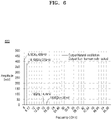
- FIG. 6 illustrates a diagram 600 of a simulation result and depicts a comparison between the frequency spectrum of the output with the proposed solution and with a natural oscillation of the RO unit.
- FIG. 6 illustrates that when a signal of 12GHz is applied and when sub harmonically locked, output frequency locks to 6GHz from a natural oscillation frequency of 6.12GHz. With sub harmonic injection, power at the fundamental harmonic at the output increases by about 20%, and third harmonic power is reduced by 50%.
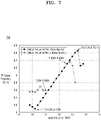
- FIG. 7 illustrates a diagram 700 of a simulation result and depicts the frequency locking range comparison between an existing method and a method according to the inventive concept, with the same applied injection ratio.
- the dotted curve illustrates the frequency locking range achieved by the single phase injection locking techniques and the solid curve illustrates the frequency locking range achieved by the proposed system 104 and method 500.
- Injected signal frequency is swept in the range 9.5 to 14GHz and output frequency is checked. If output frequency is equal to input frequency/2, it is considered to be in locked state.
- the locking range of the single phase injection locking techniques in an example scenario, is 5.5 GHz to 6.6 GHz whereas the locking range of the disclosed system 104 is 5.1 GHz to 6.7 GHz.
- the proposed solution increases the frequency locking range by 100%.
- FIG. 8 illustrates a diagram 800 of a simulation result and depicts IQ Skew comparison between an existing method and the proposed method.
- the dotted curve illustrates the IQ skew achieved by the single phase injection locking techniques and the solid curve illustrates the IQ skew achieved by the disclosed system 104 and method 500.
- the phase interpolator codes are swept to cover phase range of 0 to 180 degrees, this corresponds to 32 codes.
- the spacing between I and Q phases is defined to be 90 degrees at the output frequency. Any deviation from this ideal value is defined as the IQ skew.
- FIG. 8 illustrates that systematic IQ skew with the proposed solution is 10x better than existing methods. This improvement in IQ skew is possible because of the novel simultaneous and symmetric phase injection scheme.
Landscapes
- Physics & Mathematics (AREA)
- Nonlinear Science (AREA)
- Stabilization Of Oscillater, Synchronisation, Frequency Synthesizers (AREA)
Applications Claiming Priority (1)
| Application Number | Priority Date | Filing Date | Title |
|---|---|---|---|
| IN202141004388 | 2021-02-02 |
Publications (1)
| Publication Number | Publication Date |
|---|---|
| EP4037190A1 true EP4037190A1 (fr) | 2022-08-03 |
Family
ID=80121696
Family Applications (1)
| Application Number | Title | Priority Date | Filing Date |
|---|---|---|---|
| EP22153737.6A Pending EP4037190A1 (fr) | 2021-02-02 | 2022-01-27 | Système et procédé de génération de division de fréquence verrouillée sous-harmonique et d'interpolation de phase |
Country Status (2)
| Country | Link |
|---|---|
| US (1) | US11601116B2 (fr) |
| EP (1) | EP4037190A1 (fr) |
Citations (4)
| Publication number | Priority date | Publication date | Assignee | Title |
|---|---|---|---|---|
| WO2011003040A1 (fr) * | 2009-07-01 | 2011-01-06 | Qualcomm Incorporated | Distribution d'oscillateur local à faible puissance à l'aide d'un oscillateur synchronisé par injection de façon sous-harmonique à multiplication de fréquence |
| US20150188554A1 (en) * | 2013-12-31 | 2015-07-02 | Futurewei Technologies, Inc. | Phase Interpolation and Rotation Apparatus and Method |
| US20160308665A1 (en) * | 2014-06-02 | 2016-10-20 | Mediatek Inc. | Method for performing phase shift control for timing recovery in an electronic device, and associated apparatus |
| US10333533B1 (en) * | 2018-09-18 | 2019-06-25 | Cadence Design Systems, Inc. | Hybrid phase interpolator to correct integral non-linearity |
Family Cites Families (13)
| Publication number | Priority date | Publication date | Assignee | Title |
|---|---|---|---|---|
| WO2013006231A2 (fr) | 2011-07-01 | 2013-01-10 | Rambus Inc. | Multiplicateur d'horloge agile en fréquence à faible latence |
| US8674773B2 (en) * | 2012-01-31 | 2014-03-18 | Fujitsu Limited | Phase interpolator with voltage-controlled oscillator injection-lock |
| US8710929B1 (en) | 2012-05-15 | 2014-04-29 | Cadence Design Systems, Inc. | System and method for combined I/Q generation and selective phase interpolation |
| US8810319B1 (en) | 2012-06-08 | 2014-08-19 | Altera Corporation | Dual-stage continuous-time linear equalizer |
| US9444438B2 (en) * | 2013-06-10 | 2016-09-13 | Stmicroelectronics S.R.L. | Frequency doubler and related method of generating an oscillating voltage |
| US9209821B2 (en) | 2014-01-24 | 2015-12-08 | Intel Corporation | Apparatus for generating quadrature clock phases from a single-ended odd-stage ring oscillator |
| GB201406525D0 (en) | 2014-04-11 | 2014-05-28 | Ibm | Continuous, time linear equalizer for high-speed receiving unit |
| US9397623B1 (en) | 2015-02-27 | 2016-07-19 | Huawei Technologies Co., Ltd. | Dual path double zero continuous time linear equalizer |
| US9755574B2 (en) | 2015-08-06 | 2017-09-05 | Sony Corporation | Injection-locked oscillator and method for controlling jitter and/or phase noise |
| US10396807B1 (en) * | 2016-02-08 | 2019-08-27 | Auburn University | Multi-ring coupled ring oscillator with improved phase noise |
| US9735989B1 (en) | 2016-06-23 | 2017-08-15 | Oracle International Corporation | Continuous time linear equalizer that uses cross-coupled cascodes and inductive peaking |
| US10164804B1 (en) | 2017-06-21 | 2018-12-25 | Intel Corporation | Adjusting a continuous time linear equalization-based receiver |
| JP7181470B2 (ja) | 2018-02-08 | 2022-12-01 | 株式会社ソシオネクスト | 加算回路、受信回路及び集積回路 |
-
2021
- 2021-05-04 US US17/307,489 patent/US11601116B2/en active Active
-
2022
- 2022-01-27 EP EP22153737.6A patent/EP4037190A1/fr active Pending
Patent Citations (4)
| Publication number | Priority date | Publication date | Assignee | Title |
|---|---|---|---|---|
| WO2011003040A1 (fr) * | 2009-07-01 | 2011-01-06 | Qualcomm Incorporated | Distribution d'oscillateur local à faible puissance à l'aide d'un oscillateur synchronisé par injection de façon sous-harmonique à multiplication de fréquence |
| US20150188554A1 (en) * | 2013-12-31 | 2015-07-02 | Futurewei Technologies, Inc. | Phase Interpolation and Rotation Apparatus and Method |
| US20160308665A1 (en) * | 2014-06-02 | 2016-10-20 | Mediatek Inc. | Method for performing phase shift control for timing recovery in an electronic device, and associated apparatus |
| US10333533B1 (en) * | 2018-09-18 | 2019-06-25 | Cadence Design Systems, Inc. | Hybrid phase interpolator to correct integral non-linearity |
Non-Patent Citations (2)
| Title |
|---|
| FARAZIAN M ET AL: "Stability and Operation of Injection-Locked Regenerative Frequency Dividers", IEEE TRANSACTIONS ON CIRCUITS AND SYSTEMS I: REGULAR PAPERS, IEEE, US, vol. 57, no. 8, 1 August 2010 (2010-08-01), pages 2006 - 2019, XP011333774, ISSN: 1549-8328, DOI: 10.1109/TCSI.2010.2043012 * |
| SIRIBURANON TEERACHOT ET AL: "A Low-Power Low-Noise mm-Wave Subsampling PLL Using Dual-Step-Mixing ILFD and Tail-Coupling Quadrature Injection-Locked Oscillator for IEEE 802.11ad", IEEE JOURNAL OF SOLID-STATE CIRCUITS, IEEE, USA, vol. 51, no. 5, 1 May 2016 (2016-05-01), pages 1246 - 1260, XP011611626, ISSN: 0018-9200, [retrieved on 20160505], DOI: 10.1109/JSSC.2016.2529004 * |
Also Published As
| Publication number | Publication date |
|---|---|
| US11601116B2 (en) | 2023-03-07 |
| US20220247392A1 (en) | 2022-08-04 |
Similar Documents
| Publication | Publication Date | Title |
|---|---|---|
| US8634509B2 (en) | Synchronized clock phase interpolator | |
| USRE40939E1 (en) | Multi-phase locked loop for data recovery | |
| TWI345368B (en) | Data and clock recovery circuit and gated digital controlled oscillator | |
| US10929102B2 (en) | True random number generator | |
| CN102403043B (zh) | 检测位错误率的电路与系统以及检测抖动容忍度的方法 | |
| US8415996B1 (en) | Clock phase corrector | |
| US7482841B1 (en) | Differential bang-bang phase detector (BBPD) with latency reduction | |
| US9542354B2 (en) | Generating a parallel data signal by converting serial data of a serial data signal to parallel data | |
| US9018996B1 (en) | Circuits, architectures, apparatuses, algorithms and methods for providing quadrature outputs using a plurality of divide-by-n dividers | |
| US8655934B2 (en) | Broadband low noise complex regenerative frequency dividers | |
| US8929467B1 (en) | Circuits and methods for one-wire communication bus of using pulse-edge for clock and pulse-duty-cycle for data | |
| JP2016220038A (ja) | 発振回路、電圧制御発振器、シリアルデータレシーバ | |
| JPH07131448A (ja) | 位相比較回路 | |
| US3636454A (en) | Digital circuit discriminator for frequency-shift data signals | |
| EP4037190A1 (fr) | Système et procédé de génération de division de fréquence verrouillée sous-harmonique et d'interpolation de phase | |
| US7664166B2 (en) | Pleisiochronous repeater system and components thereof | |
| US6259278B1 (en) | Phase detector | |
| Perišić et al. | Time recursive frequency locked loop for the tracking applications | |
| US7378885B1 (en) | Multiphase divider for P-PLL based serial link receivers | |
| CN109150178A (zh) | 一种无电感实现小数正交分频的装置和方法 | |
| US8355478B1 (en) | Circuit for aligning clock to parallel data | |
| US11177932B1 (en) | System for generating multi phase clocks across wide frequency band using tunable passive polyphase filters | |
| US7023944B2 (en) | Method and circuit for glitch-free changing of clocks having different phases | |
| TW201911755A (zh) | 鑒相器及時鐘與數據回復裝置 | |
| US5063577A (en) | High-speed bit synchronizer |
Legal Events
| Date | Code | Title | Description |
|---|---|---|---|
| PUAI | Public reference made under article 153(3) epc to a published international application that has entered the european phase |
Free format text: ORIGINAL CODE: 0009012 |
|
| STAA | Information on the status of an ep patent application or granted ep patent |
Free format text: STATUS: THE APPLICATION HAS BEEN PUBLISHED |
|
| AK | Designated contracting states |
Kind code of ref document: A1 Designated state(s): AL AT BE BG CH CY CZ DE DK EE ES FI FR GB GR HR HU IE IS IT LI LT LU LV MC MK MT NL NO PL PT RO RS SE SI SK SM TR |
|
| STAA | Information on the status of an ep patent application or granted ep patent |
Free format text: STATUS: REQUEST FOR EXAMINATION WAS MADE |
|
| 17P | Request for examination filed |
Effective date: 20230203 |
|
| RBV | Designated contracting states (corrected) |
Designated state(s): AL AT BE BG CH CY CZ DE DK EE ES FI FR GB GR HR HU IE IS IT LI LT LU LV MC MK MT NL NO PL PT RO RS SE SI SK SM TR |
|
| P01 | Opt-out of the competence of the unified patent court (upc) registered |
Effective date: 20230519 |
|
| STAA | Information on the status of an ep patent application or granted ep patent |
Free format text: STATUS: EXAMINATION IS IN PROGRESS |
|
| 17Q | First examination report despatched |
Effective date: 20250415 |