EP4037259B1 - Dispositif amplificateur de ligne destiné à la commande du flux de données - Google Patents
Dispositif amplificateur de ligne destiné à la commande du flux de données Download PDFInfo
- Publication number
- EP4037259B1 EP4037259B1 EP22160668.4A EP22160668A EP4037259B1 EP 4037259 B1 EP4037259 B1 EP 4037259B1 EP 22160668 A EP22160668 A EP 22160668A EP 4037259 B1 EP4037259 B1 EP 4037259B1
- Authority
- EP
- European Patent Office
- Prior art keywords
- interface unit
- line driver
- communication path
- driver device
- ltv
- Prior art date
- Legal status (The legal status is an assumption and is not a legal conclusion. Google has not performed a legal analysis and makes no representation as to the accuracy of the status listed.)
- Active
Links
Images

Classifications
-
- H—ELECTRICITY
- H04—ELECTRIC COMMUNICATION TECHNIQUE
- H04L—TRANSMISSION OF DIGITAL INFORMATION, e.g. TELEGRAPHIC COMMUNICATION
- H04L12/00—Data switching networks
- H04L12/28—Data switching networks characterised by path configuration, e.g. LAN [Local Area Networks] or WAN [Wide Area Networks]
- H04L12/40—Bus networks
-
- H—ELECTRICITY
- H04—ELECTRIC COMMUNICATION TECHNIQUE
- H04L—TRANSMISSION OF DIGITAL INFORMATION, e.g. TELEGRAPHIC COMMUNICATION
- H04L12/00—Data switching networks
- H04L12/28—Data switching networks characterised by path configuration, e.g. LAN [Local Area Networks] or WAN [Wide Area Networks]
- H04L12/40—Bus networks
- H04L12/40006—Architecture of a communication node
-
- H—ELECTRICITY
- H04—ELECTRIC COMMUNICATION TECHNIQUE
- H04L—TRANSMISSION OF DIGITAL INFORMATION, e.g. TELEGRAPHIC COMMUNICATION
- H04L25/00—Baseband systems
- H04L25/02—Details ; arrangements for supplying electrical power along data transmission lines
- H04L25/0264—Arrangements for coupling to transmission lines
- H04L25/0298—Arrangement for terminating transmission lines
Definitions
- the present invention is directed to a line driver device which, for example in a system arrangement for controlling execution units, allows a first or second communication path to be selected for further data flow with little technical effort.
- the proposed line driver device is particularly fault-tolerant and is suitable for use in an automobile, among other things.
- the present invention is also directed to a corresponding system arrangement and to a method for operating or producing the line driver device.
- a computer program product is proposed with control commands which carry out the proposed method or produce or operate the line driver device.
- EN 10 2007 044 820 A1 shows a bus system in a daisy chain arrangement comprising a control unit and a signal transmission device emanating from the control unit with a plurality of bus participants which form a series arrangement along the signal transmission device 5.
- EN 102013201106 A1 shows the data exchange between different components of a technical system.
- the invention relates in particular to the networking and configuration of different components of a technical system in order to enable data exchange between the components.
- DE 100 44 309 A1 shows a redundant data transmission via a data bus in computer networks and an additional line.
- WO 2013/062949 A1 shows a telemetry network with sensors.
- EN 10 2009 056 563 A1 shows a system of bus participants of a bus system for data transmission.
- WO 2017/162 323 A1 shows an efficient control arrangement and a control method, wherein sequentially arranged execution units are controlled by means of a command unit.
- WO 2018/103 880 A1 shows a compact light-emitting diode arrangement which can be used generically, but is particularly advantageous for use in a vehicle due to its compact design.
- WO 2017/153 026 A1 shows a method for brightness compensation in at least one light-emitting diode.
- CAN bus which was developed for cable harnesses and is intended in particular to implement a network of control units.
- ISELED registered trademark
- CAN and LIN the most significant disadvantage of CAN and LIN is that due to the bus architecture, they do not offer any natural (automatic) addressing option. Here, the address must be configured. With ISELED (execution units) and also with the segmented ISELED (line driver unit and execution units) there is a physically predetermined sequence and this results in the possibility of automatically assigning addresses.
- a line driver device should in particular be fail-safe or have no further implications in the event of a failure.
- a system arrangement in which the line driver device is used advantageously.
- a method should be proposed which provides or operates the line driver device.
- a computer program product which has control commands which establish or operate the line driver device and carry out the proposed method.
- a line driver device can be, for example, a device which is provided in a system arrangement and consequently communicates with other line driver devices.
- communication with other components is advantageous, the component being the line driver device which, for example, communicates with several execution units.
- An execution unit is a component that implements instructions that come directly or indirectly from the line driver device.
- An execution device or execution unit can be present as a light-emitting diode unit that controls light-emitting diodes. Light-emitting diodes are typically present as red, green or blue light-emitting diodes, although a white light-emitting diode can also be provided optionally.
- the line driver device thus communicates with several execution units and can itself be set up to receive commands from another unit, for example a command unit.
- a command unit can be a microcontroller
- the line driver device can also be a microcontroller or generally just a unit that provides means for data flow control and also for command processing.
- the line driver device is connected in series, and several such line driver devices are coupled in series along a data line. Consequently, there are typically several line driver devices which are connected to a command unit.
- a first line driver device connected in series is coupled directly to the command unit, the other line driver devices are indirectly coupled to the command unit.
- the failure or inactive state of a line driver device according to the prior art implies that a plurality of other components fail. This is achieved according to the invention by fixed that the proposed line driver device provides a communication path or a data path that simply switches signals in an inactive state.
- the proposed line driver device is fault-tolerant, which is reflected in particular in its interaction with other line driver devices.
- the line driver device itself can already be described as a system arrangement, and thus the terminology relating to the line driver device is also interchangeable in that a system arrangement is already being referred to here.
- the proposed line driver device generally refers to structural features which are only built into the line driver device itself. With regard to external components, the line driver device has the property of communication, which means that the proposed line driver device is not described using external features. Rather, the line driver device is suitable for embedding in a system arrangement which also has other components.
- the line driver device is also efficient because the data flow control is implemented with simple technical means.
- the data flow control only a first communication path and a further communication path are required, as well as two resistors and a switch.
- the data lines or the communication paths can be individual conductor tracks or simply electrical connections. Consequently, the proposed line driver device can be arranged on a simple circuit board or packaged in one piece in a housing.
- the line driver device has at least three interface units for communication with other devices.
- the first interface unit acts as an interface for communication with another line driver device.
- This interface is also suitable for communication with a command unit.
- the command unit is an instance that is higher than the line driver device and provides commands to the line driver device. Consequently, the command unit can act as a master unit with respect to the line driver device, which then acts as a slave unit or client unit.
- the second interface unit can be designed analogously to the first interface unit and is at least suitable for communication with another line driver unit or line driver device.
- the first interface unit can be referred to as an input of the line driver device and the second interface as an output.
- the line driver device can also be coupled bidirectionally to other devices, for example the command device or another line driver device, which also enables bidirectional communication and consequently the second interface unit is present as an input and the first interface unit as an output. Consequently, the two interface units can take on the role of an output or an input depending on the direction of communication.
- the third interface unit is used for communication with execution units, which can be coupled serially, for example.
- the third communication interface or interface unit is used for communication with other external components, with the line driver device behaving as a master unit with respect to these other components.
- the components coupled via the third interface unit can be referred to as execution units, which receive commands and execute them.
- the interface unit it is possible for the interface unit to be designed to receive return values from these execution units.
- a first communication path is arranged between the first interface unit and the second interface unit. This communication path connects both interfaces and is used to transmit signals. Additional components can be arranged on this communication path, which is implemented as a data line, for example, such as at least two resistors or a switch unit. Consequently, the communication path does not have to run continuously from the first interface unit to the second interface unit, but can indirectly transmit data from the first interface unit to the second interface unit, whereby intermediate components can also be installed.
- a second communication path is arranged between the first interface unit, the second interface unit and the third interface unit, which can also connect the interface units directly or indirectly.
- the communication path it is advantageous to design the communication path in such a way that it connects the first interface unit with the third interface unit and then the third interface unit with the second interface unit. Consequently, the second communication path is designed analogously to the first communication path, with the third interface unit also being arranged on the second communication path.
- the second communication path can also comprise further components, such as receiver modules or transmitter modules.
- the second data line or the second communication path it is only one aspect of the present invention that it communicatively couples the first interface unit to the third interface unit and the third interface unit to the second interface unit.
- the arrangement between the interface units can also refer to the fact that a different design is structurally selected, with the logical communication taking place between the proposed interface units.
- a processing unit can be arranged on the second communication path, which processes the incoming signals and then outputs them again.
- the expert will recognize that additional components can be installed for the technical implementation.
- the first communication path has a switch and at least two resistors.
- both resistors are arranged in front of and behind the switch.
- in front of and behind the switch refers to the communication flow, whereby the first communication path can be designed bidirectionally.
- at least one resistor is arranged on both sides of the switch. In general, it can be irrelevant how such a resistor is designed. For example only are suitable for a resistance of 50 ohms. The desired resistance can be created by at least one structural resistor.
- the switch is used to set the communication path, whereby it is generally possible to choose between the first and the second communication path. If a current is applied to the line driver device, data signals are received, the corresponding signals are processed in the internal logic unit and then the processed signals are sent. This corresponds to the second communication path. If, however, no voltage is applied, an analogue transmission takes place, which corresponds to the first communication path. If the installed switch is open, no current flows, and if the switch is closed, current flows. So if the transistor is closed, there is no conducting path. Thus, when it is closed, the first communication path is blocked and the signals are transmitted via the second communication path.
- the switch is open and there is a through path.
- Active through-passing via the second communication path implies data processing, which corresponds to the active state of the line driver device.
- the switch is not directly integrated into the second communication path, but can be supplied with a termination voltage. In general, the switch is always closed and must be actively opened. The line driver device thus switches on if a Voltage is applied. The line driver device is not visible to the other components when no voltage is applied. Consequently, the line driver device switches passively if it fails and still passes signals through passively without affecting other components. No voltage is applied to the line driver device if it is not operating or is broken, and thus signals are passed through passively.
- the third interface unit is set up for communication with execution units that can be connected in series.
- This has the advantage that the interface unit communicates with various execution units, which does not have to be done directly in each case. Rather, it is possible for the plurality of execution units to be connected in series and thus the line driver device preferably communicates directly with a single execution unit via the third interface unit and indirectly with the other connected execution units.
- the third interface unit can transmit commands to the other execution units or receive return values.
- the resistors can be set as pass-through resistors or termination resistors depending on the switch position.
- This has the advantage that the values of the resistors or the individual resistors can be used to set whether the data flow runs via the first communication line or the first communication path or via the second communication line or the second communication path.
- the two resistors are to be added in their effect or not, and this makes it indirectly possible to set the resistance on the data line in such a way that either the first communication path or the second communication path is selected.
- the first communication path and the second communication path are not implemented separately from one another, but rather the communication paths can partially overlap. It is thus possible to provide only one communication line in structural form, with the switch position setting whether the first logical path or the second logical path is selected.
- a logic unit is connected upstream of the third interface unit. This has the advantage that incoming communication signals or commands can be passed through the logic unit via the second communication path and can be processed in the process. Consequently, there is a logic unit on the second communication path which processes signals. The processed signals can then either be output to the execution units via the third interface unit or applied to the output, i.e. the second interface unit.
- the logic unit controls the second interface unit and/or the third interface unit. This has the advantage that either one or two further units can be supplied with the corresponding commands or processed signals. It is thus possible for the logic unit to output a command that is transmitted to the plurality of execution units.
- the switch is coupled between the resistors in the first communication path.
- resistors are located on both sides of the circuit or the switch, with at least one resistor being arranged in each case. In this way, the data flow or the communication path can be advantageously adjusted.
- a termination voltage is applied to the switch.
- the termination voltage corresponds to a maximum of one supply voltage. This has the advantage that the applied voltages are limited and only as much termination voltage needs to be applied as is actually necessary. Here, too, a simple yet efficient structure for data flow control is created.
- the first communication path is a passive communication path.
- the communication path only passes the signals through passively and thus a defective line driver device has no influence on other components.
- the deactivated or defective line driver device does not affect the further communication flow, but rather the signal is passed through via the passive communication path.
- the second communication path is present as an active communication path. This has the advantage that in a normal case, i.e. when the line driver device is operating, the communication path is set to active and the second communication path is then used to process the signals.
- a logic unit can preferably be provided for this purpose.
- the line driver device is formed in one piece. This has the advantage that the line driver device can be installed particularly well in a system arrangement and can, for example, be arranged on a single circuit board or installed in a single housing. The line driver device can thus be provided individually and then installed in further processing steps.
- the switch is in the form of a relay, transistor and/or a digital switch.
- the object is also achieved by a system arrangement with a line driver device as already described.
- a method for efficient and fault-tolerant data flow control comprising providing a first interface unit configured for communication with a command unit or a further line driver device, providing a second interface unit configured to communicate with a further line driver device, providing a third interface unit configured to communicate with a plurality of execution units, wherein a first communication path is arranged between the first interface unit and the second interface unit and a second communication path is arranged between the first interface unit, the second interface unit and the third interface unit, wherein a switch and at least two resistors are arranged on the first communication path and by means of a switch position the data flow is redirected via the first communication path or the second communication path.
- the object is also achieved by a computer program product with control commands which operate the proposed method or operate or produce the proposed line driver device.
- the method provides method steps which can also be functionally reproduced by the structural features of the line driver device.
- the line driver device or the system arrangement provide structural features which are suitable for carrying out the method.
- Fig.1 shows a microcontroller on the left, which acts as a command unit, for example.
- several execution units are arranged using bidirectional communication, which are implemented here as LED controllers. This is shown by the reference symbol MLED CTRL.
- MLED CTRL the reference symbol
- Fig.1 shows a possible design of a system or communication arrangement according to the state of the art.
- the command unit BE can be seen on the left side, which is connected to three control units. Since the three control units are connected in series, the command unit is directly connected to one control unit and indirectly connected to the other control units.
- the control units can be so-called multi-LED controllers. This is the case in the present Fig.1 as MLED CTRL.
- the uniform reference symbol is intended to make it clear in particular that the control units are typically designed in the same way.
- the light-emitting diodes are RGB (red, green, blue) light-emitting diodes.
- the data line is present as a plurality of data line segments, which are shown as bidirectional arrows SIO1, SIO2.
- Control units can also be referred to as execution units.
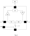
- Fig. 2 shows the line driver device LTV according to the invention.
- three interface units are provided, namely the first interface unit A, the second interface unit B and the third interface unit C.
- a logic unit LE is also connected upstream of the third interface unit C.
- the third interface unit C is set up to communicate with a large number of further execution units AE.
- further components can be installed, such as a receiver Rx and a transmitter Tx.
- R stands for receiver and T for transmitter.
- the resistors W1, W2 are also shown, as is the switch S.
- a current source or voltage source VCC is also shown on the bottom left.
- the first communication path is shown with a dashed line and connects the first interface unit with the second interface unit B. This is done indirectly, with several components such as the first resistor W1 and the second resistor W2 being arranged in between.
- the switch S is also arranged on the first data line.
- the second data line is shown with the dotted line and runs between the first interface unit A, the second interface unit B via the third interface unit C.
- the logic unit LE which is also located on the second data line, is connected upstream of the third interface unit.
- the first data line i.e. the dashed data line
- the second data line i.e. the dotted data line
- the first data line and the second data line can be designed in such a way that at least the first section is implemented together, i.e. that a single data line is arranged between the interface unit A and the resistor W1, and a single data line is arranged between the second resistor W2 and the second interface unit B. Both the first communication path and the second communication path are then coupled into this data line.
- the corresponding signals then flow either horizontally from the first interface unit A via the at least one resistor or the switch to the second interface unit B.
- the second data line can also be selected, which then runs via the third interface unit C.
- Further line driver devices LTV can be arranged either on the left and/or on the right, and thus they can communicate via the interface units A or B. It is also possible that in the present Fig. 2 above, several execution units AE are provided, which are connected in series.
- the system arrangement proposed according to the invention can therefore comprise not just one line driver device LTV, but several which are connected in series, as well as several execution units AE which are also to be connected in series.
- a command unit can be provided which communicates with the line driver device LTV, for example, via the interface A.
- Such a command unit can be implemented as a microcontroller.
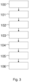
- Fig.3 shows in a schematic flow diagram the proposed method for efficient and fault-tolerant data flow control, comprising providing 100 a first interface unit A set up for communication with a command unit BE or a further line driver device LTV.
- Providing 101 a second interface unit B set up for communication with a further line driver device LTV, providing 102 a third interface unit C set up for communication with a multiplicity of execution units AE, wherein a first communication path is arranged 103 between the first interface unit A and the second interface unit B and a second communication path is arranged 104 between the first interface unit A, the second interface unit B and the third interface unit C, wherein a switch S and at least two resistors W1, W2 are arranged 105 on the first communication path and by means of a switch position the data flow is redirected 106 via the first communication path or the second communication path.
Landscapes
- Engineering & Computer Science (AREA)
- Computer Networks & Wireless Communication (AREA)
- Signal Processing (AREA)
- Power Engineering (AREA)
- Dc Digital Transmission (AREA)
- Small-Scale Networks (AREA)
- Safety Devices In Control Systems (AREA)
Claims (13)
- Dispositif de commande de ligne (LTV) pour un contrôle de flux de données efficace et tolérant aux pannes, comprenant :- une première unité d'interface (A) agencée pour communiquer avec une unité de commande ou un autre dispositif de commande de ligne (LTV);- une seconde unité d'interface (B) agencée pour communiquer avec un autre dispositif de commande de ligne (LTV);- une troisième unité d'interface (C) agencée pour communiquer avec une pluralité d'unités d'exécution (AE), caractérisée en ce qu'un premier chemin de communication est disposé entre la première unité d'interface (A) et la deuxième unité d'interface (B) et un deuxième chemin de communication est disposé entre la première unité d'interface (A) et la deuxième unité d'interface (B). Un deuxième chemin de communication est disposé entre l'unité d'interface (A), la deuxième unité d'interface (B) et la troisième unité d'interface (C), un commutateur (S) et au moins deux résistances (W1, W2) étant disposés sur le premier chemin de communication et, au moyen d'une position du commutateur, le flux de données étant transmis par le biais du deuxième chemin de communication. De communication ou le deuxième chemin de communication et, en fonction de la position du commutateur, les résistances (W1, W2) peuvent être réglées comme résistances de passage ou résistances de termi- nisation et une tension de terminaison est appliquée au commutateur (S).
- Dispositif de commande de ligne (LTV) selon la revendication 1, caractérisé en ce que la troisième unité d'interface (C) est conçue pour communiquer avec des unités d'exécution (AE) pouvant être connectées en série.
- Dispositif de commande de ligne (LTV) selon l'une des revendications précédentes, caractérisé en ce qu'une unité logique (LE) est montée en amont de la troisième unité d'interface (C).
- Dispositif de commande de ligne (LTV) selon la revendication 4, caractérisé en ce que l'unité logique (LE) commande la deuxième unité d'interface (B) et/ou la troisième unité d'interface (C)
- Dispositif d'attaque de ligne (LTV) selon l'un des précédents revendications, caractérisé en ce que le commutateur (S) est couplé entre les résistances (Wh W2) dans le premier chemin de communication.
- Dispositif d'attaque de ligne (LTV) selon l'un des précédents revendications, caractérisé en ce que la tension de terminaison correspond au maximum à une tension d'alimentation
- Dispositif de commande de ligne (LTV) selon l'une quelconque des revendications précédentes, caractérisé en ce que le premier circuit de communication est un circuit de commande de ligne. Qu'une voie de communication passive.
- Dispositif de commande de ligne (LTV) selon l'une quelconque des revendications précédentes, caractérisé en ce que le deuxième chemin de communication est un chemin de communication actif.
- Dispositif de commande de ligne (LTV) selon l'une des revendications précédentes, caractérisé en ce que le dispositif de commande de ligne (LTV) est formé d'une seule pièce.
- Dispositif d'attaque de ligne (LTV) selon l'une quelconque des revendications précédentes, caractérisé en ce que le commutateur (S) se présente sous la forme d'un RELIS, d'un transistor et/ou d'un commutateur numérique.
- Agencement du système avec un dispositif de commande de ligne (LTV) selon ei-l'une des revendications précédentes.
- Méthode de contrôle de flux de données efficace et tolérante aux pannes, comprenant:- fournir (100) une première unité d'interface (A) adaptée pour communiquer avec une unité de commande ou un autre dispositif de commande de ligne (LTV);- fournir (101) une deuxième unité d'interface (B) agencée pour communiquer avec un autre dispositif de commande de ligne, et de l'assurance maladie (LTV);- fournir (102) une troisième unité d'interface (C) agencée pour communiquer avec une pluralité d'unités d'exécution (AE), caractérisée en ce que, entre la première unité d'interface (A) et la deuxième unité d'interface (B), la troisième unité d'interface (C) est agencée pour communiquer avec une pluralité d'unités d'exécution (AE). Un premier chemin de communication est disposé (103) et un deuxième chemin de communication est disposé (104) entre la première unité d'interface (A), la deuxième unité d'interface (B) et la troisième unité d'interface (C), dans lequel un commutateur est disposé (105) entre la première unité d'interface (A) et la deuxième unité d'interface (B) et au moins deux résistances (W1, W2) sur le premier de communication (105) et, au moyen d'une position de commutation, le flux de données est dévié (106) par l'intermédiaire du premier chemin de communication ou du deuxième chemin de communication, les résistances(Wh W2) sont réglées comme résistances de passage ou résistances de terminaison et une tension de termi- nisation est appliquée au commutateur (S).
- Produit de programme d'ordinateur comprenant des instructions de commande qui, lorsqu'elles sont exécutées sur un ordinateur, exécutent le procédé selon la revendication 12.
Applications Claiming Priority (4)
| Application Number | Priority Date | Filing Date | Title |
|---|---|---|---|
| DE102018007144.9A DE102018007144B4 (de) | 2018-09-10 | 2018-09-10 | Leitungstreibervorrichtung zur Datenflusskontrolle |
| EP19733398.2A EP3834388B1 (fr) | 2018-09-10 | 2019-06-17 | Dispositif de commande de ligne pour le contrôle de flux de données |
| EP21199639.2A EP3982595B1 (fr) | 2018-09-10 | 2019-06-17 | Dispositif amplificateur de ligne destiné à la vérification du flux de données |
| PCT/EP2019/025187 WO2020052802A1 (fr) | 2018-09-10 | 2019-06-17 | Dispositif de commande de ligne pour le contrôle de flux de données |
Related Parent Applications (4)
| Application Number | Title | Priority Date | Filing Date |
|---|---|---|---|
| EP21199639.2A Division-Into EP3982595B1 (fr) | 2018-09-10 | 2019-06-17 | Dispositif amplificateur de ligne destiné à la vérification du flux de données |
| EP21199639.2A Division EP3982595B1 (fr) | 2018-09-10 | 2019-06-17 | Dispositif amplificateur de ligne destiné à la vérification du flux de données |
| EP21199639.2A Previously-Filed-Application EP3982595B1 (fr) | 2018-09-10 | 2019-06-17 | Dispositif amplificateur de ligne destiné à la vérification du flux de données |
| EP19733398.2A Division EP3834388B1 (fr) | 2018-09-10 | 2019-06-17 | Dispositif de commande de ligne pour le contrôle de flux de données |
Publications (2)
| Publication Number | Publication Date |
|---|---|
| EP4037259A1 EP4037259A1 (fr) | 2022-08-03 |
| EP4037259B1 true EP4037259B1 (fr) | 2024-07-31 |
Family
ID=67060359
Family Applications (3)
| Application Number | Title | Priority Date | Filing Date |
|---|---|---|---|
| EP21199639.2A Active EP3982595B1 (fr) | 2018-09-10 | 2019-06-17 | Dispositif amplificateur de ligne destiné à la vérification du flux de données |
| EP19733398.2A Active EP3834388B1 (fr) | 2018-09-10 | 2019-06-17 | Dispositif de commande de ligne pour le contrôle de flux de données |
| EP22160668.4A Active EP4037259B1 (fr) | 2018-09-10 | 2019-06-17 | Dispositif amplificateur de ligne destiné à la commande du flux de données |
Family Applications Before (2)
| Application Number | Title | Priority Date | Filing Date |
|---|---|---|---|
| EP21199639.2A Active EP3982595B1 (fr) | 2018-09-10 | 2019-06-17 | Dispositif amplificateur de ligne destiné à la vérification du flux de données |
| EP19733398.2A Active EP3834388B1 (fr) | 2018-09-10 | 2019-06-17 | Dispositif de commande de ligne pour le contrôle de flux de données |
Country Status (8)
| Country | Link |
|---|---|
| EP (3) | EP3982595B1 (fr) |
| JP (1) | JP6996806B2 (fr) |
| KR (1) | KR102294548B1 (fr) |
| CN (1) | CN112771822B (fr) |
| DE (1) | DE102018007144B4 (fr) |
| ES (3) | ES2900076T3 (fr) |
| SG (1) | SG11202102331SA (fr) |
| WO (1) | WO2020052802A1 (fr) |
Families Citing this family (1)
| Publication number | Priority date | Publication date | Assignee | Title |
|---|---|---|---|---|
| ES3009477T3 (en) | 2021-03-17 | 2025-03-27 | Inova Semiconductors Gmbh | Low latency command propagation protocol |
Family Cites Families (22)
| Publication number | Priority date | Publication date | Assignee | Title |
|---|---|---|---|---|
| JPH01114133A (ja) * | 1987-10-27 | 1989-05-02 | Fujitsu Ltd | 信号伝送回路 |
| JPH06327007A (ja) * | 1993-05-12 | 1994-11-25 | Matsushita Electric Ind Co Ltd | Avネットワークシステム |
| JPH09107277A (ja) * | 1995-10-13 | 1997-04-22 | Nec Eng Ltd | 波形整形回路 |
| DE19916635C1 (de) * | 1999-04-13 | 2001-01-25 | Siemens Ag | Verfahren und Vorrichtung zum Übertragen eines Sendesignals über eine zweiadrige Leitung |
| DE10044309A1 (de) * | 2000-09-07 | 2002-04-04 | Ean Elektroschaltanlagen Gmbh | Redundante Datenübertragung über Datenbus |
| CN201026897Y (zh) * | 2007-04-18 | 2008-02-27 | 北京康吉森交通技术有限公司 | 模块化计算机联锁信号模块 |
| DE102007044820B4 (de) * | 2007-09-20 | 2009-06-18 | Insta Elektro Gmbh | Bussystem und Verfahren für dessen Betrieb |
| DE102009056563B4 (de) * | 2009-12-03 | 2011-12-29 | Sew-Eurodrive Gmbh & Co. Kg | System von Busteilnehmern eines Bussystems zur Datenübertragung |
| DE102010029300A1 (de) * | 2010-05-26 | 2011-05-19 | Siemens Aktiengesellschaft | Netzwerkschnittstelle und Verfahren zur Datenübertragung |
| WO2013062949A1 (fr) * | 2011-10-25 | 2013-05-02 | Martin Scientific, Llc | Réseau de capteurs et de télémesure de fond de trou à haut débit |
| US8760198B2 (en) * | 2011-12-27 | 2014-06-24 | Broadcom Corporation | Low voltage line driver |
| EP2631806A1 (fr) * | 2012-02-27 | 2013-08-28 | Televic Rail NV | Dispositifs et procédé pour attribuer des adresses de réseau |
| DE102013201106B4 (de) * | 2013-01-24 | 2014-12-11 | Smiths Heimann Gmbh | Busknoten und Bussystem sowie Verfahren zur Identifikation der Busknoten des Bussystems |
| DE202013103146U1 (de) * | 2013-07-15 | 2014-10-16 | Hanning & Kahl Gmbh & Co. Kg | Gerätesystem |
| US9112550B1 (en) * | 2014-06-25 | 2015-08-18 | Kandou Labs, SA | Multilevel driver for high speed chip-to-chip communications |
| DE102015111465A1 (de) | 2015-07-15 | 2017-01-19 | Inova Semiconductors Gmbh | Verfahren, Vorrichtung und System zum empfängerseitigen Bestimmen eines Abtastzeitpunkts |
| US10484202B2 (en) * | 2015-11-05 | 2019-11-19 | Hitachi Automotive Systems, Ltd. | Relay device, electronic control device, and vehicle-mounted network system |
| DE102016104440B4 (de) | 2016-03-10 | 2025-10-02 | Inova Semiconductors Gmbh | Verfahren und Vorrichtung zur Helligkeitskompensation einer LED |
| DE102016105264B4 (de) | 2016-03-21 | 2017-11-23 | Inova Semiconductors Gmbh | Effiziente Steuerungsanordnung und Steuerungsverfahren |
| US9887737B2 (en) * | 2016-04-25 | 2018-02-06 | Cisco Technology, Inc. | Radio frequency signal fault signature isolation in cable network environments |
| DE102016014649A1 (de) | 2016-12-08 | 2018-06-14 | Inova Semiconductors Gmbh | Kompakte Leuchtdioden-Anordnung |
| DE102017208833B4 (de) * | 2017-05-24 | 2018-12-13 | Wago Verwaltungsgesellschaft Mbh | Moduleinheit |
-
2018
- 2018-09-10 DE DE102018007144.9A patent/DE102018007144B4/de active Active
-
2019
- 2019-06-17 ES ES19733398T patent/ES2900076T3/es active Active
- 2019-06-17 CN CN201980059100.2A patent/CN112771822B/zh active Active
- 2019-06-17 EP EP21199639.2A patent/EP3982595B1/fr active Active
- 2019-06-17 SG SG11202102331SA patent/SG11202102331SA/en unknown
- 2019-06-17 ES ES21199639T patent/ES2990965T3/es active Active
- 2019-06-17 KR KR1020217006928A patent/KR102294548B1/ko active Active
- 2019-06-17 EP EP19733398.2A patent/EP3834388B1/fr active Active
- 2019-06-17 ES ES22160668T patent/ES2991389T3/es active Active
- 2019-06-17 WO PCT/EP2019/025187 patent/WO2020052802A1/fr not_active Ceased
- 2019-06-17 JP JP2021512846A patent/JP6996806B2/ja active Active
- 2019-06-17 EP EP22160668.4A patent/EP4037259B1/fr active Active
Also Published As
| Publication number | Publication date |
|---|---|
| JP2021527372A (ja) | 2021-10-11 |
| ES2990965T3 (es) | 2024-12-02 |
| EP3982595A9 (fr) | 2023-01-11 |
| WO2020052802A1 (fr) | 2020-03-19 |
| SG11202102331SA (en) | 2021-04-29 |
| CN112771822B (zh) | 2022-04-19 |
| EP3982595B1 (fr) | 2024-07-31 |
| KR20210030996A (ko) | 2021-03-18 |
| DE102018007144A1 (de) | 2019-08-29 |
| ES2991389T3 (es) | 2024-12-03 |
| KR102294548B1 (ko) | 2021-08-26 |
| EP3834388A1 (fr) | 2021-06-16 |
| EP3982595A1 (fr) | 2022-04-13 |
| DE102018007144B4 (de) | 2019-10-10 |
| JP6996806B2 (ja) | 2022-02-03 |
| ES2900076T3 (es) | 2022-03-15 |
| CN112771822A (zh) | 2021-05-07 |
| EP3834388B1 (fr) | 2021-11-10 |
| EP4037259A1 (fr) | 2022-08-03 |
Similar Documents
| Publication | Publication Date | Title |
|---|---|---|
| EP4236631B1 (fr) | Agencement de commande segmenté | |
| DE19928517A1 (de) | Steuerungssystem zum Steuern von sicherheitskritischen Prozessen | |
| DE102016000126A1 (de) | Serielles Bussystem mit Koppelmodulen | |
| DE102021104422A1 (de) | Verfahren zum Betreiben eines Kommunikationssystems, Kommunikationssystem und Rechensystem | |
| EP4037259B1 (fr) | Dispositif amplificateur de ligne destiné à la commande du flux de données | |
| EP3834378B1 (fr) | Dispositif de commande de ligne efficace pour le contrôle de flux de données | |
| DE102018010310B3 (de) | Effiziente Leitungstreibervorrichtung zur Datenflusskontrolle | |
| DE102018010311B3 (de) | Effiziente Leitungstreibervorrichtung zur Datenflusskontrolle | |
| DE102018010305C5 (de) | Segmentierte Steuerungsanordnung | |
| EP1898551B1 (fr) | Appareil comprenant un interface système | |
| DE202018006224U1 (de) | Effiziente Leitungstreibervorrichtung zur Datenflusskontrolle | |
| DE102018010307B4 (de) | Segmentierte Steuerungsanordnung |
Legal Events
| Date | Code | Title | Description |
|---|---|---|---|
| PUAI | Public reference made under article 153(3) epc to a published international application that has entered the european phase |
Free format text: ORIGINAL CODE: 0009012 |
|
| STAA | Information on the status of an ep patent application or granted ep patent |
Free format text: STATUS: REQUEST FOR EXAMINATION WAS MADE |
|
| 17P | Request for examination filed |
Effective date: 20220330 |
|
| AC | Divisional application: reference to earlier application |
Ref document number: 3834388 Country of ref document: EP Kind code of ref document: P Ref document number: 3982595 Country of ref document: EP Kind code of ref document: P |
|
| AK | Designated contracting states |
Kind code of ref document: A1 Designated state(s): AL AT BE BG CH CY CZ DE DK EE ES FI FR GB GR HR HU IE IS IT LI LT LU LV MC MK MT NL NO PL PT RO RS SE SI SK SM TR |
|
| STAA | Information on the status of an ep patent application or granted ep patent |
Free format text: STATUS: EXAMINATION IS IN PROGRESS |
|
| 17Q | First examination report despatched |
Effective date: 20230203 |
|
| GRAP | Despatch of communication of intention to grant a patent |
Free format text: ORIGINAL CODE: EPIDOSNIGR1 |
|
| STAA | Information on the status of an ep patent application or granted ep patent |
Free format text: STATUS: GRANT OF PATENT IS INTENDED |
|
| INTG | Intention to grant announced |
Effective date: 20240229 |
|
| GRAS | Grant fee paid |
Free format text: ORIGINAL CODE: EPIDOSNIGR3 |
|
| GRAA | (expected) grant |
Free format text: ORIGINAL CODE: 0009210 |
|
| STAA | Information on the status of an ep patent application or granted ep patent |
Free format text: STATUS: THE PATENT HAS BEEN GRANTED |
|
| AC | Divisional application: reference to earlier application |
Ref document number: 3834388 Country of ref document: EP Kind code of ref document: P Ref document number: 3982595 Country of ref document: EP Kind code of ref document: P |
|
| AK | Designated contracting states |
Kind code of ref document: B1 Designated state(s): AL AT BE BG CH CY CZ DE DK EE ES FI FR GB GR HR HU IE IS IT LI LT LU LV MC MK MT NL NO PL PT RO RS SE SI SK SM TR |
|
| REG | Reference to a national code |
Ref country code: CH Ref legal event code: EP Ref country code: GB Ref legal event code: FG4D Free format text: NOT ENGLISH |
|
| REG | Reference to a national code |
Ref country code: DE Ref legal event code: R096 Ref document number: 502019011813 Country of ref document: DE |
|
| REG | Reference to a national code |
Ref country code: IE Ref legal event code: FG4D Free format text: LANGUAGE OF EP DOCUMENT: GERMAN |
|
| REG | Reference to a national code |
Ref country code: NL Ref legal event code: FP |
|
| P01 | Opt-out of the competence of the unified patent court (upc) registered |
Free format text: CASE NUMBER: APP_51382/2024 Effective date: 20240911 |
|
| REG | Reference to a national code |
Ref country code: SE Ref legal event code: TRGR |
|
| REG | Reference to a national code |
Ref country code: LT Ref legal event code: MG9D |
|
| REG | Reference to a national code |
Ref country code: ES Ref legal event code: FG2A Ref document number: 2991389 Country of ref document: ES Kind code of ref document: T3 Effective date: 20241203 |
|
| PG25 | Lapsed in a contracting state [announced via postgrant information from national office to epo] |
Ref country code: PT Free format text: LAPSE BECAUSE OF FAILURE TO SUBMIT A TRANSLATION OF THE DESCRIPTION OR TO PAY THE FEE WITHIN THE PRESCRIBED TIME-LIMIT Effective date: 20241202 |
|
| PG25 | Lapsed in a contracting state [announced via postgrant information from national office to epo] |
Ref country code: PT Free format text: LAPSE BECAUSE OF FAILURE TO SUBMIT A TRANSLATION OF THE DESCRIPTION OR TO PAY THE FEE WITHIN THE PRESCRIBED TIME-LIMIT Effective date: 20241202 |
|
| PG25 | Lapsed in a contracting state [announced via postgrant information from national office to epo] |
Ref country code: NO Free format text: LAPSE BECAUSE OF FAILURE TO SUBMIT A TRANSLATION OF THE DESCRIPTION OR TO PAY THE FEE WITHIN THE PRESCRIBED TIME-LIMIT Effective date: 20241031 |
|
| PG25 | Lapsed in a contracting state [announced via postgrant information from national office to epo] |
Ref country code: FI Free format text: LAPSE BECAUSE OF FAILURE TO SUBMIT A TRANSLATION OF THE DESCRIPTION OR TO PAY THE FEE WITHIN THE PRESCRIBED TIME-LIMIT Effective date: 20240731 Ref country code: PL Free format text: LAPSE BECAUSE OF FAILURE TO SUBMIT A TRANSLATION OF THE DESCRIPTION OR TO PAY THE FEE WITHIN THE PRESCRIBED TIME-LIMIT Effective date: 20240731 Ref country code: GR Free format text: LAPSE BECAUSE OF FAILURE TO SUBMIT A TRANSLATION OF THE DESCRIPTION OR TO PAY THE FEE WITHIN THE PRESCRIBED TIME-LIMIT Effective date: 20241101 |
|
| PG25 | Lapsed in a contracting state [announced via postgrant information from national office to epo] |
Ref country code: BG Free format text: LAPSE BECAUSE OF FAILURE TO SUBMIT A TRANSLATION OF THE DESCRIPTION OR TO PAY THE FEE WITHIN THE PRESCRIBED TIME-LIMIT Effective date: 20240731 |
|
| PG25 | Lapsed in a contracting state [announced via postgrant information from national office to epo] |
Ref country code: LV Free format text: LAPSE BECAUSE OF FAILURE TO SUBMIT A TRANSLATION OF THE DESCRIPTION OR TO PAY THE FEE WITHIN THE PRESCRIBED TIME-LIMIT Effective date: 20240731 |
|
| PG25 | Lapsed in a contracting state [announced via postgrant information from national office to epo] |
Ref country code: IS Free format text: LAPSE BECAUSE OF FAILURE TO SUBMIT A TRANSLATION OF THE DESCRIPTION OR TO PAY THE FEE WITHIN THE PRESCRIBED TIME-LIMIT Effective date: 20241130 |
|
| PG25 | Lapsed in a contracting state [announced via postgrant information from national office to epo] |
Ref country code: HR Free format text: LAPSE BECAUSE OF FAILURE TO SUBMIT A TRANSLATION OF THE DESCRIPTION OR TO PAY THE FEE WITHIN THE PRESCRIBED TIME-LIMIT Effective date: 20240731 |
|
| PG25 | Lapsed in a contracting state [announced via postgrant information from national office to epo] |
Ref country code: RS Free format text: LAPSE BECAUSE OF FAILURE TO SUBMIT A TRANSLATION OF THE DESCRIPTION OR TO PAY THE FEE WITHIN THE PRESCRIBED TIME-LIMIT Effective date: 20241031 |
|
| PG25 | Lapsed in a contracting state [announced via postgrant information from national office to epo] |
Ref country code: RS Free format text: LAPSE BECAUSE OF FAILURE TO SUBMIT A TRANSLATION OF THE DESCRIPTION OR TO PAY THE FEE WITHIN THE PRESCRIBED TIME-LIMIT Effective date: 20241031 Ref country code: PL Free format text: LAPSE BECAUSE OF FAILURE TO SUBMIT A TRANSLATION OF THE DESCRIPTION OR TO PAY THE FEE WITHIN THE PRESCRIBED TIME-LIMIT Effective date: 20240731 Ref country code: NO Free format text: LAPSE BECAUSE OF FAILURE TO SUBMIT A TRANSLATION OF THE DESCRIPTION OR TO PAY THE FEE WITHIN THE PRESCRIBED TIME-LIMIT Effective date: 20241031 Ref country code: LV Free format text: LAPSE BECAUSE OF FAILURE TO SUBMIT A TRANSLATION OF THE DESCRIPTION OR TO PAY THE FEE WITHIN THE PRESCRIBED TIME-LIMIT Effective date: 20240731 Ref country code: IS Free format text: LAPSE BECAUSE OF FAILURE TO SUBMIT A TRANSLATION OF THE DESCRIPTION OR TO PAY THE FEE WITHIN THE PRESCRIBED TIME-LIMIT Effective date: 20241130 Ref country code: HR Free format text: LAPSE BECAUSE OF FAILURE TO SUBMIT A TRANSLATION OF THE DESCRIPTION OR TO PAY THE FEE WITHIN THE PRESCRIBED TIME-LIMIT Effective date: 20240731 Ref country code: GR Free format text: LAPSE BECAUSE OF FAILURE TO SUBMIT A TRANSLATION OF THE DESCRIPTION OR TO PAY THE FEE WITHIN THE PRESCRIBED TIME-LIMIT Effective date: 20241101 Ref country code: FI Free format text: LAPSE BECAUSE OF FAILURE TO SUBMIT A TRANSLATION OF THE DESCRIPTION OR TO PAY THE FEE WITHIN THE PRESCRIBED TIME-LIMIT Effective date: 20240731 Ref country code: BG Free format text: LAPSE BECAUSE OF FAILURE TO SUBMIT A TRANSLATION OF THE DESCRIPTION OR TO PAY THE FEE WITHIN THE PRESCRIBED TIME-LIMIT Effective date: 20240731 |
|
| PG25 | Lapsed in a contracting state [announced via postgrant information from national office to epo] |
Ref country code: SM Free format text: LAPSE BECAUSE OF FAILURE TO SUBMIT A TRANSLATION OF THE DESCRIPTION OR TO PAY THE FEE WITHIN THE PRESCRIBED TIME-LIMIT Effective date: 20240731 Ref country code: DK Free format text: LAPSE BECAUSE OF FAILURE TO SUBMIT A TRANSLATION OF THE DESCRIPTION OR TO PAY THE FEE WITHIN THE PRESCRIBED TIME-LIMIT Effective date: 20240731 Ref country code: RO Free format text: LAPSE BECAUSE OF FAILURE TO SUBMIT A TRANSLATION OF THE DESCRIPTION OR TO PAY THE FEE WITHIN THE PRESCRIBED TIME-LIMIT Effective date: 20240731 |
|
| PG25 | Lapsed in a contracting state [announced via postgrant information from national office to epo] |
Ref country code: EE Free format text: LAPSE BECAUSE OF FAILURE TO SUBMIT A TRANSLATION OF THE DESCRIPTION OR TO PAY THE FEE WITHIN THE PRESCRIBED TIME-LIMIT Effective date: 20240731 |
|
| PG25 | Lapsed in a contracting state [announced via postgrant information from national office to epo] |
Ref country code: CZ Free format text: LAPSE BECAUSE OF FAILURE TO SUBMIT A TRANSLATION OF THE DESCRIPTION OR TO PAY THE FEE WITHIN THE PRESCRIBED TIME-LIMIT Effective date: 20240731 |
|
| PG25 | Lapsed in a contracting state [announced via postgrant information from national office to epo] |
Ref country code: SK Free format text: LAPSE BECAUSE OF FAILURE TO SUBMIT A TRANSLATION OF THE DESCRIPTION OR TO PAY THE FEE WITHIN THE PRESCRIBED TIME-LIMIT Effective date: 20240731 |
|
| REG | Reference to a national code |
Ref country code: DE Ref legal event code: R097 Ref document number: 502019011813 Country of ref document: DE |
|
| PLBE | No opposition filed within time limit |
Free format text: ORIGINAL CODE: 0009261 |
|
| STAA | Information on the status of an ep patent application or granted ep patent |
Free format text: STATUS: NO OPPOSITION FILED WITHIN TIME LIMIT |
|
| 26N | No opposition filed |
Effective date: 20250501 |
|
| PGFP | Annual fee paid to national office [announced via postgrant information from national office to epo] |
Ref country code: DE Payment date: 20250618 Year of fee payment: 7 |
|
| PGFP | Annual fee paid to national office [announced via postgrant information from national office to epo] |
Ref country code: GB Payment date: 20250620 Year of fee payment: 7 |
|
| PGFP | Annual fee paid to national office [announced via postgrant information from national office to epo] |
Ref country code: NL Payment date: 20250618 Year of fee payment: 7 |
|
| PGFP | Annual fee paid to national office [announced via postgrant information from national office to epo] |
Ref country code: FR Payment date: 20250627 Year of fee payment: 7 |
|
| PGFP | Annual fee paid to national office [announced via postgrant information from national office to epo] |
Ref country code: SE Payment date: 20250618 Year of fee payment: 7 |
|
| PGFP | Annual fee paid to national office [announced via postgrant information from national office to epo] |
Ref country code: ES Payment date: 20250718 Year of fee payment: 7 |
|
| PGFP | Annual fee paid to national office [announced via postgrant information from national office to epo] |
Ref country code: IT Payment date: 20250630 Year of fee payment: 7 |
|
| REG | Reference to a national code |
Ref country code: CH Ref legal event code: H13 Free format text: ST27 STATUS EVENT CODE: U-0-0-H10-H13 (AS PROVIDED BY THE NATIONAL OFFICE) Effective date: 20260127 |
|
| PG25 | Lapsed in a contracting state [announced via postgrant information from national office to epo] |
Ref country code: MC Free format text: LAPSE BECAUSE OF FAILURE TO SUBMIT A TRANSLATION OF THE DESCRIPTION OR TO PAY THE FEE WITHIN THE PRESCRIBED TIME-LIMIT Effective date: 20240731 |
|
| PG25 | Lapsed in a contracting state [announced via postgrant information from national office to epo] |
Ref country code: LU Free format text: LAPSE BECAUSE OF NON-PAYMENT OF DUE FEES Effective date: 20250617 |
|
| REG | Reference to a national code |
Ref country code: BE Ref legal event code: MM Effective date: 20250630 |
|
| PG25 | Lapsed in a contracting state [announced via postgrant information from national office to epo] |
Ref country code: IE Free format text: LAPSE BECAUSE OF NON-PAYMENT OF DUE FEES Effective date: 20250617 |
|
| PG25 | Lapsed in a contracting state [announced via postgrant information from national office to epo] |
Ref country code: BE Free format text: LAPSE BECAUSE OF NON-PAYMENT OF DUE FEES Effective date: 20250630 |