EP4040502A1 - Verfahren zur herstellung eines halbleiterbauelements sowie halbleiterbauelement - Google Patents
Verfahren zur herstellung eines halbleiterbauelements sowie halbleiterbauelement Download PDFInfo
- Publication number
- EP4040502A1 EP4040502A1 EP22155142.7A EP22155142A EP4040502A1 EP 4040502 A1 EP4040502 A1 EP 4040502A1 EP 22155142 A EP22155142 A EP 22155142A EP 4040502 A1 EP4040502 A1 EP 4040502A1
- Authority
- EP
- European Patent Office
- Prior art keywords
- hard mask
- semiconductor device
- region
- semiconductor base
- ion
- Prior art date
- Legal status (The legal status is an assumption and is not a legal conclusion. Google has not performed a legal analysis and makes no representation as to the accuracy of the status listed.)
- Withdrawn
Links
Images


Classifications
-
- H—ELECTRICITY
- H10—SEMICONDUCTOR DEVICES; ELECTRIC SOLID-STATE DEVICES NOT OTHERWISE PROVIDED FOR
- H10D—INORGANIC ELECTRIC SEMICONDUCTOR DEVICES
- H10D12/00—Bipolar devices controlled by the field effect, e.g. insulated-gate bipolar transistors [IGBT]
- H10D12/01—Manufacture or treatment
- H10D12/031—Manufacture or treatment of IGBTs
-
- H—ELECTRICITY
- H10—SEMICONDUCTOR DEVICES; ELECTRIC SOLID-STATE DEVICES NOT OTHERWISE PROVIDED FOR
- H10P—GENERIC PROCESSES OR APPARATUS FOR THE MANUFACTURE OR TREATMENT OF DEVICES COVERED BY CLASS H10
- H10P30/00—Ion implantation into wafers, substrates or parts of devices
- H10P30/20—Ion implantation into wafers, substrates or parts of devices into semiconductor materials, e.g. for doping
- H10P30/22—Ion implantation into wafers, substrates or parts of devices into semiconductor materials, e.g. for doping using masks
-
- H—ELECTRICITY
- H10—SEMICONDUCTOR DEVICES; ELECTRIC SOLID-STATE DEVICES NOT OTHERWISE PROVIDED FOR
- H10D—INORGANIC ELECTRIC SEMICONDUCTOR DEVICES
- H10D30/00—Field-effect transistors [FET]
- H10D30/01—Manufacture or treatment
- H10D30/021—Manufacture or treatment of FETs having insulated gates [IGFET]
- H10D30/028—Manufacture or treatment of FETs having insulated gates [IGFET] of double-diffused metal oxide semiconductor [DMOS] FETs
- H10D30/0291—Manufacture or treatment of FETs having insulated gates [IGFET] of double-diffused metal oxide semiconductor [DMOS] FETs of vertical DMOS [VDMOS] FETs
- H10D30/0293—Manufacture or treatment of FETs having insulated gates [IGFET] of double-diffused metal oxide semiconductor [DMOS] FETs of vertical DMOS [VDMOS] FETs using formation of insulating sidewall spacers
-
- H—ELECTRICITY
- H10—SEMICONDUCTOR DEVICES; ELECTRIC SOLID-STATE DEVICES NOT OTHERWISE PROVIDED FOR
- H10D—INORGANIC ELECTRIC SEMICONDUCTOR DEVICES
- H10D30/00—Field-effect transistors [FET]
- H10D30/60—Insulated-gate field-effect transistors [IGFET]
-
- H—ELECTRICITY
- H10—SEMICONDUCTOR DEVICES; ELECTRIC SOLID-STATE DEVICES NOT OTHERWISE PROVIDED FOR
- H10D—INORGANIC ELECTRIC SEMICONDUCTOR DEVICES
- H10D30/00—Field-effect transistors [FET]
- H10D30/60—Insulated-gate field-effect transistors [IGFET]
- H10D30/64—Double-diffused metal-oxide semiconductor [DMOS] FETs
- H10D30/66—Vertical DMOS [VDMOS] FETs
-
- H—ELECTRICITY
- H10—SEMICONDUCTOR DEVICES; ELECTRIC SOLID-STATE DEVICES NOT OTHERWISE PROVIDED FOR
- H10D—INORGANIC ELECTRIC SEMICONDUCTOR DEVICES
- H10D62/00—Semiconductor bodies, or regions thereof, of devices having potential barriers
- H10D62/10—Shapes, relative sizes or dispositions of the regions of the semiconductor bodies; Shapes of the semiconductor bodies
- H10D62/124—Shapes, relative sizes or dispositions of the regions of semiconductor bodies or of junctions between the regions
-
- H—ELECTRICITY
- H10—SEMICONDUCTOR DEVICES; ELECTRIC SOLID-STATE DEVICES NOT OTHERWISE PROVIDED FOR
- H10D—INORGANIC ELECTRIC SEMICONDUCTOR DEVICES
- H10D62/00—Semiconductor bodies, or regions thereof, of devices having potential barriers
- H10D62/10—Shapes, relative sizes or dispositions of the regions of the semiconductor bodies; Shapes of the semiconductor bodies
- H10D62/13—Semiconductor regions connected to electrodes carrying current to be rectified, amplified or switched, e.g. source or drain regions
- H10D62/149—Source or drain regions of field-effect devices
- H10D62/151—Source or drain regions of field-effect devices of IGFETs
-
- H—ELECTRICITY
- H10—SEMICONDUCTOR DEVICES; ELECTRIC SOLID-STATE DEVICES NOT OTHERWISE PROVIDED FOR
- H10D—INORGANIC ELECTRIC SEMICONDUCTOR DEVICES
- H10D62/00—Semiconductor bodies, or regions thereof, of devices having potential barriers
- H10D62/10—Shapes, relative sizes or dispositions of the regions of the semiconductor bodies; Shapes of the semiconductor bodies
- H10D62/17—Semiconductor regions connected to electrodes not carrying current to be rectified, amplified or switched, e.g. channel regions
- H10D62/213—Channel regions of field-effect devices
- H10D62/221—Channel regions of field-effect devices of FETs
- H10D62/235—Channel regions of field-effect devices of FETs of IGFETs
-
- H—ELECTRICITY
- H10—SEMICONDUCTOR DEVICES; ELECTRIC SOLID-STATE DEVICES NOT OTHERWISE PROVIDED FOR
- H10D—INORGANIC ELECTRIC SEMICONDUCTOR DEVICES
- H10D62/00—Semiconductor bodies, or regions thereof, of devices having potential barriers
- H10D62/80—Semiconductor bodies, or regions thereof, of devices having potential barriers characterised by the materials
- H10D62/83—Semiconductor bodies, or regions thereof, of devices having potential barriers characterised by the materials being Group IV materials, e.g. B-doped Si or undoped Ge
- H10D62/832—Semiconductor bodies, or regions thereof, of devices having potential barriers characterised by the materials being Group IV materials, e.g. B-doped Si or undoped Ge being Group IV materials comprising two or more elements, e.g. SiGe
- H10D62/8325—Silicon carbide
Definitions
- This application relates to the semiconductor field, and in particular, to a semiconductor device manufacturing method and a semiconductor device.
- a semiconductor device is an electronic device whose conductivity is between conductivity of a good conductor and that of an insulator, and completes a specific function by using a special electrical feature of a semiconductor material, and may be used to generate, control, receive, transform, and amplify a signal, and perform energy conversion.
- a commonly used metal-oxide semiconductor field-effect transistor (metal-oxide semiconductor field-effect transistor, MOSFET) is used as an example.
- MOSFET may also be referred to as a MOS transistor.
- the MOS transistor is widely used in a high-voltage and large-current scenario, such as an inverter, a switch power supply, or a motor drive.
- Conduction resistance of the semiconductor device is an important parameter for measuring quality of the semiconductor device.
- the conduction resistance is directly associated with an area of the semiconductor device, and the conduction resistance is positively correlated with the area of the semiconductor device.
- An increase in the area of the semiconductor device directly causes an increase in manufacturing costs of the semiconductor device.
- Embodiments of this application provide a semiconductor device manufacturing method and a semiconductor device, to form a self-aligned channel with a smaller size and better uniformity to reduce conduction resistance of the semiconductor device, thereby improving a yield rate of the semiconductor device and reducing manufacturing costs of the semiconductor device.
- a first aspect of the embodiments of this application provides a semiconductor device manufacturing method.
- the method may be applied to a process of manufacturing a semiconductor device, and may be specifically applied to a process of manufacturing a semiconductor device.
- conduction resistance of the semiconductor device is an important parameter for measuring quality of the semiconductor device, and larger conduction resistance indicates a larger device area of the semiconductor device.
- the conduction resistance of the semiconductor device is associated with a width of a channel in the semiconductor device. In the manufacturing method, the width of the channel in the semiconductor device is reduced to reduce the conduction resistance of the semiconductor device.
- a semiconductor base is provided. Then, a first hard mask is deposited on a surface of the semiconductor base, and a second hard mask is deposited on the first hard mask.
- the first hard mask and the second hard mask are etched through photolithography to form a hard mask pattern, and then a first ion is implanted on the surface of the semiconductor base, where the first ion is used to form a well region below a first region, and the first region is a region other than the hard mask pattern on the surface of the semiconductor base. Further, the second hard mask is removed to expose the first hard mask, and a side wall is formed in the first region based on the first hard mask.
- a second ion is implanted on the surface of the semiconductor base, where the second ion is used to form a source region below a second region and form a channel below a third region, the second region is a region that is in the first region and that is not covered by the side wall, and the third region is a region that is in the first region and that is covered by the side wall.
- a barrier layer used to form the well region includes the first hard mask and the second hard mask, and a barrier layer used to form the source region includes only the first hard mask. It is clearly that a thickness of the barrier layer used to form the source region is less than a thickness of the barrier layer used to form the well region. In other words, the thickness of the barrier layer used to form the source region is reduced, so that a side wall with a smaller size can be obtained, so as to form a self-aligned channel with a smaller size and better uniformity to reduce conduction resistance of the semiconductor device, thereby improving a yield rate of the semiconductor device and reducing manufacturing costs of the semiconductor device.
- the first hard mask may include one layer of hard mask, or may include a plurality of layers of hard masks.
- composition components of different layers of hard masks may be the same or different.
- etching dry etching or wet etching
- the second hard mask may also include one layer of hard mask, or may include a plurality of layers of hard masks.
- composition components of different layers of hard masks may be the same or different.
- etching dry etching or wet etching
- the method further includes:
- the photoresist may be deposited on the surface of the semiconductor base to protect the surface of the semiconductor base from being etched in the process of removing the second hard mask. Afterwards, after the second hard mask is removed, the photoresist may be removed to expose the surface of the semiconductor base, so that a subsequent process of implanting the second ion is not affected by the photoresist, and the second ion can be directly implanted on the surface of the semiconductor base to form the source region and the channel.
- a thickness of the photoresist ranges from 0.3 microns to 3 microns.
- the photoresist further covers the second hard mask
- the process of removing the second hard mask specifically includes: removing the second hard mask after the photoresist covering the second hard mask is removed.
- the photoresist deposited on the surface of the semiconductor base not only covers the surface of the first region but also covers a surface of the second hard mask.
- the photoresist covering the second hard mask is removed before the second hard mask is removed.
- the photoresist may be indiscriminately deposited in all regions on the surface of the semiconductor base, so that the photoresist covers the surface of the second hard mask and the surface of the first region, and the photoresist unnecessarily needs to be deposited in a specific region, thereby reducing complexity of depositing the photoresist on the surface of the semiconductor base.
- the method may further include: removing the first hard mask and the side wall.
- the first hard mask and the side wall that cover the surface of the semiconductor base may be further removed to expose the surface of the semiconductor base.
- gate oxide and a gate dielectric may be further generated on the exposed surface of the semiconductor base, and the gate oxide and the gate dielectric are etched to form a gate structure to meet a power-on requirement of the semiconductor device in a specific scenario.
- the semiconductor base includes an epitaxy (or referred to as an epitaxial layer), a substrate located on one side of the epitaxy, and an etching stop layer located on the other side of the epitaxy.
- the etching stop layer forms the surface of the semiconductor base.
- an ion needs to be implanted in a process of forming the well region, the source region, and the channel in the semiconductor device, and an ion implantation concentration presents a distribution curve in terms of depth of the semiconductor device, so that a surface of the semiconductor device is from small to large, subsequently becomes flat, and then descends.
- the etching stop layer is disposed outside the epitaxial layer in the semiconductor base, and the other side of the etching stop layer forms the surface of the semiconductor base, so that in an implantation process after the ion (including the first ion or the second ion) passes through the etching stop layer, damage to the epitaxial layer and the substrate can be reduced by disposing the etching stop layer, and a depth of the implanted ion can be implemented by controlling a thickness of the etching stop layer, thereby further improving a yield rate of the semiconductor device.
- the semiconductor base includes an etching stop layer and a substrate located on one side of the etching stop layer, and the other side of the etching stop layer forms the surface of the semiconductor base.
- the method may further include: removing the etching stop layer.
- an ion needs to be implanted in a process of forming the well region, the source region, and the channel in the semiconductor device, and an ion implantation concentration presents a distribution curve in terms of depth of the semiconductor device, so that a surface of the semiconductor device is from small to large, subsequently becomes flat, and then descends.
- the etching stop layer is disposed in the semiconductor base, and the other side of the etching stop layer forms the surface of the semiconductor base, so that in an implantation process after the ion (including the first ion or the second ion) passes through the etching stop layer, damage to the substrate can be reduced by disposing the etching stop layer, and a depth of the implanted ion can be implemented by controlling a thickness of the etching stop layer, thereby further improving a yield rate of the semiconductor device.
- the semiconductor base further includes an epitaxy (or referred to as an epitaxial layer), and the epitaxial layer is located between the etching stop layer and the substrate.
- the semiconductor base may further include the epitaxial layer located between the etching stop layer and the substrate. Implantation of the first ion and the second ion may form a well region, a source region, and a channel on the epitaxial layer, so that the present invention is applicable to a semiconductor structure including a substrate and an epitaxial layer, thereby improving implementability of the solution.
- the epitaxial layer has high resistivity relative to the substrate, and the substrate has low resistivity relative to the epitaxial layer.
- the epitaxial layer with high resistivity ensures that the semiconductor device has relatively high breakdown voltage, and the substrate with low resistivity can reduce resistance of the semiconductor device, thereby reducing a saturation voltage drop.
- the semiconductor base may include only the substrate.
- the semiconductor base may include only the substrate and the etching stop layer.
- the semiconductor base may include only the substrate and the epitaxial layer.
- a component of the second hard mask is different from a component of the first hard mask.
- the first hard mask and the second hard mask that have different components are disposed, so that in the process of removing the second hard mask, an etching condition that an etching rate at which the component of the second hard mask is etched is relatively large and an etching rate at which the component of the first hard mask is etched is relatively small may be set to reduce damage to the first hard mask in the process of removing the second hard mask.
- the component of the second hard mask and the component of the first hard mask both are silicon compounds.
- the silicon compound may include polycrystalline silicon, silicon nitride, silicon oxide, silicon carbide, and the like.
- the composition component of the first hard mask may be one silicon compound or a mixture of a plurality of silicon compounds.
- the composition component of the second hard mask may also be one silicon compound or a mixture of a plurality of silicon compounds.
- the first hard mask and the second hard mask may be implemented in a plurality of manners, thereby improving implementability of the solution.
- an etching selectivity ratio of the second hard mask to the first hard mask is greater than 10 to 1.
- the etching selectivity ratio of the second hard mask to the first hard mask is greater than 1 to 1.
- the etching selectivity ratio may indicate a fast/low etching rate of one material relative to another material in a same etching condition.
- damage to the first hard mask can be reduced in the process of removing the second hard mask, because the etching selectivity ratio of the second hard mask to the first hard mask is greater than 10 to 1, that is, in a specific etching condition, an etching rate of the second hard mask is far greater than an etching rate of the first hard mask.
- a thickness of the first hard mask ranges from 0.1 microns to 3 microns.
- a thickness of the second hard mask ranges from 0.1 microns to 3 microns.
- a component of the etching stop layer is a silicon compound.
- the silicon compound may include polycrystalline silicon, silicon nitride, silicon oxide, silicon carbide, and the like.
- the composition component of the etching stop layer may be one silicon compound or a mixture of a plurality of silicon compounds. In other words, the etching stop layer may be implemented in a plurality of manners, thereby improving implementability of the solution.
- the component of the etching stop layer is different from the component of the first hard mask.
- the component of the etching stop layer is different from the component of the second hard mask.
- a thickness of the etching stop layer ranges from 10 nanometers to 500 nanometers.
- the component of the etching stop layer is different from the component of the first hard mask.
- the component of the etching stop layer is different from the component of the second hard mask.
- the component of the etching stop layer is set to be different from the component of the first hard mask (or the second hard mask), and/or the component of the etching stop layer is set to be different from the component of the second hard mask, so that an etching condition may be controlled to avoid corrosion of the etching stop layer when the first hard mask (or the second hard mask) is etched.
- ion energy of the first ion is greater than ion energy of the second ion.
- ion energy of the first ion that is implanted on the surface of the semiconductor base and that is used to form the well region is greater than ion energy of the second ion that is implanted on the surface of the semiconductor base and that is used to form the source region and the channel. Because ion energy is positively correlated with an implantation depth, a depth of the well region formed below the surface of the semiconductor base is greater than a depth of the source region formed below the surface of the semiconductor base, thereby meeting depth requirements in different regions in the semiconductor device.
- a second aspect of the embodiments of this application provides a semiconductor device.
- the semiconductor device is manufactured by using the method according to any one of the first aspect and possible implementations of the first aspect, and the semiconductor device includes a channel.
- the semiconductor device includes a MOS transistor.
- a third aspect of the embodiments of this application provides a chip.
- the chip includes the semiconductor device according to the second aspect.
- the semiconductor base is provided; the first hard mask is deposited on the surface of the semiconductor base; the second hard mask is deposited on the first hard mask; the first hard mask and the second hard mask are etched through photolithography to form the hard mask pattern; the first ion is implanted on the surface of the semiconductor base, where the first ion is used to form the well region below the first region, and the first region is a region other than the hard mask pattern on the surface of the semiconductor base; the photoresist is deposited on the surface of the semiconductor base, where the photoresist covers the surface of the first region; the second hard mask is removed; the photoresist is removed; the side wall is formed in the first region based on the first hard mask; and the second ion is implanted on the surface of the semiconductor base, where the second ion is used to form the source region below the second region and form the channel below the third region, the second region is a region that
- the barrier layer used to form the well region includes the first hard mask and the second hard mask, and the barrier layer used to form the source region includes only the first hard mask. It is clearly that the thickness of the barrier layer used to form the source region is less than the thickness of the barrier layer used to form the well region. In other words, the thickness of the barrier layer used to form the source region is reduced, so that a side wall with a smaller size can be obtained, so as to form a self-aligned channel with a smaller size and better uniformity to reduce conduction resistance of the semiconductor device, thereby improving a yield rate of the semiconductor device and reducing manufacturing costs of the semiconductor device.
- a semiconductor device is an electronic device whose conductivity is between conductivity of a good conductor and that of an insulator, and completes a specific function by using a special electrical feature of a semiconductor material, and may be used to generate, control, receive, transform, and amplify a signal, and perform energy conversion.
- a commonly used metal-oxide semiconductor field-effect transistor Metal-Oxide-Semiconductor Field-Effect Transistor, MOSFET
- MOSFET Metal-Oxide-Semiconductor Field-Effect Transistor
- the MOSFET may also be referred to as a MOS transistor.
- the MOS transistor is widely used in a high-voltage and large-current scenario, such as an inverter, a switch power supply, or a motor drive. For example, because of advantages such as a fast thermally conductive rate of a substrate and fast reverse recovery, a silicon carbide MOS has a better development prospect in a power device direction.
- Silicon carbide a semiconductor device
- a hard mask serving as a dielectric component usually needs to be used to block implantation of a high-energy ion, to form semiconductor impurities with different properties.
- a side wall is formed beside the hard mask and then an ion is implanted, to naturally form a self-aligned channel.
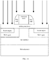
- a conventional processing of manufacturing a self-aligned channel is described below by using FIG. 1 and FIG. 2 .
- a substrate and an epitaxy are used as a semiconductor base, and an arrow direction indicates an implantation direction of an ion (used to form a well region).
- a barrier layer (or referred to as a hard mask) is first used to block implantation of some ions, and the well region is formed below a surface of the semiconductor base other than the barrier layer.
- a dielectric layer continues to be deposited on the hard mask, and then a side wall (Spacer) is formed through dry etching.
- An arrow direction indicates an implantation direction of an ion (used to form a source region and a channel). The ion is implanted into the source region to naturally form a self-aligned channel (Channel).
- the hard mask needs to be deposited on a semiconductor surface to prevent implantation of a high-energy ion, and an ion is implanted on the semiconductor surface to form the well region.
- the dielectric layer needs to be deposited on a semiconductor surface beside the hard mask to form the side wall (spacer), to block implantation of a high-energy ion.
- an ion is implanted on the semiconductor surface, so that the channel is formed below a semiconductor surface covered by the side wall, and the source region is formed below each of a semiconductor surface not covered by the barrier layer and a semiconductor surface not covered by the side wall.
- a thickness of the hard mask depends on implanted ion energy, and larger energy requires a thicker hard mask. It can be learned from the foregoing process that in the process of forming a well region and the process of forming a source region, thicknesses of the barrier layer (that is, the hard mask) are equal to each other. However, depth requirement of the source region is lower than a depth requirement of the well region. It is clearly that a height of the barrier layer used in the process of forming a source region is redundant. In addition, because the height of the barrier layer is large, that is, a step used to form the side wall is large, it is prone to cause poor uniformity of a deposited side wall dielectric. Consequently, the formed side wall is prone to break and collapse. As a result, in the process of forming a channel in the semiconductor device, a width of the formed channel is large, and conduction resistance of the semiconductor device also increases accordingly.
- Conduction resistance of the semiconductor device is an important parameter for measuring quality of the semiconductor device.
- the conduction resistance is directly associated with an area of the semiconductor device, and the conduction resistance is positively correlated with the area of the semiconductor device.
- An increase in the area of the semiconductor device directly causes an increase in manufacturing costs of the semiconductor device.
- how to reduce the conduction resistance of the semiconductor device to improve a yield rate of the semiconductor device and reduce manufacturing costs of the semiconductor device is an unresolved technical problem in a current solution.
- the thickness of the hard mask that blocks ion implantation is relatively large, a process of depositing and etching the side wall is difficult, and the formed side wall is large in size and is not uniform, which results in poor device uniformity, and further increases manufacturing costs. Therefore, how to manufacture a more uniform side wall with a smaller size to form a channel with a smaller width, to reduce the conduction resistance of the semiconductor device and increase a yield rate of the semiconductor device is a technical problem that needs to be urgently resolved currently.
- embodiments of this application provide a semiconductor device manufacturing method and a semiconductor device, to form a self-aligned channel with a smaller size and better uniformity to reduce conduction resistance of the semiconductor device, thereby improving a yield rate of the semiconductor device and reducing manufacturing costs of the semiconductor device.
- FIG. 3 is a semiconductor device manufacturing method according to an embodiment of this application. The method includes the following steps.
- the method shown in FIG. 3 may be applied to a process of manufacturing a semiconductor device, and may be specifically applied to a process of manufacturing a semiconductor device.
- step S1 the semiconductor base is provided.
- the semiconductor base may include an etching stop layer and a substrate located on one side of the etching stop layer, and the other side of the etching stop layer forms a surface of the semiconductor base.
- An ion needs to be implanted in a process of forming a well region, a source region, and a channel in the semiconductor device, and an ion implantation concentration presents a distribution curve in terms of depth of the semiconductor device, so that a surface of the semiconductor device is from small to large, subsequently becomes flat, and then descends.
- the etching stop layer is disposed in the semiconductor base, and the other side of the etching stop layer forms the surface of the semiconductor base, so that in an implantation process after the ion (including a first ion used to form a well region or a second ion used to form a source region) passes through the etching stop layer, damage to the substrate can be reduced by disposing the etching stop layer, and a depth of the implanted ion can be implemented by controlling a thickness of the etching stop layer, thereby further improving a yield rate of the semiconductor device.
- the substrate may indicate a substrate of a semiconductor wafer, which is made of materials such as silicon, silicon carbide, and sapphire.
- a component of the etching stop layer is a silicon compound.
- the silicon compound may include polycrystalline silicon, silicon nitride, silicon oxide, silicon carbide, and the like.
- the composition component of the etching stop layer may be one silicon compound or a mixture of a plurality of silicon compounds. In other words, the etching stop layer may be implemented in a plurality of manners.
- a thickness of the etching stop layer may range from 10 nanometers to 500 nanometers.
- a thickness value of the etching stop layer is limited to 10 nanometers to 500 nanometers, so that on the premise that the etching stop layer has a specific thickness to fulfill the foregoing function, it can be avoided that the etching stop layer is difficult to be removed subsequently due to an excessively large thickness value.
- the etching stop layer is not mandatory.
- the etching stop layer is disposed to ensure that a semiconductor layer is not etched when a hard mask is etched.
- whether the etching stop layer is disposed is not limited herein.
- the semiconductor base further includes an epitaxial layer (or referred to as an epitaxy). As shown in FIG. 4 , the epitaxial layer is located between the etching stop layer and the substrate. Specifically, the semiconductor base may further include the epitaxial layer located between the etching stop layer and the substrate. Implantation of an ion (including a first ion used to form a well region or a second ion used to form a source region) may form a well region, a source region, and a channel on the epitaxial layer, so that the present invention is applicable to a semiconductor structure including a substrate and an epitaxial layer.
- an ion including a first ion used to form a well region or a second ion used to form a source region
- the epitaxial layer has high resistivity relative to the substrate, and the substrate has low resistivity relative to the epitaxial layer.
- the epitaxial layer with high resistivity ensures that the semiconductor device has relatively high breakdown voltage, and the substrate with low resistivity can reduce resistance of the semiconductor device, thereby reducing a saturation voltage drop.
- the epitaxial layer (epitaxial, Epi) may specifically indicate a technology used in a process of manufacturing a semiconductor device to grow a new crystal on an original chip to manufacture a new semiconductor layer.
- the etching stop layer may be deposited on the epitaxial layer in a plurality of manners, for example, based on low-pressure chemical vapor deposition (low-pressure chemical vapor deposition, LPCVD), plasma-enhanced chemical vapor deposition (plasma-enhanced chemical vapor deposition, PECVD), or in another manner. This is not limited herein.
- low-pressure chemical vapor deposition low-pressure chemical vapor deposition, LPCVD
- plasma-enhanced chemical vapor deposition plasma-enhanced chemical vapor deposition
- PECVD plasma-enhanced chemical vapor deposition
- the semiconductor base includes a combination of the etching stop layer, the epitaxy, and the substrate shown in FIG. 4 is used for description. It is clearly that the semiconductor base provided in step S1 may be implemented in another manner other than FIG. 4 .
- the semiconductor base may include only the substrate; or the semiconductor base may include only the substrate and the etching stop layer; or the semiconductor base may include only the substrate and the epitaxial layer; or the semiconductor base is implemented in another manner. This is not limited herein.
- the first hard mask is deposited on the surface of the semiconductor base.
- the first hard mask may be deposited on the surface of the semiconductor base in a plurality of manners, for example, based on low-pressure chemical vapor deposition (low-pressure chemical vapor deposition, LPCVD), plasma-enhanced chemical vapor deposition (plasma-enhanced chemical vapor deposition, PECVD), or in another manner. This is not limited herein.
- low-pressure chemical vapor deposition low-pressure chemical vapor deposition, LPCVD
- plasma-enhanced chemical vapor deposition plasma-enhanced chemical vapor deposition
- PECVD plasma-enhanced chemical vapor deposition
- the second hard mask is deposited on the first hard mask.
- the second hard mask may be deposited on the first hard mask in a plurality of manners, for example, based on low-pressure chemical vapor deposition (low-pressure chemical vapor deposition, LPCVD), plasma-enhanced chemical vapor deposition (plasma-enhanced chemical vapor deposition, PECVD), or in another manner. This is not limited herein.
- low-pressure chemical vapor deposition low-pressure chemical vapor deposition, LPCVD
- plasma-enhanced chemical vapor deposition plasma-enhanced chemical vapor deposition
- PECVD plasma-enhanced chemical vapor deposition
- the first hard mask may include one layer of hard mask, or may include a plurality of layers of hard masks.
- composition components of different layers of hard masks may be the same or different.
- etching dry etching or wet etching
- the second hard mask may also include one layer of hard mask, or may include a plurality of layers of hard masks.
- composition components of different layers of hard masks may be the same or different. In this case, in a process of removing the second hard mask, etching (dry etching or wet etching) may be performed one or more times. This is not limited herein.
- etching dry etching or wet etching
- a component of the second hard mask is different from a component of the first hard mask.
- the first hard mask and the second hard mask that have different components are disposed, so that in the subsequent process of removing the second hard mask, an etching condition that an etching rate at which the component of the second hard mask is etched is relatively large and an etching rate at which the component of the first hard mask is etched is relatively small may be set to reduce damage to the first hard mask in the process of removing the second hard mask.
- an etching selectivity ratio of the second hard mask to the first hard mask is greater than 10 to 1.
- the etching selectivity ratio may indicate a fast/low etching rate of one material relative to another material in a same etching condition.
- damage to the first hard mask can be reduced in the process of removing the second hard mask, because the etching selectivity ratio of the second hard mask to the first hard mask is greater than 10 to 1, that is, in a specific etching condition, an etching rate of the second hard mask is far greater than an etching rate of the first hard mask.
- the etching selectivity ratio of the second hard mask to the first hard mask is greater than 1 to 1.
- the component of the second hard mask is the same as the component of the first hard mask.
- an etching condition for example, an etching liquid concentration or an etching temperature
- an etching condition may be controlled to reduce damage to the first hard mask in the process of removing the second hard mask.
- the component of the second hard mask and the component of the first hard mask both are silicon compounds.
- the silicon compound may include polycrystalline silicon, silicon nitride, silicon oxide, silicon carbide, and the like.
- the composition component of the first hard mask may be one silicon compound or a mixture of a plurality of silicon compounds.
- the composition component of the second hard mask may also be one silicon compound or a mixture of a plurality of silicon compounds. In other words, the first hard mask and the second hard mask may be implemented in a plurality of manners.
- the component of the etching stop layer may be different from that of the first hard mask, or the component of the etching stop layer may be different from that of the second hard mask. Subsequently, an etching condition may be controlled to avoid corrosion of the etching stop layer when the first hard mask (or the second hard mask) is etched.
- an etching selectivity ratio of the first hard mask to the etching stop layer may be greater than 10 to 1.
- a thickness of the first hard mask ranges from 0.1 microns to 3 microns.
- a thickness of the second hard mask ranges from 0.1 microns to 3 microns.
- the first hard mask and the second hard mask are etched through photolithography to form the hard mask pattern.
- a photoresist (or referred to as a photoresist, or referred to as a photoresist, or referred to as a photoresist, and so on) may be coated outside the second hard mask through glue spreading to obtain the hard mask pattern. Then, after the first hard mask and the second hard mask other than the hard mask pattern are etched through dry etching, wet etching, or in another etching manner, the photoresist is removed to obtain the hard mask pattern shown in FIG. 7 .
- the etching stop layer can protect the epitaxial layer.
- the etching stop layer avoids corrosion of the epitaxial layer in the semiconductor device in the process of etching the first hard mask and the second hard mask, and avoids damage to a semiconductor surface in a subsequent ion implantation process.
- an arrow direction indicates an implantation direction of the first ion.
- the first ion that is used to form the well region below the first region is implanted on the surface of the semiconductor base.
- the first region is a region other than the hard mask pattern on the surface of the semiconductor base.
- step S6 to step S10 may be performed in sequence based on an arrow direction shown in FIG. 3 .
- step S5 step S7, step S9, and step S10 may be directly separately performed based on the arrow direction shown in FIG. 3 by skipping (or not performing) step S6 and step S8. This is not limited herein.
- the photoresist is deposited on the surface of the semiconductor base.
- the photoresist covers a surface of the first region.
- Step S6 is an optional execution step.
- the photoresist may further cover an outer surface of the second hard mask.
- a thickness of the photoresist ranges from 0.3 microns to 3 microns.
- the second hard mask is etched through dry etching or wet etching, so that the first hard mask is exposed.
- the photoresist coated in step S6 may protect the first region, so as to avoid corrosion of the semiconductor base in the process of removing the second hard mask in step S7.
- Step S7 the second hard mask may be removed based on execution of step S5 (that is, step S6 is not performed); or the second hard mask may be removed based on execution of step S6. This is not limited herein.
- the photoresist may further cover the second hard mask in an implementation process shown in FIG. 9 .
- the process of removing the second hard mask specifically includes: removing the second hard mask after the photoresist covering the second hard mask is removed.
- the photoresist deposited on the surface of the semiconductor base not only covers the surface of the first region but also covers the surface of the second hard mask.
- the photoresist covering the second hard mask is removed before the second hard mask is removed.
- the photoresist may be indiscriminately deposited in all regions on the surface of the semiconductor base, so that the photoresist covers the surface of the second hard mask and the surface of the first region, and the photoresist unnecessarily needs to be deposited in a specific region, thereby reducing complexity of depositing the photoresist on the surface of the semiconductor base.
- step S7 the second hard mask is removed through wet etching or dry etching, and an etching condition may be restricted, so that medicinal liquid in wet etching or dry etching causes no damage or relatively slight damage to the first hard mask.
- the photoresist is etched through dry etching or wet etching, so that the first region on the surface of the semiconductor base is exposed, that is, a region that is on a surface of the etching stop layer and that is not covered by the first hard mask is exposed.
- step S6 is performed, step S8 is performed; or if step S6 is not performed, step S8 does not need to be performed herein.
- a layer of side wall dielectric may be deposited on the surface of the semiconductor base. Then, the side wall dielectric is etched through dry etching or wet etching to obtain a side wall structure shown in FIG. 14 .
- the side wall dielectric may be deposited on the surface of the semiconductor base in a plurality of manners, for example, based on low-pressure chemical vapor deposition (low-pressure chemical vapor deposition, LPCVD), plasma-enhanced chemical vapor deposition (plasma-enhanced chemical vapor deposition, PECVD), or in another manner. This is not limited herein.
- low-pressure chemical vapor deposition low-pressure chemical vapor deposition, LPCVD
- plasma-enhanced chemical vapor deposition plasma-enhanced chemical vapor deposition
- PECVD plasma-enhanced chemical vapor deposition
- a component of the side wall dielectric may be different from the component of the first hard mask.
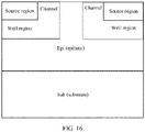
- the second ion is implanted on the surface of the semiconductor base.
- the second ion is used to form a source region below a second region and form a channel (not shown in FIG. 15 ) below a third region.
- the second region is a region that is in the first region and that is not covered by the side wall
- the third region is a region that is in the first region and that is covered by the side wall.
- ion energy of the first ion is greater than ion energy of the second ion.
- Ion energy of the first ion that is implanted on the surface of the semiconductor base and that is used to form the well region is greater than ion energy of the second ion that is implanted on the surface of the semiconductor base and that is used to form the source region and the channel. Because ion energy is positively correlated with an implantation depth, a depth of the well region formed below the surface of the semiconductor base is greater than a depth of the source region formed below the surface of the semiconductor base, thereby meeting depth requirements in different regions in the semiconductor device.
- the method may further include: removing the first hard mask and the side wall. After the source region and the channel are formed below the surface of the semiconductor base, the first hard mask and the side wall that cover the surface of the semiconductor base may be further removed to expose the surface of the semiconductor base.
- step S10 when the channel formed for the semiconductor base in step S10 does not need to be further processed, for example, when the substrate (or the epitaxial layer that may exist) of the semiconductor base is silicon carbide, after the first hard mask and the side wall are removed, gate oxide and a gate dielectric may be further formed on the exposed surface of the semiconductor base, and a gate structure is formed through etching to meet a power-on requirement of the semiconductor device in a specific scenario.
- the first hard mask and the side wall may not need to be removed, and the channel is transferred, through thermal diffusion, to be below the first hard mask or the side wall whose material is polysilicon (polysilicon, poly).
- the first hard mask and the side wall may be directly used as a gate structure of the semiconductor device, so as to meet a pass-through requirement of the semiconductor device in a specific scenario.
- the first hard mask and the side wall need to be removed, as shown in FIG. 16 , based on the well region, the source region, and the channel that are obtained after processing in step S10, the first hard mask and the side wall located on the surface of the semiconductor base are removed through dry etching or wet etching, so that the surface of the semiconductor base is exposed to obtain the semiconductor device.
- the method may further include: removing the etching stop layer.
- the etching stop layer is removed through dry etching or wet etching.
- a barrier layer used to form the well region includes the first hard mask and the second hard mask, and a barrier layer used to form the source region includes only the first hard mask. It is clearly that a thickness of the barrier layer used to form the source region is less than a thickness of the barrier layer used to form the well region. In other words, the thickness of the barrier layer used to form the source region is reduced, so that a side wall with a smaller size can be obtained, so as to form a self-aligned channel with a smaller size and better uniformity to reduce conduction resistance of the semiconductor device, thereby improving a yield rate of the semiconductor device and reducing manufacturing costs of the semiconductor device.
- An embodiment of this application further provides a semiconductor device.
- the semiconductor device may be a semiconductor device manufactured from the semiconductor base shown in FIG. 4 to FIG. 16 , and the semiconductor device may be manufactured by using the method shown in FIG. 3 .
- the semiconductor device includes a channel.
- the chip may include a semiconductor device manufactured from the semiconductor base shown in FIG. 4 to FIG. 16 , and the semiconductor device may be manufactured by using the method shown in FIG. 3 .
Landscapes
- Metal-Oxide And Bipolar Metal-Oxide Semiconductor Integrated Circuits (AREA)
- Drying Of Semiconductors (AREA)
Applications Claiming Priority (1)
| Application Number | Priority Date | Filing Date | Title |
|---|---|---|---|
| CN202110169971.9A CN114883194A (zh) | 2021-02-05 | 2021-02-05 | 一种半导体器件的制造方法和半导体器件 |
Publications (1)
| Publication Number | Publication Date |
|---|---|
| EP4040502A1 true EP4040502A1 (de) | 2022-08-10 |
Family
ID=80218370
Family Applications (1)
| Application Number | Title | Priority Date | Filing Date |
|---|---|---|---|
| EP22155142.7A Withdrawn EP4040502A1 (de) | 2021-02-05 | 2022-02-04 | Verfahren zur herstellung eines halbleiterbauelements sowie halbleiterbauelement |
Country Status (2)
| Country | Link |
|---|---|
| EP (1) | EP4040502A1 (de) |
| CN (1) | CN114883194A (de) |
Citations (4)
| Publication number | Priority date | Publication date | Assignee | Title |
|---|---|---|---|---|
| EP0342952A2 (de) * | 1988-05-17 | 1989-11-23 | Advanced Power Technology Inc. | Abgegrenzter Leistungs-MOSFET mit topographischer Anordnung mit profiljustierender eingelassener Source |
| JP2002299620A (ja) * | 2001-03-30 | 2002-10-11 | Denso Corp | 炭化珪素半導体装置の製造方法 |
| US20100048004A1 (en) * | 2007-01-16 | 2010-02-25 | Koichi Hashimoto | Semiconductor device and process for manufacturing the same |
| CN105161539A (zh) * | 2015-09-10 | 2015-12-16 | 中国科学院微电子研究所 | 碳化硅mosfet器件及其制作方法 |
-
2021
- 2021-02-05 CN CN202110169971.9A patent/CN114883194A/zh active Pending
-
2022
- 2022-02-04 EP EP22155142.7A patent/EP4040502A1/de not_active Withdrawn
Patent Citations (4)
| Publication number | Priority date | Publication date | Assignee | Title |
|---|---|---|---|---|
| EP0342952A2 (de) * | 1988-05-17 | 1989-11-23 | Advanced Power Technology Inc. | Abgegrenzter Leistungs-MOSFET mit topographischer Anordnung mit profiljustierender eingelassener Source |
| JP2002299620A (ja) * | 2001-03-30 | 2002-10-11 | Denso Corp | 炭化珪素半導体装置の製造方法 |
| US20100048004A1 (en) * | 2007-01-16 | 2010-02-25 | Koichi Hashimoto | Semiconductor device and process for manufacturing the same |
| CN105161539A (zh) * | 2015-09-10 | 2015-12-16 | 中国科学院微电子研究所 | 碳化硅mosfet器件及其制作方法 |
Also Published As
| Publication number | Publication date |
|---|---|
| CN114883194A (zh) | 2022-08-09 |
Similar Documents
| Publication | Publication Date | Title |
|---|---|---|
| JP4971559B2 (ja) | 半導体装置の製造方法 | |
| US4258465A (en) | Method for fabrication of offset gate MIS device | |
| US7754572B2 (en) | Semiconductor device and a method of manufacturing thereof | |
| US6710383B2 (en) | MISFET semiconductor device having a high dielectric constant insulating film with tapered end portions | |
| US20130056833A1 (en) | Semiconductor device | |
| US8216908B2 (en) | Extended drain transistor and method of manufacturing the same | |
| US7112497B2 (en) | Multi-layer reducible sidewall process | |
| KR20220074921A (ko) | Ldmos 소자 및 이의 제조방법 | |
| US20230335621A1 (en) | Method for manufacturing trench-type mosfet | |
| CN115377181A (zh) | 半导体装置以及其制作方法 | |
| CN109087943A (zh) | 隧穿场效晶体管结构与其制作方法 | |
| US11456371B2 (en) | Method for making LDMOS device and LDMOS device | |
| CN116314288B (zh) | Ldmos器件的制备方法及其结构 | |
| US12166121B2 (en) | Integrated circuit structure | |
| US20070166902A1 (en) | Method to control the gate sidewall profile by graded material composition | |
| EP4040502A1 (de) | Verfahren zur herstellung eines halbleiterbauelements sowie halbleiterbauelement | |
| CN105308721B (zh) | 在氮化镓器件和集成电路中制备自对准隔离的方法 | |
| JP2022022162A (ja) | 半導体デバイス用デュアルゲート構造 | |
| US20050136595A1 (en) | Method for manufacturing semiconductor device | |
| KR100345365B1 (ko) | 반도체소자의 트랜지스터 형성방법 | |
| TWI241023B (en) | Method for fabricating semiconductor device | |
| US20240021484A1 (en) | Semiconductor structure and preparation method | |
| JPH0369137A (ja) | 半導体集積回路の製造方法 | |
| US10157981B1 (en) | Structure and formation method of semiconductor device structure with well regions | |
| KR100424185B1 (ko) | 트랜지스터 형성 방법 |
Legal Events
| Date | Code | Title | Description |
|---|---|---|---|
| PUAI | Public reference made under article 153(3) epc to a published international application that has entered the european phase |
Free format text: ORIGINAL CODE: 0009012 |
|
| STAA | Information on the status of an ep patent application or granted ep patent |
Free format text: STATUS: REQUEST FOR EXAMINATION WAS MADE |
|
| 17P | Request for examination filed |
Effective date: 20220204 |
|
| AK | Designated contracting states |
Kind code of ref document: A1 Designated state(s): AL AT BE BG CH CY CZ DE DK EE ES FI FR GB GR HR HU IE IS IT LI LT LU LV MC MK MT NL NO PL PT RO RS SE SI SK SM TR |
|
| STAA | Information on the status of an ep patent application or granted ep patent |
Free format text: STATUS: EXAMINATION IS IN PROGRESS |
|
| 17Q | First examination report despatched |
Effective date: 20230201 |
|
| GRAP | Despatch of communication of intention to grant a patent |
Free format text: ORIGINAL CODE: EPIDOSNIGR1 |
|
| STAA | Information on the status of an ep patent application or granted ep patent |
Free format text: STATUS: GRANT OF PATENT IS INTENDED |
|
| INTG | Intention to grant announced |
Effective date: 20230718 |
|
| STAA | Information on the status of an ep patent application or granted ep patent |
Free format text: STATUS: THE APPLICATION IS DEEMED TO BE WITHDRAWN |
|
| 18D | Application deemed to be withdrawn |
Effective date: 20231129 |