EP4042098B1 - Vorrichtung und verfahren zur bildmessung und interferometrie - Google Patents
Vorrichtung und verfahren zur bildmessung und interferometrie Download PDFInfo
- Publication number
- EP4042098B1 EP4042098B1 EP20780605.0A EP20780605A EP4042098B1 EP 4042098 B1 EP4042098 B1 EP 4042098B1 EP 20780605 A EP20780605 A EP 20780605A EP 4042098 B1 EP4042098 B1 EP 4042098B1
- Authority
- EP
- European Patent Office
- Prior art keywords
- measured
- measurement
- light
- configuration
- arm
- Prior art date
- Legal status (The legal status is an assumption and is not a legal conclusion. Google has not performed a legal analysis and makes no representation as to the accuracy of the status listed.)
- Active
Links
Images


Classifications
-
- G—PHYSICS
- G01—MEASURING; TESTING
- G01B—MEASURING LENGTH, THICKNESS OR SIMILAR LINEAR DIMENSIONS; MEASURING ANGLES; MEASURING AREAS; MEASURING IRREGULARITIES OF SURFACES OR CONTOURS
- G01B11/00—Measuring arrangements characterised by the use of optical techniques
- G01B11/30—Measuring arrangements characterised by the use of optical techniques for measuring roughness or irregularity of surfaces
-
- G—PHYSICS
- G01—MEASURING; TESTING
- G01B—MEASURING LENGTH, THICKNESS OR SIMILAR LINEAR DIMENSIONS; MEASURING ANGLES; MEASURING AREAS; MEASURING IRREGULARITIES OF SURFACES OR CONTOURS
- G01B11/00—Measuring arrangements characterised by the use of optical techniques
- G01B11/24—Measuring arrangements characterised by the use of optical techniques for measuring contours or curvatures
- G01B11/2441—Measuring arrangements characterised by the use of optical techniques for measuring contours or curvatures using interferometry
-
- G—PHYSICS
- G01—MEASURING; TESTING
- G01B—MEASURING LENGTH, THICKNESS OR SIMILAR LINEAR DIMENSIONS; MEASURING ANGLES; MEASURING AREAS; MEASURING IRREGULARITIES OF SURFACES OR CONTOURS
- G01B9/00—Measuring instruments characterised by the use of optical techniques
- G01B9/02—Interferometers
- G01B9/02001—Interferometers characterised by controlling or generating intrinsic radiation properties
- G01B9/02007—Two or more frequencies or sources used for interferometric measurement
-
- G—PHYSICS
- G01—MEASURING; TESTING
- G01B—MEASURING LENGTH, THICKNESS OR SIMILAR LINEAR DIMENSIONS; MEASURING ANGLES; MEASURING AREAS; MEASURING IRREGULARITIES OF SURFACES OR CONTOURS
- G01B9/00—Measuring instruments characterised by the use of optical techniques
- G01B9/02—Interferometers
- G01B9/02015—Interferometers characterised by the beam path configuration
- G01B9/02029—Combination with non-interferometric systems, i.e. for measuring the object
- G01B9/0203—With imaging systems
-
- G—PHYSICS
- G01—MEASURING; TESTING
- G01B—MEASURING LENGTH, THICKNESS OR SIMILAR LINEAR DIMENSIONS; MEASURING ANGLES; MEASURING AREAS; MEASURING IRREGULARITIES OF SURFACES OR CONTOURS
- G01B9/00—Measuring instruments characterised by the use of optical techniques
- G01B9/02—Interferometers
- G01B9/02015—Interferometers characterised by the beam path configuration
- G01B9/02032—Interferometers characterised by the beam path configuration generating a spatial carrier frequency, e.g. by creating lateral or angular offset between reference and object beam
-
- G—PHYSICS
- G01—MEASURING; TESTING
- G01B—MEASURING LENGTH, THICKNESS OR SIMILAR LINEAR DIMENSIONS; MEASURING ANGLES; MEASURING AREAS; MEASURING IRREGULARITIES OF SURFACES OR CONTOURS
- G01B9/00—Measuring instruments characterised by the use of optical techniques
- G01B9/02—Interferometers
- G01B9/0209—Low-coherence interferometers
-
- G—PHYSICS
- G01—MEASURING; TESTING
- G01H—MEASUREMENT OF MECHANICAL VIBRATIONS OR ULTRASONIC, SONIC OR INFRASONIC WAVES
- G01H9/00—Measuring mechanical vibrations or ultrasonic, sonic or infrasonic waves by using radiation-sensitive means, e.g. optical means
-
- G—PHYSICS
- G03—PHOTOGRAPHY; CINEMATOGRAPHY; ANALOGOUS TECHNIQUES USING WAVES OTHER THAN OPTICAL WAVES; ELECTROGRAPHY; HOLOGRAPHY
- G03H—HOLOGRAPHIC PROCESSES OR APPARATUS
- G03H1/00—Holographic processes or apparatus using light, infrared or ultraviolet waves for obtaining holograms or for obtaining an image from them; Details peculiar thereto
- G03H1/0005—Adaptation of holography to specific applications
-
- G—PHYSICS
- G03—PHOTOGRAPHY; CINEMATOGRAPHY; ANALOGOUS TECHNIQUES USING WAVES OTHER THAN OPTICAL WAVES; ELECTROGRAPHY; HOLOGRAPHY
- G03H—HOLOGRAPHIC PROCESSES OR APPARATUS
- G03H1/00—Holographic processes or apparatus using light, infrared or ultraviolet waves for obtaining holograms or for obtaining an image from them; Details peculiar thereto
- G03H1/04—Processes or apparatus for producing holograms
- G03H1/0443—Digital holography, i.e. recording holograms with digital recording means
-
- G—PHYSICS
- G01—MEASURING; TESTING
- G01B—MEASURING LENGTH, THICKNESS OR SIMILAR LINEAR DIMENSIONS; MEASURING ANGLES; MEASURING AREAS; MEASURING IRREGULARITIES OF SURFACES OR CONTOURS
- G01B2290/00—Aspects of interferometers not specifically covered by any group under G01B9/02
- G01B2290/70—Using polarization in the interferometer
-
- G—PHYSICS
- G03—PHOTOGRAPHY; CINEMATOGRAPHY; ANALOGOUS TECHNIQUES USING WAVES OTHER THAN OPTICAL WAVES; ELECTROGRAPHY; HOLOGRAPHY
- G03H—HOLOGRAPHIC PROCESSES OR APPARATUS
- G03H1/00—Holographic processes or apparatus using light, infrared or ultraviolet waves for obtaining holograms or for obtaining an image from them; Details peculiar thereto
- G03H1/04—Processes or apparatus for producing holograms
- G03H1/08—Synthesising holograms, i.e. holograms synthesized from objects or objects from holograms
- G03H1/0866—Digital holographic imaging, i.e. synthesizing holobjects from holograms
-
- G—PHYSICS
- G03—PHOTOGRAPHY; CINEMATOGRAPHY; ANALOGOUS TECHNIQUES USING WAVES OTHER THAN OPTICAL WAVES; ELECTROGRAPHY; HOLOGRAPHY
- G03H—HOLOGRAPHIC PROCESSES OR APPARATUS
- G03H1/00—Holographic processes or apparatus using light, infrared or ultraviolet waves for obtaining holograms or for obtaining an image from them; Details peculiar thereto
- G03H1/0005—Adaptation of holography to specific applications
- G03H2001/0033—Adaptation of holography to specific applications in hologrammetry for measuring or analysing
-
- G—PHYSICS
- G03—PHOTOGRAPHY; CINEMATOGRAPHY; ANALOGOUS TECHNIQUES USING WAVES OTHER THAN OPTICAL WAVES; ELECTROGRAPHY; HOLOGRAPHY
- G03H—HOLOGRAPHIC PROCESSES OR APPARATUS
- G03H1/00—Holographic processes or apparatus using light, infrared or ultraviolet waves for obtaining holograms or for obtaining an image from them; Details peculiar thereto
- G03H1/04—Processes or apparatus for producing holograms
- G03H1/0443—Digital holography, i.e. recording holograms with digital recording means
- G03H2001/0445—Off-axis recording arrangement
-
- G—PHYSICS
- G03—PHOTOGRAPHY; CINEMATOGRAPHY; ANALOGOUS TECHNIQUES USING WAVES OTHER THAN OPTICAL WAVES; ELECTROGRAPHY; HOLOGRAPHY
- G03H—HOLOGRAPHIC PROCESSES OR APPARATUS
- G03H1/00—Holographic processes or apparatus using light, infrared or ultraviolet waves for obtaining holograms or for obtaining an image from them; Details peculiar thereto
- G03H1/04—Processes or apparatus for producing holograms
- G03H1/0443—Digital holography, i.e. recording holograms with digital recording means
- G03H2001/0452—Digital holography, i.e. recording holograms with digital recording means arranged to record an image of the object
-
- G—PHYSICS
- G03—PHOTOGRAPHY; CINEMATOGRAPHY; ANALOGOUS TECHNIQUES USING WAVES OTHER THAN OPTICAL WAVES; ELECTROGRAPHY; HOLOGRAPHY
- G03H—HOLOGRAPHIC PROCESSES OR APPARATUS
- G03H2222/00—Light sources or light beam properties
- G03H2222/40—Particular irradiation beam not otherwise provided for
- G03H2222/45—Interference beam at recording stage, i.e. following combination of object and reference beams
Definitions
- the present invention relates to a device for performing combined full-field imaging and interferometry measurements of an object. It also relates to a method for combined imaging and interferometry measurements.
- the field of the invention is, in a non-limiting manner, that of full-field interferometric optical systems for measuring the shapes and surfaces of objects.
- This type of sensor uses a measuring optical beam that interacts with the object and a reference optical beam that are recombined on a sensor such as a camera to produce interference signals. They are called “full field” when the object is imaged on the camera according to a field of view.
- the processing of the interference signals makes it possible to reconstruct a phase profile or a shape of the object according to the field of view.
- the images obtained on the camera under these conditions are a mixture of the image of the object and interference fringes.
- An aim of the present invention is to overcome the drawbacks of the devices and methods of the prior art.
- Another aim of the invention is to propose a device and a method allowing the acquisition of images and interferometric signals on an object, under optimal conditions, both for imaging and for interferometric signals.
- the measuring device is configured, according to a first configuration, called interferometry, to illuminate the reference arm and the measuring arm with the at least one light source and to direct the light coming from the arm.
- measuring arm and the reference arm to a first optical sensor among the optical sensors so as to form an interference signal.
- the measuring device is configured, according to a second configuration, called imaging, to illuminate at least the measuring arm and to direct the light coming from the measuring arm only towards an optical sensor among the optical sensors so as to form an image of the surface of the object.
- the device further comprises means for determining a position of the surface to be measured relative to a conjugate object plane of the first optical sensor from a measurement of said surface according to the imaging configuration, and digital processing means configured to use said position of the surface to be measured to correct effects of light propagation between the conjugate plane of the first optical sensor and said surface to produce, from the interference signal, information on the surface of the object.
- an "object” may designate any type of object, in particular mechanical, electronic or optical. It may thus for example designate, in a non-limiting manner, a lens, a blade or an assembly of lenses and/or other optical components such as an objective, a microelectronic element or circuit, a MEMS microsystem (in English, micro-electromechanical system ) or MOEMS (in English, micro-opto-electromechanical system ).
- the measurements make it possible to determine, for example, shapes, topologies or movements, such as vibrations, of a surface of the object.
- the surface to be measured may be an external surface of the object, or a "buried" surface, located between other surfaces of the object. This surface may also be an interface between two layers or two structures of the object.
- the measurements are performed by a device that can operate in an interferometry configuration and in an imaging configuration.
- an interference signal is detected between a measurement beam coming from the surface to be measured and a reference beam.
- This interference signal in full field, is obtained when the measurement and reference arms of the interferometric device are illuminated by the same light source and configured so that the difference in optical paths of the respective beams incident on the optical sensor is less to the coherence length of the source.
- an image of the object surface is acquired by capturing the measurement beam from the surface.
- Interference and imaging measurements are performed over a specified field of view. by the measuring means of the device. The measurements are carried out in open field.
- the conditions for illumination of the object and acquisition of images and interference signals are similar.
- the object is illuminated in the same way by the light from the measuring arm and through the same focusing optics, in bright field.
- the measuring beam coming from the surface of the object is acquired through this same focusing optics.
- This arrangement of the device allows an optimal correspondence between the interference signals and the images. This correspondence allows their combined use to achieve a more complete characterization of the object.
- the images provided by imaging and the interference signals provided by interferometry are complementary.
- interference signals provide a measure of the shape or height of the surface considered.
- the images provide more precise and more complete information in the plane of the object surface, monochrome or color, compared to interferometry. Even if the interference signals also make it possible to obtain intensity information, this information is strongly degraded by the presence of artifacts related to interference fringes and phase unfolding conditions, in particular around height transitions of the measured surface of the object.
- the images can be exploited by implementing image analysis techniques to, for example, segment areas, identify materials or elements of the image, or precisely measure lateral dimensions.
- the achievable lateral resolution can be very different depending on the type of interferometry implemented, and in particular when using an off-axis interferometry configuration with measurement and reference beams incident on the sensor at a non-zero angle. Even if this configuration allows efficient detection in the Fourier domain, it has the disadvantage that, since the information is encoded as a modulation of an interference fringe network in the interference image, the lateral resolution depends on the periodicity of these fringes, and is therefore significantly lower than the resolution of the sensor used.
- the measuring device further comprises means for switching between the imaging configuration and the interferometry configuration.
- the tilting means may comprise a blocking element for blocking or preventing the transmission of light into the reference arm of the interferometric device.
- This blocking element may be for example a mechanical or electro-optical shutter, or a means for modifying for example an alignment of an element such as a mirror of the reference arm.
- the measuring device may comprise a first light source arranged to illuminate the measuring arm and the reference arm of the interferometric device.
- the measuring device according to the invention can comprise two light sources.
- it may comprise a second light source arranged to illuminate only the measuring arm of the interferometric device.
- the first light source can be used when the device is in the interferometry configuration
- the second light source can be used when the device is in the imaging configuration
- the spectral and/or polarization properties of the light emitted respectively by the first and second light sources may be different, or vary from one light source to another.
- the first light source and the second light source can be used simultaneously.
- the two light sources can also be used sequentially.
- the measuring device according to the invention can comprise two optical sensors.
- the first optical sensor may be configured to detect light from the first light source (in the interferometry configuration), and the second optical sensor may be configured to detect light from the second light source (in the imaging configuration).
- the first and second optical sensors can comprise, or be positioned downstream of, spectral filters or polarizing elements adapted to separate the light coming from the first and second light sources respectively.
- the at least one optical sensor may comprise a monochrome or color matrix sensor (e.g. CMOS or CCD type).
- a color sensor can be used to simultaneously acquire light from a first light source in the interferometry configuration, and from a second light source in the imaging configuration.
- two light sources with distinct spectral contents are used, and a color sensor with, for example, spectral filters positioned on the pixels so as to selectively detect the light from the first source on certain pixels and the light from the second source on other pixels.
- the interference signal and the image can thus be separated at the sensor output.
- the measuring device may further comprise positioning means configured to relatively position a conjugate object plane of the at least one optical sensor at the surface to be measured of the object.
- the focusing distance of the light in the measuring arm, and/or the position of the surface to be measured in order to position the surface of the object in the conjugate object plane of the optical sensor(s).
- This makes it possible in particular to optimize the imaging conditions of the surface of the object, and/or the optical power recoupled into the sensor.
- the positioning of the object to be measured in the conjugate object plane of the sensor allows easier reconstruction of the surface to be measure from the interference signal, in particular avoiding optical aberrations due to the defocusing effect.
- the interferometric device may comprise a full-field interferometer, configured to detect a full-field interference signal in a field of view.
- the surface to be measured can be imaged according to the field of view in a single measurement.
- the interferometric device may comprise a Michelson interferometer, with measuring and reference arms operating in reflection.
- the interferometric device may comprise a Mach-Zehnder interferometer, with measuring and reference arms operating globally in transmission.
- the method according to the invention allows the acquisition and processing of images and interference signals. In particular, it allows a combined use of the images and interference signals obtained to deduce information on the object. It is thus possible to combine information from imaging and interferometry measurements to produce more complete information on the object.
- the surface measurements according to the interferometry and imaging configurations can be carried out simultaneously. This can be achieved in particular by implementing two light sources and two optical sensors, or a color optical sensor, as described above.
- the parallel acquisition of interference signals and images is particularly well suited to carrying out dynamic measurements on a moving object.
- shape measurements produce an erroneous result because they integrate the effects of propagation of the light wave between the conjugate object plane of the detector and the surface to be measured. For example, these propagation effects can appear, for surface shape measurements, in the form of estimation errors of the overall shape or of the real curvatures of these shapes.
- the electromagnetic field is digitally propagated over a known distance to the position of the conjugate image plane of the measured surface to obtain surface profile information. Thanks to the images acquired in the imaging configuration, the position of this conjugate image plane of the surface (or of the conjugate object plane of the detector) is known precisely, even in the presence of diffractive structures.
- the processing of the interference signal can be carried out by an analysis by profilometry of a plurality of interferograms acquired for the same surface to be measured.
- Profilometry is based on the processing of sequences of interferograms acquired for a plurality of optical path differences in the interferometric device, and which constitute the interference signal. These sequences can be acquired in different ways depending on the analysis technique implemented.
- the plurality of interferograms may in particular be acquired using a phase shift interferometric method or a vertical scanning interferometric method.
- the processing of the interference signal can implement a calculation method by digital holography.
- An interference signal or interferogram is recorded. Then a digital holography method is used to reconstruct the considered surface digitally, by simulating the process of illumination of the interferogram on the detector with a digital reference wave.
- a digital holography method is used to reconstruct the considered surface digitally, by simulating the process of illumination of the interferogram on the detector with a digital reference wave.
- the method according to the invention can comprise a step of obtaining information on the surface to be measured combining intensity information in gray levels and/or in color obtained in imaging configuration and shape and/or profile information obtained in interferometry configuration.
- the method according to the invention can be implemented to measure the shapes and/or positions of surfaces or interfaces of an object as described above. It is also particularly suitable for vibrometry measurements in order to know the vibrations of an object such as a MEMS in the field of view: The vibrations in the plane of the object can be deduced from the images, and out-of-plane vibrations can be inferred from the interference signals.
- the method according to the invention can thus comprise a step of obtaining information on displacement or vibration of the surface to be measured, comprising obtaining information on displacement or vibration in the plane of this surface from images in imaging configuration, and obtaining information on displacement or vibration outside the plane of this surface from interference signals in interferometry configuration.
- the measuring device is arranged to carry out measurements of a surface to be measured of an object, such as an optical element.
- the device comprises at least one light source, at least one optical sensor or detector and an interferometric device having a measuring arm and a reference arm.
- the at least one source is preferably a low coherence source, the light of which is directed towards the surface to be measured through a focusing optic, such as an objective. The light coming from the surface to be measured is directed towards the at least one optical sensor.
- the measuring device can be configured in an interferometry configuration and an imaging configuration.
- the reference arm and the measuring arm of the interferometer are illuminated, and light from the measuring arm and the reference arm is directed toward the at least one detector to produce there an interference signal between the measuring beam reflected by the surface to be measured and the reference beam coming from the reference arm.
- At least the measuring arm of the interferometer is illuminated, and light from the measuring arm only is directed to the at least one optical sensor to produce an image of the surface to be measured there.
- the measuring device further comprises digital processing means. These processing means are configured to produce, from the measured interference signal and the image, information on the surface to be measured according to a field of view. These processing means comprise at least one computer, a central or calculation unit, a microprocessor, and/or suitable software means.
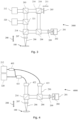
- FIG. 1 is a schematic representation of a measuring device according to a first embodiment of the invention.
- the measuring device 1000 comprises a full-field low-coherence interferometric device of the Michelson or Linnik type.
- the interferometer is formed by a splitter element 104, for example in the form of a cube or a splitter plate, with a measuring arm which directs a measuring beam 106 towards a surface to be measured of an object 100, and a reference arm with a mirror 105 for forming a reference beam 116.
- the interferometer is illuminated by a light source 112 via a lighting splitter element 103, for example in the form of a cube or a splitter plate.
- the source 112 may be low coherence, with a coherence length of the order of a few microns or a few tens of microns for example, or more coherent, with a coherence length of a few hundred microns or more. It may in particular comprise, for example, a superluminescent diode (SLD), a laser diode, a thermal light source (halogen lamp, etc.) or a supercontinuum source.
- SLD superluminescent diode
- laser diode a laser diode
- thermal light source halogen lamp, etc.
- It may also include a filtering device, for example with a grating and a slit, or interference filters, to adjust the coherence length as required. It may be arranged to emit in visible or near infrared wavelengths, around one or more wavelengths.
- the separating elements 103, 104 can be non-polarizing, or polarizing and associated with quarter-wave plates to make lossless couplers.
- the measurement beams 106 and reference beams 116, respectively reflected in the two arms of the interferometer, are directed via the lighting splitter plate 103 towards a camera 101 with a sensor or detector 102 comprising a detection matrix, for example of the CMOS or CCD type.
- the device 1000 also comprises a focusing lens or objective 107, and a tube lens 109, arranged to define a conjugate object plane of an image plane formed on the detector 102.
- the reference arm further comprises an objective 110 which also defines, with the tube lens 109, a conjugate reference object plane of the image plane of the detector 102.
- the device 1000 is a full-field imaging device, which makes it possible to image surfaces or interfaces of the object to be measured 100 on the detector 102.
- the device 1000 includes optical elements for focusing the illumination beam into the rear focal plane of the focusing lens 107 and the reference arm lens 110.
- the illumination beams are not shown in the figure for clarity.
- the device 1000 also comprises a displacement means 108 whose function is to move the object plane conjugate to the image plane formed by the detector 102, so as for example to image the surfaces or interfaces of the object on the detector 102.
- This displacement means 108 can comprise a system for moving the focusing objective 107 or lenses of this objective, for example with a linear or helical translation device.
- this moving means 108 may comprise a translation device or plate for moving the device 1000 relative to the object to be measured 100, or vice versa.
- the device 1000 may also optionally comprise a displacement means 111 for varying the length of the reference arm, for example in the form of a translation plate 111 moving the reference mirror 105.
- the objective 110 of the reference arm may also be adjustable to maintain the reference mirror 105 in an object plane conjugate to the image plane formed by the detector 102.
- This displacement means 111 makes it possible to adjust the relative difference in optical paths between the measuring arm and the reference arm of the interferometer, so as to adjust the area of appearance of the interference fringes.
- the device 1000 also comprises a shutter 113 for interrupting the beam of the reference arm, so that this beam does not reach the detector 102.
- This shutter can be of any type, such as for example a mechanical shutter (diaphragm), or electronic (for example based on liquid crystals). It can also be produced with an element moving the reference mirror 105, for example so as to misalign it.
- FIG. 2 is a schematic representation of a measuring device according to a second embodiment of the invention.
- the measuring device 2000 comprises a full-field low-coherence interferometric device of the Mach-Zehnder type.
- the interferometer comprises a measuring arm which directs a measuring beam 206 towards the surface to be measured of an object 100, and a reference arm in which a reference beam 216 propagates.
- the interferometer is illuminated by a light source 212 via a lighting splitter element 203, for example in the form of a cube or a splitter plate.
- the source 212 may be low coherence, with a coherence length of the order of a few microns or a few tens of microns for example, or more coherent, with a coherence length of a few hundred microns or more. It may in particular comprise for example a superluminescent diode (SLD), a laser diode, a light source thermal (halogen lamp, etc.) or a supercontinuum source.
- SLD superluminescent diode
- laser diode a laser diode
- halogen lamp halogen lamp
- It may also include a filtering device, for example with a grating and a slit, or interference filters, to adjust the coherence length as required. It may be arranged to emit in visible or near infrared wavelengths, around one or more wavelengths.
- the light from the source 212 is separated into a measuring beam 206 and a reference beam 216 by a first splitter element 203, for example in the form of a cube or a splitter blade.
- the interferometer comprises a second splitter element 214 in the measuring arm, for example in the form of a cube or a splitter blade, for directing the measuring beam 206 towards the object to be measured 100, and transmitting the light reflected in this object.
- a second splitter element 214 in the measuring arm for example in the form of a cube or a splitter blade, for directing the measuring beam 206 towards the object to be measured 100, and transmitting the light reflected in this object.
- the device also comprises, in the reference arm, an adjustment element for directing and varying the length of the optical path of the reference arm.
- This element can be produced for example with a splitter element in the form of a cube or a splitter blade 210, and a reference mirror 205 movable in translation by translation means 211 such as a translation plate.
- the measurement beams 206 and reference beams 216 are then combined by means of a splitter element 204, for example in the form of a cube or a splitter blade, and directed towards a camera 201 with a sensor or detector 202 comprising a detection matrix, for example of the CMOS or CCD type.
- a splitter element 204 for example in the form of a cube or a splitter blade
- a sensor or detector 202 comprising a detection matrix, for example of the CMOS or CCD type.
- the Mach-Zehnder interferometer can be made with non-polarizing elements, or polarizing ones and associated with quarter-wave or half-wave plates to make lossless couplers. It can also be made, at least partially, with optical fibers.
- the device also comprises a focusing lens or objective 207, and a tube lens 209, arranged so as to define an object plane conjugate to an image plane formed on the detector 202.
- the device 2000 is also a full-field imaging device, which makes it possible to image surfaces or interfaces of the object to be measured 100 on the detector 202.
- the device 2000 includes optical elements for focusing the illumination beam into the rear focal plane of the focusing lens 207.
- the illumination beams are not shown in the figure for clarity.
- the device 2000 also comprises a displacement means 208 whose function is to move the object plane conjugate to the image plane formed by the detector 202, so as for example to image the surfaces or interfaces of the object 100 on the detector 202.
- This displacement means 208 may comprise a system for moving the focusing objective 207 or lenses of this objective, for example with a linear or helical translation device.
- this displacement means 208 may comprise a translation device or plate for moving the device 2000 relative to the optical element 100, or vice versa.
- the device 2000 also comprises a shutter 213 for interrupting the beam from the reference arm, so that this beam does not reach the detector 202.
- This shutter can be of any type, such as for example a mechanical shutter (diaphragm) or electronic (based on liquid crystals, etc.).
- FIG. 3 is a schematic representation of a measuring device according to a third embodiment of the invention.
- the 3000 measurement device comprises a full-field low-coherence interferometric device of the Mach-Zehnder type.
- the 3000 device differs from the 2000 device shown in the Figure 2 in that it comprises a second light source 320 inserted into the measuring arm via a splitter element 321 in the form of a cube or a splitter blade.
- This second light source 320 may be identical to the first source 212, or different. It may in particular be broad spectrum, in a spectral band similar to or comprising the spectrum of the first source 212, or different from the spectrum of the first source 212.
- the beam from this second light source 320 is also focused in the rear focal plane of the focusing lens 207 (as for the first source 212), in order to illuminate the object 100 through this focusing objective 207 with a uniform illumination beam.
- the second source 320 does not generate a reference beam 216.
- the device 3000 also differs from the device 2000 in that it does not include a shutter 213 making it possible to interrupt the beam from the reference arm.
- the first source 212 and the second source 320 can be used alternately.
- the device allows the acquisition of interferometric measurements, in the interferometry configuration.
- the device allows the acquisition of imaging measurements, in the imaging configuration.
- the first source 212 and the second source 320 can be used simultaneously, with a color detector 202.
- a color detector 202 with for example spectral filters positioned on the pixels so as to selectively detect on certain pixels the light from the first source 212 and on other pixels the light from the second source 320. It is thus possible to separate the interference signals and the image at the detector output.
- interferometry measurements and the imaging measurements are acquired under the same illumination conditions of the object 100 and through the same imaging system, for optimal correspondence.
- FIG. 4 is a schematic representation of a measuring device according to a fourth embodiment of the invention.
- the 4000 measurement device comprises a full-field low-coherence interferometric device of the Mach-Zehnder type.
- the device 4000 differs from the device 3000 shown in the Figure 3 in that the first source 212 and the second source 320 are fibered.
- the first source is connected to a first fiber coupler 403 which plays the role of the splitter element 203 of the device 3000, to generate by through two optical fibers and two collimators 422 and 423, respectively, the measuring beam 206 and the reference beam 216.
- the second source is inserted into the measuring arm via a second fiber coupler 421, which plays the role of the splitter element 321 of the device 3000.
- the first source 212 and the second source 320 can be used alternately, or simultaneously with a color detector 202.
- the second source can be inserted into the measuring arm by means of a freely propagating splitter element 321, for example in the form of a cube or a splitter blade, positioned between the collimator 422 and the splitter element 214.
- FIG. 5 is a schematic representation of a measuring device according to a fifth embodiment of the invention.
- the 5000 measurement device includes a Michelson type full-field low coherence interferometric device.
- Device 5000 differs from device 1000 shown in the Figure 1 in that it comprises a second light source 520 inserted into the measuring arm via a splitter element 521, for example in the form of a cube or a splitter blade.
- This splitter element 521 is inserted between the splitter element 104 of the Michelson interferometer and the focusing optics 107.
- the device 5000 may not comprise a shutter 113.
- the first source 212 and the second source 520 can be used alternately, or simultaneously with a color detector 102.
- FIG. 6 is a schematic representation of a measuring device according to a sixth embodiment of the invention.
- the 6000 measurement device includes a full-field low-coherence interferometric device of the Mach-Zehnder type.
- the 6000 device differs from the 3000 device shown in the Figure 3 in that it comprises a second camera 625 with a detector 624 comprising a detection matrix, for example of the CMOS or CCD type.
- the device 6000 also comprises a tube lens 623, arranged so as to define with the focusing lens 207 an object plane conjugate to an image plane formed on the detector 624 of the second camera 625.
- the first and second cameras and their respective tube lenses may be arranged to define conjugate image planes of a same object plane, at the object 100. Furthermore, the first and second cameras and their tube lenses may be identical to achieve optimal image matching.
- the first and second cameras and their respective tube lenses may be arranged to define conjugate image planes of distinct object planes at the object 100.
- These object planes may for example be shifted by a known amount, to allow for example the acquisition of interferometric signals from a surface to be measured outside a conjugate image plane of this surface.
- the first and second cameras are separated by a splitter element 622.
- the splitter element and the light sources are preferably arranged such that the light from each source reaches only one camera.
- the light from the first source 212 for the interferometric mode reaches only the first camera 201
- the light from the second source 320 for the imaging mode reaches only the second camera 625.
- light sources with distinct spectra and a dichroic splitter element 622 can be used.
- Light sources with different polarizations and a polarizing splitter element 622 or one capable of separating polarizations can also be used.
- the first source 212 and the second source 320 can be used simultaneously, for simultaneous acquisition of images and interferometric signals.
- the splitter element can be arranged so that light from each source reaches both cameras.
- the two cameras can be different, for example color and monochrome, to acquire different information.
- the devices 4000 or 5000 may also comprise a second camera 625 and an element separator 622, arranged with the first camera in the same manner as for the device 6000.
- the two cameras and the two light sources can be arranged in the same way and also used in the same way as described for the 6000 device.
- the devices 1000 or 2000 may also comprise a second camera 625 and a separator element 622, arranged with the first camera in the same manner as for the device 6000.
- the measuring device can be used to implement the steps of a measuring method according to the invention which will be described subsequently.
- FIG. 7 is a schematic representation of a non-limiting exemplary embodiment of a measuring method according to the invention.
- Process 10 shown in the Figure 7 , comprises a step 12 of measuring the surface to be measured by means of the measuring beam 106, 206, in the interferometry configuration.
- Each of the measuring devices 1000, 2000, 3000, 4000, 5000, 6000 described above can be used to perform the surface measurement in the interferometry configuration.
- the measuring and reference arms of the full-field interferometric device are illuminated by the same (first) light source 112, 212, and balanced so that the difference in optical paths of the reference and measuring beams incident on the (first) camera 101, 201 is less than the coherence length of the source, a full-field interference signal is obtained on the detector 102, 202.
- the method 10 also comprises a step 14 of measuring the surface to be measured by means of the measuring beam 106, 206, in the imaging configuration.
- Imaging measurement step 14 may be performed sequentially or in parallel with interferometry measurement step 12.
- the imaging and interferometry measurements are performed sequentially, with the shutter 113, 213 open for the interferometry measurements and closed for the imaging measurements;
- the imaging and interferometry measurements can be performed sequentially, with the light sources turned on alternately. Only the first source 112, 212 is turned on for the interferometry measurements, while only the second source 320, 520 is turned on for the imaging measurements.
- the light sources can be switched on simultaneously, and imaging and interferometry measurements performed simultaneously.
- the imaging and interferometry measurements are performed sequentially or simultaneously.
- the two light sources 212, 320 can be switched on alternately or simultaneously.
- the illumination of the surface to be measured 100 is carried out in the same manner as in the interferometry configuration, through the focusing lens 207. Furthermore, with the exception of the embodiment of the device 6000 shown in the Figure 6 , the acquisition of the image of the object and the interference signal is carried out through the same imaging system and on the same camera. This allows for an optimal match between the images and the interference signals. In the case of the 6000 device, the same result can be obtained by adjusting and calibrating the cameras.
- the optical shapes of these must be determined beforehand, and corrected for propagation effects as described below.
- the interference signal and the image obtained for a surface to be measured are digitally processed, in order to deduce information on this surface.
- the interference signal is processed during an interferometric processing step 17, and the image is processed during an imaging processing step 18.
- the processing steps 17, 18 can be carried out sequentially or in parallel.
- optical shape information of the measured surface is determined. This optical shape is called “apparent” because it is affected by any interfaces and media crossed. It is deduced from the interferometric measurements.
- profilometric methods can be used to perform step 17a.
- the profilometry is based on the processing of interferogram sequences.
- the measurement and reference beams are preferably adjusted so as to be incident on the detector with propagation directions that are essentially parallel or coincident, or slightly inclined, so as to produce flat or weakly modulated hue interferograms.
- a first example of such a profilometric method implements algorithms based on phase stepping interferometry (PSI).
- PSI phase stepping interferometry
- a plurality of interferograms (constituting the interference signal) is acquired for a plurality of values of optical path or phase difference between the measurement and reference beams, within the limit of the coherence length of the light source.
- the phase and possibly the amplitude at any point of the field of view 108 of the interference signal thus constituted are determined by applying a known algorithm, such as for example the Carré algorithm, to the succession of interferograms obtained at the point considered for the different phase shifts, and by unfolding the phase thus obtained modulo 2 pi.
- a known algorithm such as for example the Carré algorithm
- a second example of a profilometric method implements algorithms based on vertical scan interferometry (VSI).
- VSI vertical scan interferometry
- a low coherence or broad spectrum light source is used.
- a plurality of interference signals are acquired for a plurality of optical delays between the measurement and reference arms of the interferometer, in a range of optical delays preferably extending beyond the coherence length of the light source.
- the optical delay for which the optical path difference between the measurement beam reflected on the surface or interface and the reference beam is zero is detected. For this, one can detect, for example, the maximum amplitude of the interferogram envelope or the position where the phase of the interferogram is zero. One thus directly obtains the optical shape L m ( r d ) of the surface.
- a digital holography method may be used.
- the measurement and reference beams are adjusted, preferably, so that they are incident on the detector with propagation directions inclined, or forming an angle between them.
- a coherent light source or at least one whose coherence length is sufficiently large compared to the differences in optical paths considered, is used.
- an interference signal, or interferogram, I m ( rd ) is obtained on the detector in which the phase information is encoded in a network of fringes in the direction of inclination of the beams.
- the first two terms correspond to the zero order, the third and fourth terms to the real and virtual images respectively.
- E R ⁇ E m r d FFT ⁇ 1 FFT I m r d M , where FFT is the fast Fourier transform and FFT -1 is its inverse.
- M is the filter applied in the frequency domain to filter the term corresponding to the real image so as to preserve the spatial frequencies present in the numerical aperture of the focusing lens.
- E m r d E RD E R ⁇ E m r d .
- this step can also be performed in the Fourier domain by translating the baseband filtered image (around the zero frequency).
- optical or geometric shape obtained as described above is a shape as projected onto the detector.
- the effect of the optical system between the surface and the detector must also be taken into account, in a step 17b of the method 10.
- the aberrations of the optical system can be done for example by calibration, by carrying out measurements on a mirror positioned in place of the object to be measured 100. It is thus possible to determine an optical shape resulting from these aberrations, which can be subtracted from the measured optical shape. It is thus also possible to take into account the phase profile of the reference beam on the detector. This makes it possible to improve the accuracy of the shape measurement carried out by the method according to the invention.
- the electromagnetic field E m ( rd ) in the image plane can be determined by numerically propagating the electromagnetic field measured at the detector to this plane.
- Profilometry algorithms such as PSI or digital holography have unambiguous measurement ranges limited to the wavelength. This measurement range can of course be extended according to well-known techniques by performing measurements at several wavelengths.
- the images can be processed according to known techniques. They have the advantage of not being affected by interference signals and make it possible to exploit the resolution of the camera as best as possible. It is then possible to implement image analysis techniques to, for example, segment areas according to predefined criteria, identify materials or elements of the image, or precisely measure lateral dimensions.
- results of the interferometric and imaging treatments obtained during processing phase 16 represent complementary information on the surface considered. Their combined use allows a more complete characterization of the object surface.
- the interferometry signals provide a measurement of the shape or height of the surface.
- interferometry signals also allow obtaining intensity information.
- this information is strongly degraded by the presence of artifacts related to interference fringes and phase unfolding conditions, particularly around surface height transitions.
- the achievable lateral resolution can be very different depending on the type of interferometry implemented, and in particular when using an off-axis interferometry configuration with measurement and reference beams incident on the detector with a non-zero angle.
- This configuration is notably used in digital holography because it allows efficient detection in the Fourier domain.
- the lateral resolution depends on the periodicity of these fringes, and is therefore significantly lower than the resolution of the camera used.
- the device and the method according to the invention allow combined exploitation of interferometry and imaging measurements.
- the method 10 comprises a step 19 of obtaining information on the surface to be measured.
- a step 19 of obtaining information on the surface to be measured To carry out this step 19, an intensity information in gray levels and/or in color obtained in imaging configuration and a shape and/or profile information obtained in interferometry configuration are combined.
- the combined exploitation of the interferometric signals and images obtained can be used in various fields.
- the device and the method according to the invention can be implemented in the field of vibrometry.
- the measuring method according to the invention makes it possible to carry out vibration measurements of an object such as a MEMS or a MEMS element, such as a membrane or an electrostatic comb-shaped actuator.
- the aim is to measure vibrations in the field of view, in the plane (X, Y) and out of the plane (Z).
- the device 6000 with two cameras which allow simultaneous acquisitions is implemented.
- the interferometric signals are acquired in an off-axis interferometry configuration, and processed using digital holography techniques as described above. This allows to obtain a complete measurement of the object surface shape, for each acquisition and at high frame rate.
- the temporal sequence of these shapes or profiles allows to describe the displacements or vibrations of the surface at least out of the plane (Z). To measure high frequency vibrations, it is possible to use pulsed or stroboscopic illumination.
- a parallel acquisition of images with the second camera and the second source is carried out synchronously (for illumination and acquisition) with the acquisition of the interferometric signals.
- the acquisitions in the two configurations are synchronous, the complete vibration or displacement of the MEMS can be described or tracked efficiently in the field of view, in the (X, Y) plane and out of the (Z) plane.
- the device and method according to the invention are implemented for the determination of a conjugate object plane.
- the surface must be positioned in or near a conjugate plane of the detector, in the imaging sense, so that there is sufficient light reflected from the surface and thus power coupled back into the imaging system to enable a measurement.
- the optical path difference between the surface-reflected measurement beam and the reference beam must be less than the coherence length of the light source to allow interference fringes to appear on the detector.
- these two conditions may not be satisfied at the same location or in the same plane, depending on the balancing of the interferometer. This is particularly the case when the measuring beam passes through layers of material or refractive surfaces (lenses) before reaching the surface to be measured. It may then be necessary to adjust separately the position of the conjugate object plane and the optical path difference between the measuring and reference beams. This also has the consequence that in the general case it is not possible to use interference fringes to determine a conjugate object plane, although they strongly impact the quality of the interferometric image.
- the shape measurements produce an erroneous result because they integrate the effects of wave propagation between the conjugate object plane of the detector and the surface. It is therefore necessary to locate this conjugate plane precisely in order to either position the surface of the object precisely in this plane or to propagate by calculation the electromagnetic field detected on the detector in the interferometric configuration in the conjugate image plane of the surface to be measured of the object.
- the measuring device according to the invention is used in the imaging configuration, in order to obtain an image of the surface not disturbed by interference fringes, to determine the position of the surface to be measured relative to the detector conjugate object plane.
- This position can be determined by analyzing images acquired during a scan, for example by determining the image in which the high spatial frequencies are maximized.
- the conjugate object plane of the detector is placed at a known distance from the position for which the conjugate object plane of the detector is positioned at the surface to be measured.
- the visibility of the interference fringes can optionally be optimized by varying the optical path difference between the measurement and reference beams.
- the interference signals are acquired and processed to deduce an electromagnetic field or wavefront expression at the detector.
- this electromagnetic field is digitally propagated to the position of the conjugate image plane of the measured surface, using a known model as described above, to obtain the surface profile information.
Landscapes
- Physics & Mathematics (AREA)
- General Physics & Mathematics (AREA)
- Engineering & Computer Science (AREA)
- Computing Systems (AREA)
- Theoretical Computer Science (AREA)
- Instruments For Measurement Of Length By Optical Means (AREA)
- Length Measuring Devices By Optical Means (AREA)
Claims (17)
- Vorrichtung (1000, 2000, 3000, 4000, 5000, 6000) zum Messen einer Oberfläche eines Objekts (100), wobei die Vorrichtung umfasst:- mindestens eine Lichtquelle (112, 212, 320, 520);- einen optischen Sensor oder eine Vielzahl von optischen Sensoren (102, 202, 624); und- eine interferometrische Vorrichtung, die einen Messarm und einen Referenzarm aufweist, wobei der Messarm konfiguriert ist, um das Licht, das von der mindestens einen Lichtquelle (112, 212, 320, 520) abgegeben wird, auf die zu messende Oberfläche des Objekts mittels einer Fokussieroptik (107, 207) zu lenken und um das abgegebene Licht von der zu messenden Oberfläche zu dem optischen Sensor oder den optischen Sensoren (102, 202, 624) zu lenken;wobei die Messvorrichtung gemäß einer ersten Konfiguration, Interferometriekonfiguration genannt, konfiguriert ist, um den Referenzarm und den Messarm mit der mindestens einen Lichtquelle (112, 212, 320, 520) zu beleuchten und um das abgegebene Licht des Messarms und des Referenzarms zu einem ersten optischen Sensor unter den optischen Sensoren (102, 202, 624) zu lenken, um ein Interferenzsignal auszubilden;die Messvorrichtung gemäß einer zweiten Konfiguration, Bildgebungskonfiguration genannt, konfiguriert ist, um mindestens den Messarm zu beleuchten und um das abgegebene Licht des Messarms nur zu einem optischen Sensor unter den optischen Sensoren (102, 202, 624) zu lenken, um ein Bild der zu messenden Oberfläche auszubilden;wobei die Messvorrichtung ferner umfasst:Mittel zum Bestimmen einer Position der zu messenden Oberfläche relativ zu einer konjugierten Objektebene des ersten optischen Sensors (102, 202, 624) aus einer Messung der Oberfläche gemäß der Bildgebungskonfiguration,digitale Verarbeitungsmittel, die konfiguriert sind, um die Position der zu messenden Oberfläche zu verwenden, um die Auswirkungen der Ausbreitung des Lichts zwischen der konjugierten Ebene des ersten optischen Sensors und der Oberfläche zu korrigieren, um aus dem Interferenzsignal eine Information über die zu messende Oberfläche zu erzeugen.
- Vorrichtung nach Anspruch 1, wobei die Vorrichtung ferner Mittel zum Umschalten zwischen der Bildgebungskonfiguration und der Interferometriekonfiguration umfasst.
- Vorrichtung nach Anspruch 2, dadurch gekennzeichnet, dass die Umschaltmittel ein Blockierelement (113, 213) zum Blockieren des Lichts des Referenzarms der interferometrischen Vorrichtung umfassen.
- Vorrichtung nach einem der vorstehenden Ansprüche,
dadurch gekennzeichnet, dass sie eine erste Lichtquelle (112, 212) umfasst, die angeordnet ist, um den Messarm und den Referenzarm der interferometrischen Vorrichtung zu beleuchten. - Vorrichtung nach dem vorstehenden Anspruch,
dadurch gekennzeichnet, dass sie eine zweite Lichtquelle (320, 520) umfasst, die angeordnet ist, um nur den Messarm der interferometrischen Vorrichtung zu beleuchten. - Vorrichtung nach dem vorstehenden Anspruch,
dadurch gekennzeichnet, dass die Spektral- und/oder Polarisationseigenschaften des durch die erste und die zweite Lichtquelle (112, 212, 320, 520) emittierten Lichts unterschiedlich sind. - Vorrichtung nach dem vorstehenden Anspruch,
dadurch gekennzeichnet, dass sie zwei optische Sensoren (102, 202, 624) umfasst, wobei der erste konfiguriert ist, um das Licht von der ersten Lichtquelle (112, 212) zu erfassen, und der zweite konfiguriert ist, um das Licht von der zweiten Lichtquelle (320, 520) zu erfassen. - Vorrichtung nach einem der vorstehenden Ansprüche,
dadurch gekennzeichnet, dass der mindestens eine optische Sensor (102, 202, 624) einen Monochrom- oder Farbmatrixsensor umfasst. - Vorrichtung nach einem der vorstehenden Ansprüche,
dadurch gekennzeichnet, dass sie ferner Positionierungsmittel umfasst, die konfiguriert sind, um eine konjugierte Objektebene des mindestens einen optischen Sensors (102, 202, 624) an der zu messenden Oberfläche zu positionieren. - Vorrichtung nach einem der vorstehenden Ansprüche,
dadurch gekennzeichnet, dass die interferometrische Vorrichtung ein Michelson-Interferometer umfasst. - Vorrichtung nach einem der vorstehenden Ansprüche,
dadurch gekennzeichnet, dass die interferometrische Vorrichtung ein Mach-Zehnder-Interferometer umfasst. - Verfahren (10) zum Messen einer Oberfläche eines Objekts (100), wobei das Verfahren (10) durch eine Messvorrichtung (1000, 2000, 3000, 4000, 5000, 6000) durchgeführt wird, umfassend:- mindestens eine Lichtquelle (112, 212, 320, 520);- einen optischen Sensor oder eine Vielzahl von optischen Sensoren (102, 202, 624);- eine interferometrische Vorrichtung, die einen Messarm und einen Referenzarm aufweist, wobei der Messarm konfiguriert ist, um das Licht, das von der mindestens einen Lichtquelle (112, 212, 320, 520) abgegeben wird, auf die zu messende Oberfläche des Objekts mittels einer Fokussieroptik (107, 207) zu lenken und um das abgegebene Licht von der zu messenden Oberfläche zu dem optischen Sensor oder den optischen Sensoren (102, 202, 624) zu lenken;wobei das Verfahren die folgenden Schritte umfasst:- Messen (12) der Oberfläche gemäß einer ersten Konfiguration der Vorrichtung, Interferometriekonfiguration genannt, durch Beleuchtung des Referenzarms und des Messarms mit der mindestens einen Lichtquelle (112, 212, 320, 520) und Erfassung, durch einen ersten optischen Sensor unter den optischen Sensoren (102, 202, 624), des abgegebenen Lichts des Messarms und des Referenzarms, um ein Interferenzsignal zu erzeugen;- Messen (14) der Oberfläche gemäß einer zweiten Konfiguration der Vorrichtung, Bildgebungskonfiguration genannt, durch Beleuchtung mindestens des Messarms und Erfassung des abgegebenen Lichts durch einen optischen Sensor unter den optischen Sensoren (102, 202, 624) nur von dem Messarm, um ein Bild der zu messenden Oberfläche auszubilden; und- Bestimmen einer Position der zu messenden Oberfläche relativ zu einer konjugierten Objektebene des ersten optischen Sensors (102, 202, 624) aus einer Messung der Oberfläche gemäß der Bildgebungskonfiguration; wobei das Verfahren dadurch gekennzeichnet ist, dass es ferner den folgenden Schritt umfasst:- Verarbeiten (16, 17, 18) der Position der zu messenden Oberfläche, um die Auswirkungen der Lichtausbreitung zwischen der konjugierten Ebene des ersten optischen Sensors und der Oberfläche und des Interferenzsignals durch digitale Verarbeitungsmittel zu korrigieren, um eine Information über die zu messende Oberfläche zu erhalten.
- Verfahren nach Anspruch 12, dadurch gekennzeichnet, dass die Verarbeitung (17) des Interferenzsignals durch eine profilometrische Analyse einer Vielzahl von Interferogrammen erfolgt, die für eine gleiche zu messende Oberfläche erlangt werden.
- Verfahren nach dem vorstehenden Anspruch,
dadurch gekennzeichnet, dass die Vielzahl von Interferogrammen gemäß einem interferometrischen Phasenverschiebungsverfahren oder gemäß einem interferometrischen Vertikalabtastungsverfahren erlangt werden. - Verfahren nach Anspruch 12, dadurch gekennzeichnet, dass die Verarbeitung (17) des Interferenzsignals ein digitales Holographie-Berechnungsverfahren durchführt.
- Verfahren nach einem der Ansprüche 12 bis 15,
dadurch gekennzeichnet, dass es einen Schritt (19) zum Erhalten einer Information über die zu messende Oberfläche umfasst, wobei eine Intensitätsinformation in Graustufen und/oder in Farbe, die in der Bildgebungskonfiguration erhalten wird, und eine Form- und/oder Profilinformation, die in der Interferometriekonfiguration erhalten wird, kombiniert werden. - Verfahren nach einem der Ansprüche 12 bis 15,
dadurch gekennzeichnet, dass es einen Schritt (19) zum Erhalten einer Informationen über die Verschiebung oder Vibration der zu messenden Oberfläche umfasst, umfassend das Erhalten von Informationen über die Verschiebung oder Vibration in der Ebene dieser Oberfläche aus Bildern in der Bildgebungskonfiguration und das Erhalten einer Information über die Verschiebung oder Vibration aus der Ebene dieser Oberfläche aus Interferenzsignalen in der Interferometriekonfiguration.
Applications Claiming Priority (2)
| Application Number | Priority Date | Filing Date | Title |
|---|---|---|---|
| FR1911062A FR3101702B1 (fr) | 2019-10-07 | 2019-10-07 | Dispositif et procédé de mesures d’imagerie et d’interférométrie |
| PCT/EP2020/076289 WO2021069199A1 (fr) | 2019-10-07 | 2020-09-21 | Dispositif et procede de mesures d'imagerie et d'interferometrie |
Publications (3)
| Publication Number | Publication Date |
|---|---|
| EP4042098A1 EP4042098A1 (de) | 2022-08-17 |
| EP4042098B1 true EP4042098B1 (de) | 2024-08-28 |
| EP4042098C0 EP4042098C0 (de) | 2024-08-28 |
Family
ID=69173006
Family Applications (1)
| Application Number | Title | Priority Date | Filing Date |
|---|---|---|---|
| EP20780605.0A Active EP4042098B1 (de) | 2019-10-07 | 2020-09-21 | Vorrichtung und verfahren zur bildmessung und interferometrie |
Country Status (6)
| Country | Link |
|---|---|
| US (1) | US12163777B2 (de) |
| EP (1) | EP4042098B1 (de) |
| KR (1) | KR20220073765A (de) |
| CN (1) | CN114746713B (de) |
| FR (1) | FR3101702B1 (de) |
| WO (1) | WO2021069199A1 (de) |
Families Citing this family (12)
| Publication number | Priority date | Publication date | Assignee | Title |
|---|---|---|---|---|
| KR102391066B1 (ko) * | 2020-02-25 | 2022-04-28 | 한국표준과학연구원 | 다층박막 두께 및 형상 측정을 위한 진동둔감 간섭계 |
| TWI733526B (zh) * | 2020-07-17 | 2021-07-11 | 致茂電子股份有限公司 | 表面形貌量測系統與方法 |
| US12045008B2 (en) * | 2020-12-28 | 2024-07-23 | Korea Photonics Technology Institute | Holographic microscope |
| JP7792633B2 (ja) * | 2021-07-19 | 2025-12-26 | 国立研究開発法人情報通信研究機構 | 位相変調器の校正方法、バランス型光検出器の校正方法及び位相変調器の校正システム |
| KR20230087755A (ko) * | 2021-12-10 | 2023-06-19 | 삼성전자주식회사 | 반도체 계측 장치 |
| CN116819892A (zh) * | 2022-03-22 | 2023-09-29 | 上海御微半导体技术有限公司 | 一种光学量测装置及方法 |
| DE102022107897B4 (de) * | 2022-04-01 | 2023-12-28 | Besi Switzerland Ag | Messvorrichtung basierend auf kombinierter optischer 2D- und 3D-Bilderfassungsverfahren, Fertigungssystem und Inspektionssystem |
| EP4279862A1 (de) * | 2022-05-19 | 2023-11-22 | Unity Semiconductor | Verfahren und system zur kombinierten charakterisierung von in ein substrat geätzten strukturen |
| EP4279861A1 (de) * | 2022-05-19 | 2023-11-22 | Unity Semiconductor | Verfahren und system zur charakterisierung von in einem substrat geätzten strukturen |
| KR102798400B1 (ko) * | 2022-12-22 | 2025-04-21 | 재단법인 구미전자정보기술원 | 파장 조합을 통한 홀로그래피 기반 표면 형상정보 획득 시스템 |
| CN116300364B (zh) * | 2023-02-13 | 2025-09-23 | 西安电子科技大学 | 一种基于部分相干光照明的定量相衬显微成像装置 |
| FR3145977A1 (fr) * | 2023-02-16 | 2024-08-23 | Paris Sciences Et Lettres | Dispositif et procédé pour l’imagerie interférométrique d’un objet diffusant |
Family Cites Families (7)
| Publication number | Priority date | Publication date | Assignee | Title |
|---|---|---|---|---|
| JP4837300B2 (ja) * | 2005-03-24 | 2011-12-14 | 株式会社トプコン | 光画像計測装置 |
| JP2011038829A (ja) * | 2009-08-07 | 2011-02-24 | Topcon Corp | 干渉顕微鏡及び測定装置 |
| HK1210827A1 (en) * | 2012-12-06 | 2016-05-06 | 周超 | System and method for parallel imaging optical coherence tomography |
| US9541381B2 (en) | 2013-02-12 | 2017-01-10 | Zygo Corporation | Surface topography interferometer with surface color |
| US9719777B1 (en) | 2014-05-30 | 2017-08-01 | Zygo Corporation | Interferometer with real-time fringe-free imaging |
| FR3026481B1 (fr) * | 2014-09-25 | 2021-12-24 | Fogale Nanotech | Dispositif et procede de profilometrie de surface pour le controle de wafers en cours de process |
| EP3388779A1 (de) * | 2017-04-11 | 2018-10-17 | Université de Strasbourg | Optisches fernfeld messsystem und -verfahren mit superauflösung im nanometerbereich |
-
2019
- 2019-10-07 FR FR1911062A patent/FR3101702B1/fr active Active
-
2020
- 2020-09-21 US US17/754,397 patent/US12163777B2/en active Active
- 2020-09-21 EP EP20780605.0A patent/EP4042098B1/de active Active
- 2020-09-21 CN CN202080083407.9A patent/CN114746713B/zh active Active
- 2020-09-21 KR KR1020227012435A patent/KR20220073765A/ko active Pending
- 2020-09-21 WO PCT/EP2020/076289 patent/WO2021069199A1/fr not_active Ceased
Also Published As
| Publication number | Publication date |
|---|---|
| EP4042098A1 (de) | 2022-08-17 |
| KR20220073765A (ko) | 2022-06-03 |
| CN114746713B (zh) | 2024-11-08 |
| US20220397392A1 (en) | 2022-12-15 |
| FR3101702B1 (fr) | 2021-11-19 |
| CN114746713A (zh) | 2022-07-12 |
| EP4042098C0 (de) | 2024-08-28 |
| US12163777B2 (en) | 2024-12-10 |
| FR3101702A1 (fr) | 2021-04-09 |
| WO2021069199A1 (fr) | 2021-04-15 |
Similar Documents
| Publication | Publication Date | Title |
|---|---|---|
| EP4042098B1 (de) | Vorrichtung und verfahren zur bildmessung und interferometrie | |
| EP3980715B1 (de) | Verfahren und vorrichtung zum vermessen von grenzflächen eines optischen elements | |
| KR102558264B1 (ko) | 다층 스택의 계측 | |
| EP4214463A1 (de) | Vorrichtung und verfahren zur vermessung von schnittstellen eines optischen elements | |
| WO2017108400A1 (fr) | Dispositif et procede de mesure de hauteur en presence de couches minces | |
| JP2007533977A5 (de) | ||
| FR2726641A1 (fr) | Procede et dispositif pour profiler des surfaces en utilisant une optique de diffraction | |
| EP0985902A1 (de) | Interferometrische Vorrichtung zum Sichtbarmachung von Optischen Reflexion- und/oder Transmissionscharakteristiken im inneren eines Objektes | |
| FR2541447A1 (fr) | Procede de mesure de chemin optique et interferometre laser pour sa realisation | |
| WO2013174826A1 (fr) | Convertisseur chromatique d'altimetrie | |
| WO2017037402A1 (fr) | Système de mesure de durée, de profil temporel et de spectre d'impulsion laser ultrabrève | |
| FR2889584A1 (fr) | Imagerie tomographique par microscope interferometrique a immersion | |
| FR2942036A1 (fr) | Dispositif autocorrelateur a biprisme pour la mesure temporelle d'impulsions de lumiere ultrabreves. | |
| EP4070144B1 (de) | Vorrichtungen und verfahren für rastermikroskopie | |
| FR3034577A1 (fr) | Dispositif et procede de caracterisation d’une impulsion laser femtoseconde | |
| FR2865538A1 (fr) | Dispositif et procede pour mesurer le contraste des franges dans un interferometre de michelson, et systeme d'examen de l'oeil incluant un tel dispositif | |
| WO2018019808A1 (fr) | Systèmes et procédés d'imagerie interférentielle plein champ | |
| FR3050038A1 (fr) | Procede et dispositif de microscopie interferentielle plein champ en lumiere incoherente | |
| EP4483138A1 (de) | Systeme und verfahren zur analyse der oberflächenqualität eines substrats mit parallelen flächen | |
| WO2026003442A1 (fr) | Procede de correction de mesures d'un element optique | |
| WO2025114649A1 (fr) | Procede et dispositif d'evaluation d'un element optique | |
| FR2950425A1 (fr) | Nanotopographie 3d sans contact, insensible aux vibrations | |
| FR2965071A1 (fr) | Interferometre holographique numerique pour analyser un milieu transparent | |
| WO2003002989A1 (fr) | Microscope pour la tomographie optique coherente | |
| WO2020216638A1 (fr) | Mesure de lumiere retro-reflechie par un instrument d'optique |
Legal Events
| Date | Code | Title | Description |
|---|---|---|---|
| STAA | Information on the status of an ep patent application or granted ep patent |
Free format text: STATUS: UNKNOWN |
|
| STAA | Information on the status of an ep patent application or granted ep patent |
Free format text: STATUS: THE INTERNATIONAL PUBLICATION HAS BEEN MADE |
|
| PUAI | Public reference made under article 153(3) epc to a published international application that has entered the european phase |
Free format text: ORIGINAL CODE: 0009012 |
|
| STAA | Information on the status of an ep patent application or granted ep patent |
Free format text: STATUS: REQUEST FOR EXAMINATION WAS MADE |
|
| 17P | Request for examination filed |
Effective date: 20220411 |
|
| AK | Designated contracting states |
Kind code of ref document: A1 Designated state(s): AL AT BE BG CH CY CZ DE DK EE ES FI FR GB GR HR HU IE IS IT LI LT LU LV MC MK MT NL NO PL PT RO RS SE SI SK SM TR |
|
| DAV | Request for validation of the european patent (deleted) | ||
| DAX | Request for extension of the european patent (deleted) | ||
| REG | Reference to a national code |
Ref country code: DE Ref legal event code: R079 Free format text: PREVIOUS MAIN CLASS: G01B0009020000 Ipc: G01B0009020010 Ref document number: 602020036731 Country of ref document: DE |
|
| GRAP | Despatch of communication of intention to grant a patent |
Free format text: ORIGINAL CODE: EPIDOSNIGR1 |
|
| STAA | Information on the status of an ep patent application or granted ep patent |
Free format text: STATUS: GRANT OF PATENT IS INTENDED |
|
| RIC1 | Information provided on ipc code assigned before grant |
Ipc: G03H 1/08 20060101ALN20240314BHEP Ipc: G03H 1/04 20060101ALI20240314BHEP Ipc: G01H 9/00 20060101ALI20240314BHEP Ipc: G01B 11/24 20060101ALI20240314BHEP Ipc: G01B 9/0209 20220101ALI20240314BHEP Ipc: G01B 9/02015 20220101ALI20240314BHEP Ipc: G01B 9/02001 20220101AFI20240314BHEP |
|
| INTG | Intention to grant announced |
Effective date: 20240328 |
|
| GRAS | Grant fee paid |
Free format text: ORIGINAL CODE: EPIDOSNIGR3 |
|
| GRAA | (expected) grant |
Free format text: ORIGINAL CODE: 0009210 |
|
| STAA | Information on the status of an ep patent application or granted ep patent |
Free format text: STATUS: THE PATENT HAS BEEN GRANTED |
|
| AK | Designated contracting states |
Kind code of ref document: B1 Designated state(s): AL AT BE BG CH CY CZ DE DK EE ES FI FR GB GR HR HU IE IS IT LI LT LU LV MC MK MT NL NO PL PT RO RS SE SI SK SM TR |
|
| REG | Reference to a national code |
Ref country code: CH Ref legal event code: EP |
|
| REG | Reference to a national code |
Ref country code: DE Ref legal event code: R096 Ref document number: 602020036731 Country of ref document: DE |
|
| REG | Reference to a national code |
Ref country code: IE Ref legal event code: FG4D Free format text: LANGUAGE OF EP DOCUMENT: FRENCH |
|
| U01 | Request for unitary effect filed |
Effective date: 20240916 |
|
| U07 | Unitary effect registered |
Designated state(s): AT BE BG DE DK EE FI FR IT LT LU LV MT NL PT RO SE SI Effective date: 20241007 |
|
| U20 | Renewal fee for the european patent with unitary effect paid |
Year of fee payment: 5 Effective date: 20241007 |
|
| PG25 | Lapsed in a contracting state [announced via postgrant information from national office to epo] |
Ref country code: NO Free format text: LAPSE BECAUSE OF FAILURE TO SUBMIT A TRANSLATION OF THE DESCRIPTION OR TO PAY THE FEE WITHIN THE PRESCRIBED TIME-LIMIT Effective date: 20241128 |
|
| PG25 | Lapsed in a contracting state [announced via postgrant information from national office to epo] |
Ref country code: PL Free format text: LAPSE BECAUSE OF FAILURE TO SUBMIT A TRANSLATION OF THE DESCRIPTION OR TO PAY THE FEE WITHIN THE PRESCRIBED TIME-LIMIT Effective date: 20240828 Ref country code: GR Free format text: LAPSE BECAUSE OF FAILURE TO SUBMIT A TRANSLATION OF THE DESCRIPTION OR TO PAY THE FEE WITHIN THE PRESCRIBED TIME-LIMIT Effective date: 20241129 |
|
| PG25 | Lapsed in a contracting state [announced via postgrant information from national office to epo] |
Ref country code: IS Free format text: LAPSE BECAUSE OF FAILURE TO SUBMIT A TRANSLATION OF THE DESCRIPTION OR TO PAY THE FEE WITHIN THE PRESCRIBED TIME-LIMIT Effective date: 20241228 |
|
| PG25 | Lapsed in a contracting state [announced via postgrant information from national office to epo] |
Ref country code: HR Free format text: LAPSE BECAUSE OF FAILURE TO SUBMIT A TRANSLATION OF THE DESCRIPTION OR TO PAY THE FEE WITHIN THE PRESCRIBED TIME-LIMIT Effective date: 20240828 |
|
| PG25 | Lapsed in a contracting state [announced via postgrant information from national office to epo] |
Ref country code: ES Free format text: LAPSE BECAUSE OF FAILURE TO SUBMIT A TRANSLATION OF THE DESCRIPTION OR TO PAY THE FEE WITHIN THE PRESCRIBED TIME-LIMIT Effective date: 20240828 Ref country code: RS Free format text: LAPSE BECAUSE OF FAILURE TO SUBMIT A TRANSLATION OF THE DESCRIPTION OR TO PAY THE FEE WITHIN THE PRESCRIBED TIME-LIMIT Effective date: 20241128 |
|
| PG25 | Lapsed in a contracting state [announced via postgrant information from national office to epo] |
Ref country code: RS Free format text: LAPSE BECAUSE OF FAILURE TO SUBMIT A TRANSLATION OF THE DESCRIPTION OR TO PAY THE FEE WITHIN THE PRESCRIBED TIME-LIMIT Effective date: 20241128 Ref country code: PL Free format text: LAPSE BECAUSE OF FAILURE TO SUBMIT A TRANSLATION OF THE DESCRIPTION OR TO PAY THE FEE WITHIN THE PRESCRIBED TIME-LIMIT Effective date: 20240828 Ref country code: NO Free format text: LAPSE BECAUSE OF FAILURE TO SUBMIT A TRANSLATION OF THE DESCRIPTION OR TO PAY THE FEE WITHIN THE PRESCRIBED TIME-LIMIT Effective date: 20241128 Ref country code: IS Free format text: LAPSE BECAUSE OF FAILURE TO SUBMIT A TRANSLATION OF THE DESCRIPTION OR TO PAY THE FEE WITHIN THE PRESCRIBED TIME-LIMIT Effective date: 20241228 Ref country code: HR Free format text: LAPSE BECAUSE OF FAILURE TO SUBMIT A TRANSLATION OF THE DESCRIPTION OR TO PAY THE FEE WITHIN THE PRESCRIBED TIME-LIMIT Effective date: 20240828 Ref country code: GR Free format text: LAPSE BECAUSE OF FAILURE TO SUBMIT A TRANSLATION OF THE DESCRIPTION OR TO PAY THE FEE WITHIN THE PRESCRIBED TIME-LIMIT Effective date: 20241129 Ref country code: ES Free format text: LAPSE BECAUSE OF FAILURE TO SUBMIT A TRANSLATION OF THE DESCRIPTION OR TO PAY THE FEE WITHIN THE PRESCRIBED TIME-LIMIT Effective date: 20240828 |
|
| PG25 | Lapsed in a contracting state [announced via postgrant information from national office to epo] |
Ref country code: SM Free format text: LAPSE BECAUSE OF FAILURE TO SUBMIT A TRANSLATION OF THE DESCRIPTION OR TO PAY THE FEE WITHIN THE PRESCRIBED TIME-LIMIT Effective date: 20240828 |
|
| PG25 | Lapsed in a contracting state [announced via postgrant information from national office to epo] |
Ref country code: CZ Free format text: LAPSE BECAUSE OF FAILURE TO SUBMIT A TRANSLATION OF THE DESCRIPTION OR TO PAY THE FEE WITHIN THE PRESCRIBED TIME-LIMIT Effective date: 20240828 |
|
| PG25 | Lapsed in a contracting state [announced via postgrant information from national office to epo] |
Ref country code: SK Free format text: LAPSE BECAUSE OF FAILURE TO SUBMIT A TRANSLATION OF THE DESCRIPTION OR TO PAY THE FEE WITHIN THE PRESCRIBED TIME-LIMIT Effective date: 20240828 |
|
| REG | Reference to a national code |
Ref country code: CH Ref legal event code: PL |
|
| PLBE | No opposition filed within time limit |
Free format text: ORIGINAL CODE: 0009261 |
|
| STAA | Information on the status of an ep patent application or granted ep patent |
Free format text: STATUS: NO OPPOSITION FILED WITHIN TIME LIMIT |
|
| PG25 | Lapsed in a contracting state [announced via postgrant information from national office to epo] |
Ref country code: MC Free format text: LAPSE BECAUSE OF FAILURE TO SUBMIT A TRANSLATION OF THE DESCRIPTION OR TO PAY THE FEE WITHIN THE PRESCRIBED TIME-LIMIT Effective date: 20240828 |
|
| GBPC | Gb: european patent ceased through non-payment of renewal fee |
Effective date: 20241128 |
|
| PG25 | Lapsed in a contracting state [announced via postgrant information from national office to epo] |
Ref country code: CH Free format text: LAPSE BECAUSE OF NON-PAYMENT OF DUE FEES Effective date: 20240930 |
|
| PG25 | Lapsed in a contracting state [announced via postgrant information from national office to epo] |
Ref country code: IE Free format text: LAPSE BECAUSE OF NON-PAYMENT OF DUE FEES Effective date: 20240921 |
|
| 26N | No opposition filed |
Effective date: 20250530 |
|
| PG25 | Lapsed in a contracting state [announced via postgrant information from national office to epo] |
Ref country code: GB Free format text: LAPSE BECAUSE OF NON-PAYMENT OF DUE FEES Effective date: 20241128 |
|
| U20 | Renewal fee for the european patent with unitary effect paid |
Year of fee payment: 6 Effective date: 20250926 |
|
| PG25 | Lapsed in a contracting state [announced via postgrant information from national office to epo] |
Ref country code: CY Free format text: LAPSE BECAUSE OF FAILURE TO SUBMIT A TRANSLATION OF THE DESCRIPTION OR TO PAY THE FEE WITHIN THE PRESCRIBED TIME-LIMIT; INVALID AB INITIO Effective date: 20200921 |
|
| PG25 | Lapsed in a contracting state [announced via postgrant information from national office to epo] |
Ref country code: HU Free format text: LAPSE BECAUSE OF FAILURE TO SUBMIT A TRANSLATION OF THE DESCRIPTION OR TO PAY THE FEE WITHIN THE PRESCRIBED TIME-LIMIT; INVALID AB INITIO Effective date: 20200921 |