EP4042520B1 - Systeme und verfahren zur verbesserung von integrierten hochfrequenzschaltungen - Google Patents
Systeme und verfahren zur verbesserung von integrierten hochfrequenzschaltungen Download PDFInfo
- Publication number
- EP4042520B1 EP4042520B1 EP20879560.9A EP20879560A EP4042520B1 EP 4042520 B1 EP4042520 B1 EP 4042520B1 EP 20879560 A EP20879560 A EP 20879560A EP 4042520 B1 EP4042520 B1 EP 4042520B1
- Authority
- EP
- European Patent Office
- Prior art keywords
- array
- antenna
- magneto
- ground plane
- dipole
- Prior art date
- Legal status (The legal status is an assumption and is not a legal conclusion. Google has not performed a legal analysis and makes no representation as to the accuracy of the status listed.)
- Active
Links
Images






Classifications
-
- H—ELECTRICITY
- H04—ELECTRIC COMMUNICATION TECHNIQUE
- H04B—TRANSMISSION
- H04B15/00—Suppression or limitation of noise or interference
- H04B15/02—Reducing interference from electric apparatus by means located at or near the interfering apparatus
- H04B15/04—Reducing interference from electric apparatus by means located at or near the interfering apparatus the interference being caused by substantially sinusoidal oscillations, e.g. in a receiver or in a tape-recorder
-
- H—ELECTRICITY
- H01—ELECTRIC ELEMENTS
- H01G—CAPACITORS; CAPACITORS, RECTIFIERS, DETECTORS, SWITCHING DEVICES, LIGHT-SENSITIVE OR TEMPERATURE-SENSITIVE DEVICES OF THE ELECTROLYTIC TYPE
- H01G4/00—Fixed capacitors; Processes of their manufacture
- H01G4/38—Multiple capacitors, i.e. structural combinations of fixed capacitors
-
- H—ELECTRICITY
- H01—ELECTRIC ELEMENTS
- H01G—CAPACITORS; CAPACITORS, RECTIFIERS, DETECTORS, SWITCHING DEVICES, LIGHT-SENSITIVE OR TEMPERATURE-SENSITIVE DEVICES OF THE ELECTROLYTIC TYPE
- H01G4/00—Fixed capacitors; Processes of their manufacture
- H01G4/40—Structural combinations of fixed capacitors with other electric elements, the structure mainly consisting of a capacitor, e.g. RC combinations
-
- H—ELECTRICITY
- H04—ELECTRIC COMMUNICATION TECHNIQUE
- H04B—TRANSMISSION
- H04B1/00—Details of transmission systems, not covered by a single one of groups H04B3/00 - H04B13/00; Details of transmission systems not characterised by the medium used for transmission
- H04B1/02—Transmitters
- H04B1/04—Circuits
- H04B1/0475—Circuits with means for limiting noise, interference or distortion
-
- H—ELECTRICITY
- H04—ELECTRIC COMMUNICATION TECHNIQUE
- H04B—TRANSMISSION
- H04B1/00—Details of transmission systems, not covered by a single one of groups H04B3/00 - H04B13/00; Details of transmission systems not characterised by the medium used for transmission
- H04B1/06—Receivers
- H04B1/16—Circuits
- H04B1/1607—Supply circuits
-
- H—ELECTRICITY
- H04—ELECTRIC COMMUNICATION TECHNIQUE
- H04B—TRANSMISSION
- H04B1/00—Details of transmission systems, not covered by a single one of groups H04B3/00 - H04B13/00; Details of transmission systems not characterised by the medium used for transmission
- H04B1/06—Receivers
- H04B1/16—Circuits
- H04B1/18—Input circuits, e.g. for coupling to an antenna or a transmission line
-
- H—ELECTRICITY
- H10—SEMICONDUCTOR DEVICES; ELECTRIC SOLID-STATE DEVICES NOT OTHERWISE PROVIDED FOR
- H10W—GENERIC PACKAGES, INTERCONNECTIONS, CONNECTORS OR OTHER CONSTRUCTIONAL DETAILS OF DEVICES COVERED BY CLASS H10
- H10W42/00—Arrangements for protection of devices
- H10W42/20—Arrangements for protection of devices protecting against electromagnetic or particle radiation, e.g. light, X-rays, gamma-rays or electrons
-
- H—ELECTRICITY
- H10—SEMICONDUCTOR DEVICES; ELECTRIC SOLID-STATE DEVICES NOT OTHERWISE PROVIDED FOR
- H10W—GENERIC PACKAGES, INTERCONNECTIONS, CONNECTORS OR OTHER CONSTRUCTIONAL DETAILS OF DEVICES COVERED BY CLASS H10
- H10W44/00—Electrical arrangements for controlling or matching impedance
- H10W44/20—Electrical arrangements for controlling or matching impedance at high-frequency [HF] or radio frequency [RF]
-
- H—ELECTRICITY
- H10—SEMICONDUCTOR DEVICES; ELECTRIC SOLID-STATE DEVICES NOT OTHERWISE PROVIDED FOR
- H10W—GENERIC PACKAGES, INTERCONNECTIONS, CONNECTORS OR OTHER CONSTRUCTIONAL DETAILS OF DEVICES COVERED BY CLASS H10
- H10W44/00—Electrical arrangements for controlling or matching impedance
- H10W44/20—Electrical arrangements for controlling or matching impedance at high-frequency [HF] or radio frequency [RF]
- H10W44/203—Electrical connections
- H10W44/216—Waveguides, e.g. strip lines
-
- H—ELECTRICITY
- H10—SEMICONDUCTOR DEVICES; ELECTRIC SOLID-STATE DEVICES NOT OTHERWISE PROVIDED FOR
- H10W—GENERIC PACKAGES, INTERCONNECTIONS, CONNECTORS OR OTHER CONSTRUCTIONAL DETAILS OF DEVICES COVERED BY CLASS H10
- H10W44/00—Electrical arrangements for controlling or matching impedance
- H10W44/20—Electrical arrangements for controlling or matching impedance at high-frequency [HF] or radio frequency [RF]
- H10W44/226—Electrical arrangements for controlling or matching impedance at high-frequency [HF] or radio frequency [RF] for HF amplifiers
- H10W44/231—Arrangements for applying bias
-
- H—ELECTRICITY
- H10—SEMICONDUCTOR DEVICES; ELECTRIC SOLID-STATE DEVICES NOT OTHERWISE PROVIDED FOR
- H10W—GENERIC PACKAGES, INTERCONNECTIONS, CONNECTORS OR OTHER CONSTRUCTIONAL DETAILS OF DEVICES COVERED BY CLASS H10
- H10W44/00—Electrical arrangements for controlling or matching impedance
- H10W44/20—Electrical arrangements for controlling or matching impedance at high-frequency [HF] or radio frequency [RF]
- H10W44/226—Electrical arrangements for controlling or matching impedance at high-frequency [HF] or radio frequency [RF] for HF amplifiers
- H10W44/234—Arrangements for impedance matching
-
- H—ELECTRICITY
- H10—SEMICONDUCTOR DEVICES; ELECTRIC SOLID-STATE DEVICES NOT OTHERWISE PROVIDED FOR
- H10W—GENERIC PACKAGES, INTERCONNECTIONS, CONNECTORS OR OTHER CONSTRUCTIONAL DETAILS OF DEVICES COVERED BY CLASS H10
- H10W44/00—Electrical arrangements for controlling or matching impedance
- H10W44/20—Electrical arrangements for controlling or matching impedance at high-frequency [HF] or radio frequency [RF]
- H10W44/241—Electrical arrangements for controlling or matching impedance at high-frequency [HF] or radio frequency [RF] for passive devices or passive elements
- H10W44/248—Electrical arrangements for controlling or matching impedance at high-frequency [HF] or radio frequency [RF] for passive devices or passive elements for antennas
Definitions
- the disclosure herein relates to systems and methods for improving radio frequency integrated circuits (RFICs), particularly RFICs for supporting multichannel transceivers, with emphasis on phased array and MIMO systems.
- RFICs radio frequency integrated circuits
- the disclosure relates to improvements in signal generation techniques and signal distributon techniques.
- the improved signal generation takes advantage of ground planes in the the equalizing return currents from array branches in a capacitor bank, for example in voltage control oscillator (V CO) circuits.
- V CO voltage control oscillator
- Improved signal distribution allows reducing crosstalk between crossing signal lines by modified shielding between the signal carrying lines.
- the disclosure further relates to the implementation of magneto-electric antennas embedded into or mounted onto a printed circuit board (PCB), and corresponding antenna arrays.
- PCB printed circuit board
- magneto-electric antennas and corresponding arrays are embedded into a RFIC package.
- Modem multichannel transceiver RFICs find numerous applications in antenna array based systems, such as phased array or MIMO systems. Examples of such systems are communications systems or radar sensor systems. Modem systems, such as 5G, WLAN or MIMO radar systems, have tens of radio channels or even more. Generation of multiple radio signals and distributing them on-chip while maintaining high signal integrity poses significant challenges. For example, generation of high-purity signals requires high-quality voltage controlled oscillators. Distribution of both transmitted signals and receive local oscillator signals to multiple transceivers poses a risk of signal contamination through leakage at the crossings of signal distribution lines. Effective radiation of signals from the RFICs require efficient antennas, which are preferable located on or in proximity to the RFIC, such as in the package of the RFIC.
- RFIC radio frequency integrated circuits
- the connecting components between the functional circuit and the capacitance bank are particularly thick, constructed from high conductivity materials or otherwise selected so as to lower the overall inductance and resistance to all the capacitors.
- V CO voltage controlled oscillator
- Another method is to use adjusted capacitance values in the capacitor bank such that the capacitance of each array branch is corrected to compensate for its distance from the terminals of the functional circuit.
- the uniformity of capacitance steps is compromised and they are very difficult to tune.
- Isolation is particularly hard to achieve on a printed circuit board or integrated circuit chip where the physical dimensions are limited and where leakage limits system performance.
- crosstalk is reduced is to introduce an extended conducting plate to serve as a ground shield between the crossing signal lines.
- the conducting plate is not actually grounded, it has surprisingly been found that charge flows within or around the conducting material of the ground shield to some extent. As a result crosstalk still occurs even where the ungrounded conductor is introduced as a shield.
- PCB based antennas such as Surface Mount Technology (SMT) dipole antennas are manufactured by printing copper radiating elements upon a glass epoxy substrate. Such antennas are used to transmit or receive electromagnetic radiation within a certain bandwidth. The antenna bandwidth is limited by the physical dimensions of the radiating elements, which is generally around a half wavelength.
- SMT Surface Mount Technology
- Complementary wideband antenna describes a complementary wideband antenna which includes a planar dipole formed of two dipole wing sections and a shorted patch antenna located between the dipole wing sections. The dipole sections of the planar dipole are spaced above a ground plane. A feed probe is used to excite the antenna.
- Such complementary wideband antenna shows low back radiation and a stable gain and radiation pattern shape over a wide frequency bandwidth.
- the transmission frequency of such complementary wideband antennas is highly dependent on the physical dimensions of the antenna elements themselves.
- the length of each of the dipole element is approximately 0.25L and these are separated by a gap of approximately O. so as to form the patch antenna therebetween.
- the tip-to-tip length of the antenna is approximately 0.61.
- both the width of the antenna and its height from the ground plane are approximately 0.25L.
- Document US 20111090024 A1 discloses a switched capacitor which includes a capacitor and a switch.
- the capacitor is coupled between a p-node and an n-node and includes interleaved p-fingers and n-fingers. A number of the p-fingers is greater than a number of the n-fingers.
- the switch is coupled between the n-node and ground.
- an array of switched capacitors comprising a plurality of capacitors upon a substrate, said capacitors arranged into a plurality of capacitor array branches, each capacitor array branch having a characteristic capacitance, and a plurality of electronic switches configured to selectively connect each capacitor array branch to an extended conducting ground plane, wherein each said capacitor array branch is conductively coupled to common functional circuit terminal junction, and wherein said ground plane comprises at least one current limiting element located such that return current from each said capacitor array branch to the functional circuit terminal junction is equalized according to claim 1.
- aspects of the present disclosure relate to system and methods for improving RFIC chips.
- Systems and methods are described for providing capacitance banks in radio frequency integrated circuits which use a ground plane to equalize return currents from array branches in a capacitor bank.
- Systems and methods are described for reducing crosstalk between crossing signal lines by providing isolation mechanisms for use as a modified shield between the signal carrying lines.
- Further systems and methods improve PCB mounted antenna arrays for example by providing MIMO antenna-arrays combining antennas having directivity-levels and where appropriate providing material encapsulated magneto-electric antennas.
- the antennas are integrated with the RFIC or within its package.
- one or more tasks as described herein are performed by a data processor, such as a computing platform or distributed computing system for executing a plurality of instructions.
- the data processor includes or accesses a volatile memory for storing instructions, data or the like.
- the data processor accesses a non-volatile storage, for example, a magnetic hard-disk, flash-drive, removable media or the like, for storing instructions and/or data.
- aspects of the present disclosure relate to systems and methods for providing capacitor banks in radio frequency integrated circuits.
- V CO voltage controlled oscillator
- bias terminal is located at the geometric center of the ground plane, possibly through a choke component, to improve common-mode ground noise rejection or injection.
- ground plane itself is used as a current shaping device, perhaps by cutting holes or slots within the metal (cheesing) in such as manner so as to equalize the return path from each switched array branch to the functional circuit terminals.
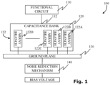
- FIG. 1 indicates selected elements of an electronic system 100 including a functional circuit 110 connected to an array of switched capacitors 122 according to the current disclosure.
- the electronic system 100 includes the functional circuit 110, a capacitance bank 120, a ground plane 130, a noise reduction mechanism 140 and a bias voltage terminal 150. It is particularly noted that the array of switched capacitors 120 is connected to the functional circuit at a single terminal 112 whereas each array branch 122A-D of the capacitance bank 120 is individually connected to the ground plane 130.
- the capacitance bank 120 is a plurality of capacitors mounted upon a substrate.
- the capacitors are arranged into a plurality of capacitor array branches 122A-D having a characteristic capacitance.
- One end of each capacitor array branch 122A-D is connected to a common function circuit terminal 110.
- the other end of each capacitor array branch 122A-D is connected to the ground plane 130 at separate connection points.
- a plurality of electronic switches is provided for selectively connecting each capacitor array branch to the ground plane. Additionally or alternatively, the plurality of electronic switches is provided for selectively connecting each capacitor array branch to the common functional circuit terminal junction.
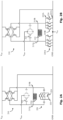
- FIG. 2A an example of a particular functional circuit 210 is shown which is configured as a voltage controlled oscillator (VCO).
- the VCO circuit includes a fine tuning circuit 212 and an inductor element 214.
- the capacitor bank 220 which is used for coarse tuning, is connected between the terminals 215A, 215B of the inductor 214.
- the capacitor bank 220 includes a plurality of array branches 222 each having a different known capacitance each array branch is connected to the ground plane via a corresponding electronic switch 224.
- Required capacitance is selected by switching required the branches such that the overall sum of the capacitance bank is equal to the sum of the individual capacitances of all the selected branches.
- the capacitance of each array branch is a multiple of a power of two such that, where there are N array branches in the bank, 2N discrete values of capacitance are selected.
- FIG. 2B indicates how two arrays 230A, 230B of switched capacitors of the disclosure are incorporated into a similar VCO functional circuit.
- VCO circuit is used for illustrative purposes. It will occur to those skilled in the art that balanced capacitance banks of the disclosure are used with a variety of functional circuits such as, but not limited to phase shifters, filters, tuning circuits and the like.
- the system includes a first capacitance bank 230A connected to a first terminal 215A of the functional circuit 210 and a second capacitance bank 230B connected to a second terminal 215B of the functional circuit 210. It is a particular feature of the system that each array branch 222A of the capacitance bank is connected to a common ground line GND at a separate junction point 223A. Accordingly, the return current path for each branch is different for each branch. Consequently, the capacitance of each branch is controlled.
- ground line itself is biased to a known voltage, such as the true ground, the source supply voltage (VSS), the drain supply voltage (VDD) or the like as suits requirements.
- a known voltage such as the true ground, the source supply voltage (VSS), the drain supply voltage (VDD) or the like as suits requirements.
- Fig. 3 which shows an isometric representation of an extended ground plane 330
- current shaping elements 332 are introduced into the ground plane 330 for equalizing return path current from each array branch 320A, 320B of the capacitance bank.
- Current shaping zones 332 are used to produce a ground plane with a required conductivity map such that the path from each array branch has a required reactance.
- the reactance is selected so as to counteract the deviations from required capacitance for each array branch.
- FIG. 4A schematically represent a particular example of a pair of capacitance arrays 420A, 420B connected to a common current shaping ground plane 430.
- Each capacitance array branch of the example includes a terminal plate 422A, 422B connected to the functional circuit 410 at its center point.
- the terminal plate 422A, 422B is connected to a grounding zone 434A, 434B of the common ground plane 430 via an array of 64 switchable capacitor arranged around its perimeter. It will be appreciated that where each switchable capacitor has the same capacitance C, the capacitor array itself is used to select a total capacitance of any value up to 64C in steps of C by switching the required number of capacitors.
- each switchable capacitor should be equal.
- the various switchable capacitors have different capacitors for example one of the capacitors have a capacitance of C2 such that 128 values of capacitance up to 63.5C are selected in steps of C/2. It will be appreciated that other by providing certain capacitors with other fractional values provide still smaller steps as required. Furthermore, smaller capacitors allow FET switches having smaller sizes to be used. As required central control is provided to subsets of capacitors.
- the common current shaping ground plane has a slot 432 therethrough dividing the grounding zone 434A of the first array 420A with the grounding zone 434B of the second array 420B, thus current flow therebetween is limited such that the return path between the closest capacitors is equal to the return path between the furthest capacitors.
- the array described herein consists of an array of capacitance branches arranged around the perimeter of a rectangle, it will be appreciated that other configurations are preferred as required. For example, circular arrays, spiral arrays, checkerboard arrays, hexagonal arrays, fractal arrays are implemented as suit requirements.
- current forming holes are cut into the metal of the ground plane.
- the current forming holes provide the current shaping zones within the ground plane which direct and shape the return current between each array branch to the bias terminal.
- Such current shaping zones are additionally or alternatively formed by using a ground plane of varying thickness or varying materials. For example, insulating or semiconducting materials are introduced into the ground plane to generate the required resistance map.
- aspects of the present disclosure relate to systems and methods for providing an isolating mechanism for reducing crosstalk between crossing signal lines.
- the disclosure relates to an isolation mechanism introducing a current forming element between the signal carrying lines.
- an isolation mechanism includes current forming elements which set up required currents within the conducting shield such that the reactive component of the inductive coupling cancels the reactive component of the capacitive coupling.
- current directing elements such as shaped holes, insulators, semiconductors or the like are introduced into the conducting shield between the crossing transmission lines. It is noted that shaped holes cut through the metal shield have been found to be particularly effective. This forces the current within the conducting shield to flow around the holes in such as a way that the introduced inductive coupling balances the capacitive coupling reducing crosstalk between the signals.
- shapes for the holes are selected from a group including ellipses, rectangles, triangles, dumbbells, or the like as well as combinations thereof. Accordingly, the dimensions of the hole are determined by suitable selection of defining parameters such as inclination angle, length, width, depth, eccentricity, function of curvature or the like. It is noted that the method is implemented in both single end and differential structures and provides a solution to the crosstalk without adding to overall chip area or complexity. Indeed it is achieved by reducing material from the conducting shield.
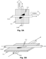
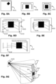
- Figs. 5A and 5B respectively show a top view and an isometric view schematically representing an isolation mechanism 500 according to the disclosure introduced between two crossing single ended signal lines 520A, 520B.
- the signal isolation mechanism for reducing crosstalk between at least two crossing signal lines.
- the system includes a conducting shield 510 a first signal line 520A, a second signal line 520B.
- the conducting shield 510 of the example is an extended conducting plate having a first side (the upperside, say) and a second side (the underside, say).
- the first signal line 520A runs parallel to the upperside side of the conducting shield in a first direction.
- the second signal line 520B runs parallel to the underside of the conducting shield 510 in a second direction not parallel to the first direction. Accordingly, the second signal line 520B crosses the first signal line 520A.
- the conducting shield 510 includes at least one current directing element 512 selected such that inductive coupling generated between the first signal line and the second signal line cancels the capacitive coupling therebetween.
- the current forming element is a hole 512 extending from the first side to the second side of the conductor. It has been found that signal isolation is improved by locating the hole through the conducting shield at the point where the two signals cross along a line extending through the shield from the first signal line to the second signal line.
- the through-hole 512 is shaped such that inductive coupling generated between the first signal line 520A and the second signal line 520B cancels capacitive coupling therebetween. Where appropriate the through-hole 512 is diagonally elongated at an angle to both the first signal line 520A and the second signal line 520B.
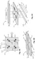
- FIG. 6A, 6B and 6C a top view, an isometric view and an exploded isometric view are shown schematically representing an isolation mechanism 610 introduced between two crossing differential signal lines 620A, 62B according to the current disclosure.
- the first differential signal line 620A comprises a first differential pair of conductors.
- the first differential pair includes a PLUS-line conductor and a MINUS-line conductor.
- the second differential signal 620B line comprises a second differential pair of conductors.
- the second differential pair includes a PLUS-line conductor and a MINUS-line conductor.
- the signal isolation mechanism 610 has a first through hole 612A located along a line through the conducting shield extending from a PLUS-line conductor of the first signal line to a PLUS- line conductor of the second signal line at the point at which they cross.
- the signal isolation mechanism has a second through hole 612B located along a line through the conducting shield extending from a PLUS-line conductor of the first signal line to a MINUS-line conductor of the second signal line at the point at which they cross.
- the signal isolation mechanism has a third through hole 612C located along a line through the conducting shield extending from a MINUS-line conductor of the first signal line to a PLUS-line conductor of the second signal line at the point at which they cross.
- the signal isolation mechanism also has a fourth through hole 612D located along a line through the conducting shield extending from a MINUS-line conductor of the first signal line to a MINUS-line conductor of the second signal line at the point at which they cross.
- couple balancing is improved by shaping and positioning the through holes such that the first through hole is diagonally elongated at a first angle across both the first signal line and the second signal line, the second through hole is diagonally elongated at a second angle across both the first signal line and the second signal line, the third through hole is diagonally elongated at the second angle; and the fourth through hole is diagonally elongated at the first angle.
- hole dimensions and shapes are optimized for particular frequency ranges.
- MIMO arrays are useful and well known concepts to utilize efficiently high-resolution beam-pattern (either by pure digital beamforming or a combination of analog and digital beam-steering).
- some array topologies include an L-shape array 800A, a Pi-shape 800B and a frame-array 800C.
- Such topologies limit the possible attainable system-tradeoffs (such as angular resolution, field-of-view and signal to noise ratio).
- a combined array is a first asymmetric array 800D.
- the asymmetric array is produced by connecting a large number of transmitting ports to wide-beam antennas 812 along a first leg 81 OD of a Pi-shape array and a smaller number of transmitting ports to directional antennas 822 along a second leg 820D of the Pi-shape array.
- the asymmetric array 800D provide most of the high-SNR (signal to noise ratio) and high angular-resolution on the vertical axis of the L-shape array. This produces a wide vertical field-of-view 842 and a narrow vertical field-of-view 848 while doubling the horizontal angular-resolution over a narrow slice 844 in the vertical field-of-view. Accordingly, an enhanced horizontal angular resolution is achieved in a central region 846 of the field-of-view
- the allocation of ports between directional and non-directional antennas is derived from overall system requirements (SNR and resolution over different angular sectors).
- one possible method for obtaining a balanced response from the two asymmetrical branches 810, 820 is by choosing the beamwidth of the directional antennas to be approximately ⁇ ⁇ ⁇ 180° ( N d / N nd ) ⁇ 1 , and antennas-spacing of ( ⁇ /2) ( N nd / N d ) ⁇ 2 , where N d is the number of directional antennas, and N nd is the number of wide-beam antennas, and ⁇ 1 and ⁇ 2 are realization factors.
- Figs. 8E and 8F Other possible embodiments of assymetric arrays are represented in Figs. 8E and 8F .
- a staggered-branch array 800E the directional-antennas are staggered over the vertical-axis. Such an arrangement extends the field-of-view of the staggered branch 820E (grating-lobes rejection).
- the gain and directivity of the receiving antennas and the transmitting antennas are different, and adjusted to optimize system-performance.
- slightly-directional antennas are implemented for the receiving ports - which directivity is between the directional and the non-directional transmitting antennas - D tx,dn ⁇ D rx ⁇ D tx,d .
- a possible transmission-scheme over this topology variously uses a MIMO transmission, or analog-beam forming of the transmitting-antenna, and combine the two transmitting branches either by using time-domain multiplexing (TDM), orthogonal-coding (e.g. Fladamard encoding), frequency-domain multiplexing (FDM, e.g. using different RF frequency per branch) or other methods as required.
- TDM time-domain multiplexing
- orthogonal-coding e.g. Fladamard encoding
- FDM frequency-domain multiplexing
- Still other aspects of the present disclosure relate to the implementation of magneto-electric antennas implemented with common printed circuit board (PCB) technology.
- PCB printed circuit board
- the disclosure relates to providing encapsulated wideband magneto-electric antennas, where the radome is embedded within the antenna design.
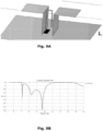
- Fig. 9A is a schematic representation of a magneto-electric dipole antenna which has been found to provide a directional transmission.
- the magneto-electric dipole antenna is a hybrid combination of an electric dipole and a magnetic dipole, which has been shown to generate wideband directional radiation patterns in both the E-plane and the H-plane.
- the magneto-electric dipole antenna includes an electric dipole section, a magnetic dipole section in the form of a magnetic loop and a feed probe.
- the electric dipole section has a first dipole wing section and a second dipole wing section parallel to a ground plane but spaced therefrom by about a half wavelength spacing.
- the magnetic dipole section is formed in a region between the first dipole wing section and the second dipole wing section and is thus bounded on three sides by a first vertical patch section and a second vertical patch section and a connecting patch section of said ground plane.
- the first vertical section connects the ground plane to the first dipole wing section of the electric dipole section and the second vertical section connects the ground plane to the second dipole section.
- the feed probe is situated within the region between the first vertical dipole section and the second vertical dipole section.
- the feed probe is configured and operable to excite the antenna.
- the feed probe includes a gamma-shaped conductor which is connected to an oscillator.
- the gamma-shaped probe has a leg section, a neck section and a folded section the dimensions of which are selected to suit required resistive and capacitive characteristics of the antenna.
- the gain profile for such an antenna is shown in the graph of Fig. 9B which presents the simulated gain profile for such an antenna. It will be noted that the simulated results indicate two resonant reflection zeros within a transmission frequency band of about 6GFHz to 10GFHz.
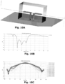
- FIG. 10A a schematic representation is shown of an example of an encapsulated magneto-electric dipole antenna which is used to provide a directional radiation over a wide band of operating frequencies.
- the wideband antenna comprises a magneto-electric dipole including an electric dipole, a magnetic dipole antenna, and a feed probe, all encapsulated inside within a dielectric enclosure.
- the dielectric enclosure is constructed from a glass epoxy material, for example a glass epoxy laminate such as G-10, G-11, FR-4, FR-5 and FR-6 or the like.
- the enclosure is also constructed from magnetic materials having relative magnetic permeability higher than 1.
- the mechanical dimensions of the encapsulated a magneto-electric dipole antenna are significantly smaller than the equivalent air based magneto-electric dipole antenna.
- the flame resistant glass epoxy FR-4 has a relative permittivity Er of 3.8-4 so the wavelength of electromagnetic waves of a given frequency passing therethrough is about half the wavelength of the same frequency radiation in air. Therefore, by encasing a magneto-electric dipole in a dielectric enclosure (like FR-4) the physical dimensions of the antenna are reduced by almost a half.
- the dielectric box dimensions are as small as 18 millimeters x 10 millimeters x 11 millimeters.
- Such a small magneto-electric dipole is readily mounted and stacked upon a PCB for example. At higher frequencies, having shorter wavelength, magneto-electric dipole antennas are suitable for embedding into the PCB or an RFIC package.
- the simulated reflection coefficient over frequency is shown for the antenna of Fig. 10A .
- the air based magneto-electric dipole had only two resonant zeros (see Fig. 9B )
- the dielectric embedded magneto-electric dipole displays three distinct zeros within an extended transmission band of 5.5GHz to 11 GHz.
- the additional resonant zero is a result of the dielectric enclosure serving as a resonant chamber surrounding the antenna formed of dielectric material having a relative permittivity higher than air.
- the graph of Fig. 10C shows how the E-Plane radiation pattern of the antenna of Fig. 10A as a function of frequency between 4 and 10.5GHz.
- the patterns are very stable over frequency in both the E and H planes.
- FIG. 11 illustrates another possible encapsulated magneto-electric dipole antenna designed to be manufactured by standard PCB production processes.
- the wideband antenna again comprises a magneto-electric dipole including an electric dipole, a magnetic dipole antenna, and a feed probe, all encapsulated inside within a dielectric enclosure.
- the magnetic dipole part is not a complete sheet of metal as illustrated in the embodiments above but rather the vertical sections of the magnetic dipole antenna are formed from by a row of platted via holes extending from the ground plane to the dipole wing.
- the feed probe is a gamma-probe including a leg section, a neck section and a folded section, which is similarly formed from vias.
- the leg section comprises a via extending from the ground plane to the bridge section
- the neck section comprises a conducting strip coplanar with the dipole wings
- the folded section comprises a via extending from the neck section towards the ground plane and separated therefrom by an insulator.
- the dielectric enclosure includes a lower section and an upper section.
- the magneto-electric dipole is embedded in the lower section and the upper section comprises a dielectric layer, which is subsequently affixed to cover the lower section. Accordingly, an embedded antenna element is provided which is readily affixed to a printed circuit board.
- a method for manufacturing a wideband antenna includes the following steps: providing a magneto-electric dipole, by providing a pair of horizontal conducting plates spaced so as to serve as two electric dipole wings but leaving a space suitable for a magnetic dipole therebetween; providing a first row of vias extending from a ground plane to a first electric dipole wing to serve as a first vertical section of a magnetic dipole section of the magneto-electric dipole; providing a second row of vias extending from a ground plane to a first electric dipole wing to serve as a second vertical section of a magnetic dipole section of the magneto-electric dipole, and encapsulating the magneto-electric dipole thus constructed in a dielectric material.
- the feed probe is manufactured by providing a conducting strip coplanar with the dipole wings to serve as a neck section of the feed probe; providing a first via extending from the ground plane to the conducting strip section to serve as a leg section of the feed probe; and providing a second via extending from the neck section towards the ground plane and separated therefrom by an insulator to serve as a folded section.
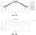
- Fig. 12A shows how the H-Plane gain radiation pattern varies over space angle for frequencies between 4 and 10.5GFHz.
- Fig. 4B shows how the realized gain of the antenna is stable over frequencies between about 5GFHz to 11 GFHz.
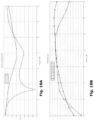
- the graphs of Figs. 13A and 13B illustrate how the simulated results (done using CST Microwave Studio) for the encapsulated magneto-electric dipole antenna of Fig. 11 compare to experimental results for a real encapsulated magneto-electric dipole antenna. It is noted how closely the experimental results follow the expected simulation results.
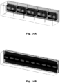
- FIG. 14A a schematic representation is shown of an E-Plane antenna array.
- a row of encapsulated magneto-electric dipole antennas are arranged along a line parallel to their electric dipoles.
- Fig. 14A is a schematic E-Plane cross section representation of the magneto-electric antenna array.
- each antenna is embedded in an individual dielectric lower section, and a common dielectric radome cover caps all antenna of the array, thereby forming an encapsulated array.
- Such an array is manufactured by a method including providing a plurality of magneto-electric dipole antennas, embedding each of the magneto-electric dipole antennas in a dielectric rectangular cuboid , providing a common dielectric radome layer, for all magneto-electric dipole antennas, mounting the embedded magneto-electric dipoles in an array upon a printed circuit board; and covering the array of embedded magneto-electric dipoles with the common dielectric radome layer.
- FIG. 15A shows a schematic representation of an E-Plane antenna array comprising a row of standard electric-dipole antenna arranged along a line parallel to their electric dipoles.
- Fig. 15B is a schematic E-Plane cross section representation of the electric-dipole antenna array.
- Fig. 17A is a schematic representation of an H-Plane antenna array comprising a row of encapsulated magneto-electric dipole antenna arranged along a line orthogonal to their electric dipoles and sharing a common encapsulating radome cap;
- Fig. 17B is a schematic representation of an H-Plane antenna array comprising a row of standard electric-dipole antenna arranged along a line orthogonal to their electric dipoles.
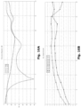
- the behavior of the simulated H-Plane antenna arrays is presented in the graphs of Figs. 18A and 18B are graphs comparing the reflection coefficient and realized gain over wide frequency range for the H- Plane magneto electric antenna array of Fig 17A having a radome layer with a relative permittivity of 3 and a thickness of 2 millimeters, and the H-Plane electric dipole antenna array of Fig 17B.
- composition or method includes additional ingredients and/or steps, but only if the additional ingredients and/or steps do not materially alter the basic and novel characteristics of the claimed composition or method.
- a compound or “at least one compound” includes a plurality of compounds, including mixtures thereof.
- a range such as from 1 to 6 should be considered to have specifically disclosed sub-ranges such as from 1 to 3, from 1 to 4, from 1 to 5, from 2 to 4, from 2 to 6, from 3 to 6 etc., as well as individual numbers within that range, for example, 1, 2, 3, 4, 5, and 6 as well as non-integral intermediate values. This applies regardless of the breadth of the range.
Landscapes
- Engineering & Computer Science (AREA)
- Computer Networks & Wireless Communication (AREA)
- Signal Processing (AREA)
- Power Engineering (AREA)
- Manufacturing & Machinery (AREA)
- Microelectronics & Electronic Packaging (AREA)
- Semiconductor Integrated Circuits (AREA)
- Variable-Direction Aerials And Aerial Arrays (AREA)
Claims (4)
- Array aus geschalteten Kondensatoren (120, 122, 230A, 230B), umfassend:eine Vielzahl von Kondensatoren auf einem Substrat, wobei die Kondensatoren in einer Vielzahl von Kondensatorarrayzweigen (122A-D) angeordnet sind, wobei jeder Kondensatorarrayzweig (122A-D) eine charakteristische Kapazität aufweist; undeine Vielzahl von elektronischen Schaltern, die so konfiguriert sind, dass sie jeden Kondensatorarrayzweig (122A-D) selektiv mit einer erweiterten leitenden Masseebene (130, 330, 430) verbinden,wobei jeder Kondensatorarrayzweig (122A-D) leitend mit einer gemeinsamen funktionalen Schaltungsklemmenabzweigung gekoppelt ist, undwobei die Masseebene (130, 330, 430) mindestens ein Strombegrenzungselement umfasst, das so angeordnet ist, dass Rückstrom von jedem der Kondensatorarrayzweige (122A-D) zu der funktionalen Schaltungsklemmenabzweigung ausgeglichen wird.
- Array aus geschalteten Kondensatoren (120, 122, 230A, 230B) nach Anspruch 1, wobei das mindestens eine Strombegrenzungselement eine Vielzahl von Löchern durch die Masseebene (130, 330, 430) umfasst.
- Array aus geschalteten Kondensatoren (120, 122, 230A, 230B) nach Anspruch 1, wobei das mindestens eine Strombegrenzungselement ein halbleitendes Material umfasst.
- Array aus geschalteten Kondensatoren (120, 122, 230A, 230B) nach Anspruch 1, wobei das mindestens eine Strombegrenzungselement ein isolierendes Material umfasst.
Applications Claiming Priority (5)
| Application Number | Priority Date | Filing Date | Title |
|---|---|---|---|
| US201962924713P | 2019-10-23 | 2019-10-23 | |
| US201962924715P | 2019-10-23 | 2019-10-23 | |
| US201962948332P | 2019-12-16 | 2019-12-16 | |
| US202063011374P | 2020-04-17 | 2020-04-17 | |
| PCT/IB2020/059963 WO2021079325A2 (en) | 2019-10-23 | 2020-10-23 | Systems and methods for improving radio frequency integrated circuits |
Publications (3)
| Publication Number | Publication Date |
|---|---|
| EP4042520A2 EP4042520A2 (de) | 2022-08-17 |
| EP4042520A4 EP4042520A4 (de) | 2023-11-08 |
| EP4042520B1 true EP4042520B1 (de) | 2024-09-04 |
Family
ID=75619409
Family Applications (1)
| Application Number | Title | Priority Date | Filing Date |
|---|---|---|---|
| EP20879560.9A Active EP4042520B1 (de) | 2019-10-23 | 2020-10-23 | Systeme und verfahren zur verbesserung von integrierten hochfrequenzschaltungen |
Country Status (3)
| Country | Link |
|---|---|
| US (1) | US11329732B1 (de) |
| EP (1) | EP4042520B1 (de) |
| WO (1) | WO2021079325A2 (de) |
Families Citing this family (1)
| Publication number | Priority date | Publication date | Assignee | Title |
|---|---|---|---|---|
| US12040537B2 (en) * | 2021-05-19 | 2024-07-16 | Fuba Automotive Electronics Gmbh | Radiation coupled antennas with network |
Family Cites Families (13)
| Publication number | Priority date | Publication date | Assignee | Title |
|---|---|---|---|---|
| FR2768852B1 (fr) * | 1997-09-22 | 1999-11-26 | Sgs Thomson Microelectronics | Realisation d'un condensateur intermetallique |
| US7555263B1 (en) * | 1999-10-21 | 2009-06-30 | Broadcom Corporation | Adaptive radio transceiver |
| US6903946B1 (en) | 2003-11-04 | 2005-06-07 | Lockheed Martin Corporation | Paralleled power factor correcting AC-to-DC converters with improved current balance |
| TWI373925B (en) * | 2004-02-10 | 2012-10-01 | Tridev Res L L C | Tunable resonant circuit, tunable voltage controlled oscillator circuit, tunable low noise amplifier circuit and method of tuning a resonant circuit |
| US8421556B2 (en) * | 2009-10-16 | 2013-04-16 | Broadcom Corporation | Switched capacitor array having reduced parasitics |
| US8791767B2 (en) * | 2010-10-29 | 2014-07-29 | Qualcomm Incorporated | Package inductance compensating tunable capacitor circuit |
| FR2975803B1 (fr) | 2011-05-24 | 2014-01-10 | Commissariat Energie Atomique | Circuit integre realise en soi comprenant des cellules adjacentes de differents types |
| CN104704682B (zh) * | 2012-08-22 | 2017-03-22 | 安费诺有限公司 | 高频电连接器 |
| US20140065982A1 (en) * | 2012-09-05 | 2014-03-06 | Seong-Youp Suh | Plug-and-play time-variant antenna module for wireless communication devices |
| US9496902B2 (en) * | 2014-07-24 | 2016-11-15 | Skyworks Solutions, Inc. | Apparatus and methods for reconfigurable directional couplers in an RF transceiver with selectable phase shifters |
| US10679823B2 (en) * | 2015-02-18 | 2020-06-09 | Reno Technologies, Inc. | Switching circuit |
| JP2017103333A (ja) * | 2015-12-01 | 2017-06-08 | 三菱重工業株式会社 | 回路基板及びその製造方法 |
| US10951202B2 (en) * | 2018-07-20 | 2021-03-16 | Futurewei Technologies, Inc. | Method and apparatus for RC/CR phase error calibration of measurement receiver |
-
2020
- 2020-10-23 WO PCT/IB2020/059963 patent/WO2021079325A2/en not_active Ceased
- 2020-10-23 US US17/606,775 patent/US11329732B1/en active Active
- 2020-10-23 EP EP20879560.9A patent/EP4042520B1/de active Active
Also Published As
| Publication number | Publication date |
|---|---|
| US11329732B1 (en) | 2022-05-10 |
| EP4042520A2 (de) | 2022-08-17 |
| WO2021079325A2 (en) | 2021-04-29 |
| WO2021079325A3 (en) | 2021-07-01 |
| EP4042520A4 (de) | 2023-11-08 |
| US20220149957A1 (en) | 2022-05-12 |
Similar Documents
| Publication | Publication Date | Title |
|---|---|---|
| Zhou et al. | Triband dual-polarized shared-aperture antenna for 2G/3G/4G/5G base station applications | |
| US9548544B2 (en) | Antenna element for signals with three polarizations | |
| CN108352599B (zh) | 适用于基站天线的天线元件 | |
| US8466846B1 (en) | Ultra wide band balanced antipodal tapered slot antenna and array with edge treatment | |
| US7932869B2 (en) | Antenna with volume of material | |
| US8830135B2 (en) | Dipole antenna element with independently tunable sleeve | |
| EP3662537B1 (de) | Dreipol-stromschleifenstrahlelement mit integrierter zirkular polarisierter speisung | |
| CN112201965A (zh) | 利用人工磁导体的阵列天线 | |
| WO2005067549A2 (en) | Multi frequency magnetic dipole antenna structures and methods of reusing the volume of an antenna | |
| US20170149145A1 (en) | Cross-Dipole Antenna Configurations | |
| Zheng et al. | A miniaturized wideband dual-polarized antenna based on mode-control principle for base-station applications | |
| JP2002151942A (ja) | 固定通信用の平面状アンテナ及びそのアンテナのエラーを補償する方法 | |
| Kiani et al. | Wideband three loop element antenna array for future 5G mmWave devices | |
| JP6678617B2 (ja) | 円偏波アンテナ | |
| Wang et al. | A novel differential filtering patch antenna with high selectivity | |
| EP4042520B1 (de) | Systeme und verfahren zur verbesserung von integrierten hochfrequenzschaltungen | |
| KR102354525B1 (ko) | 고이득 세그멘티드 패치 안테나 및 그 제조방법 | |
| Chen et al. | Dual-beam microstrip leaky-wave array excited by aperture-coupling method | |
| JP6678616B2 (ja) | 両偏波送受用アンテナ | |
| JP3896331B2 (ja) | 円偏波パッチアンテナ | |
| US10170829B2 (en) | Self-complementary multilayer array antenna | |
| EP3280006A1 (de) | Doppelt polarisierte antenne | |
| Lu et al. | Dual‐polarized stacked microstrip antenna with trident‐shaped baluns for MIMO array development | |
| Yang et al. | Wideband phase-reversal antenna using a novel bandwidth enhancement technique | |
| WO2007106976A1 (en) | Tri-polar antenna array element |
Legal Events
| Date | Code | Title | Description |
|---|---|---|---|
| STAA | Information on the status of an ep patent application or granted ep patent |
Free format text: STATUS: THE INTERNATIONAL PUBLICATION HAS BEEN MADE |
|
| PUAI | Public reference made under article 153(3) epc to a published international application that has entered the european phase |
Free format text: ORIGINAL CODE: 0009012 |
|
| STAA | Information on the status of an ep patent application or granted ep patent |
Free format text: STATUS: REQUEST FOR EXAMINATION WAS MADE |
|
| 17P | Request for examination filed |
Effective date: 20220510 |
|
| AK | Designated contracting states |
Kind code of ref document: A2 Designated state(s): AL AT BE BG CH CY CZ DE DK EE ES FI FR GB GR HR HU IE IS IT LI LT LU LV MC MK MT NL NO PL PT RO RS SE SI SK SM TR |
|
| DAV | Request for validation of the european patent (deleted) | ||
| DAX | Request for extension of the european patent (deleted) | ||
| A4 | Supplementary search report drawn up and despatched |
Effective date: 20231009 |
|
| RIC1 | Information provided on ipc code assigned before grant |
Ipc: H04B 15/04 20060101ALI20231003BHEP Ipc: H01L 23/66 20060101ALI20231003BHEP Ipc: H01G 4/40 20060101ALI20231003BHEP Ipc: H01G 4/38 20060101ALI20231003BHEP Ipc: H01L 23/552 20060101ALI20231003BHEP Ipc: H03H 7/00 20060101ALI20231003BHEP Ipc: H01R 13/6467 20110101ALI20231003BHEP Ipc: H01R 13/6461 20110101AFI20231003BHEP |
|
| GRAP | Despatch of communication of intention to grant a patent |
Free format text: ORIGINAL CODE: EPIDOSNIGR1 |
|
| STAA | Information on the status of an ep patent application or granted ep patent |
Free format text: STATUS: GRANT OF PATENT IS INTENDED |
|
| GRAJ | Information related to disapproval of communication of intention to grant by the applicant or resumption of examination proceedings by the epo deleted |
Free format text: ORIGINAL CODE: EPIDOSDIGR1 |
|
| STAA | Information on the status of an ep patent application or granted ep patent |
Free format text: STATUS: REQUEST FOR EXAMINATION WAS MADE |
|
| INTG | Intention to grant announced |
Effective date: 20240426 |
|
| INTC | Intention to grant announced (deleted) | ||
| GRAP | Despatch of communication of intention to grant a patent |
Free format text: ORIGINAL CODE: EPIDOSNIGR1 |
|
| STAA | Information on the status of an ep patent application or granted ep patent |
Free format text: STATUS: GRANT OF PATENT IS INTENDED |
|
| INTG | Intention to grant announced |
Effective date: 20240612 |
|
| GRAS | Grant fee paid |
Free format text: ORIGINAL CODE: EPIDOSNIGR3 |
|
| GRAA | (expected) grant |
Free format text: ORIGINAL CODE: 0009210 |
|
| STAA | Information on the status of an ep patent application or granted ep patent |
Free format text: STATUS: THE PATENT HAS BEEN GRANTED |
|
| AK | Designated contracting states |
Kind code of ref document: B1 Designated state(s): AL AT BE BG CH CY CZ DE DK EE ES FI FR GB GR HR HU IE IS IT LI LT LU LV MC MK MT NL NO PL PT RO RS SE SI SK SM TR |
|
| REG | Reference to a national code |
Ref country code: GB Ref legal event code: FG4D |
|
| REG | Reference to a national code |
Ref country code: CH Ref legal event code: EP |
|
| REG | Reference to a national code |
Ref country code: IE Ref legal event code: FG4D |
|
| REG | Reference to a national code |
Ref country code: DE Ref legal event code: R096 Ref document number: 602020037309 Country of ref document: DE |
|
| REG | Reference to a national code |
Ref country code: LT Ref legal event code: MG9D |
|
| REG | Reference to a national code |
Ref country code: NL Ref legal event code: MP Effective date: 20240904 |
|
| PG25 | Lapsed in a contracting state [announced via postgrant information from national office to epo] |
Ref country code: NO Free format text: LAPSE BECAUSE OF FAILURE TO SUBMIT A TRANSLATION OF THE DESCRIPTION OR TO PAY THE FEE WITHIN THE PRESCRIBED TIME-LIMIT Effective date: 20241204 |
|
| PG25 | Lapsed in a contracting state [announced via postgrant information from national office to epo] |
Ref country code: GR Free format text: LAPSE BECAUSE OF FAILURE TO SUBMIT A TRANSLATION OF THE DESCRIPTION OR TO PAY THE FEE WITHIN THE PRESCRIBED TIME-LIMIT Effective date: 20241205 Ref country code: PL Free format text: LAPSE BECAUSE OF FAILURE TO SUBMIT A TRANSLATION OF THE DESCRIPTION OR TO PAY THE FEE WITHIN THE PRESCRIBED TIME-LIMIT Effective date: 20240904 Ref country code: FI Free format text: LAPSE BECAUSE OF FAILURE TO SUBMIT A TRANSLATION OF THE DESCRIPTION OR TO PAY THE FEE WITHIN THE PRESCRIBED TIME-LIMIT Effective date: 20240904 |
|
| PG25 | Lapsed in a contracting state [announced via postgrant information from national office to epo] |
Ref country code: BG Free format text: LAPSE BECAUSE OF FAILURE TO SUBMIT A TRANSLATION OF THE DESCRIPTION OR TO PAY THE FEE WITHIN THE PRESCRIBED TIME-LIMIT Effective date: 20240904 |
|
| PG25 | Lapsed in a contracting state [announced via postgrant information from national office to epo] |
Ref country code: LV Free format text: LAPSE BECAUSE OF FAILURE TO SUBMIT A TRANSLATION OF THE DESCRIPTION OR TO PAY THE FEE WITHIN THE PRESCRIBED TIME-LIMIT Effective date: 20240904 |
|
| PG25 | Lapsed in a contracting state [announced via postgrant information from national office to epo] |
Ref country code: HR Free format text: LAPSE BECAUSE OF FAILURE TO SUBMIT A TRANSLATION OF THE DESCRIPTION OR TO PAY THE FEE WITHIN THE PRESCRIBED TIME-LIMIT Effective date: 20240904 |
|
| PG25 | Lapsed in a contracting state [announced via postgrant information from national office to epo] |
Ref country code: ES Free format text: LAPSE BECAUSE OF FAILURE TO SUBMIT A TRANSLATION OF THE DESCRIPTION OR TO PAY THE FEE WITHIN THE PRESCRIBED TIME-LIMIT Effective date: 20240904 Ref country code: RS Free format text: LAPSE BECAUSE OF FAILURE TO SUBMIT A TRANSLATION OF THE DESCRIPTION OR TO PAY THE FEE WITHIN THE PRESCRIBED TIME-LIMIT Effective date: 20241204 |
|
| PG25 | Lapsed in a contracting state [announced via postgrant information from national office to epo] |
Ref country code: RS Free format text: LAPSE BECAUSE OF FAILURE TO SUBMIT A TRANSLATION OF THE DESCRIPTION OR TO PAY THE FEE WITHIN THE PRESCRIBED TIME-LIMIT Effective date: 20241204 Ref country code: PL Free format text: LAPSE BECAUSE OF FAILURE TO SUBMIT A TRANSLATION OF THE DESCRIPTION OR TO PAY THE FEE WITHIN THE PRESCRIBED TIME-LIMIT Effective date: 20240904 Ref country code: NO Free format text: LAPSE BECAUSE OF FAILURE TO SUBMIT A TRANSLATION OF THE DESCRIPTION OR TO PAY THE FEE WITHIN THE PRESCRIBED TIME-LIMIT Effective date: 20241204 Ref country code: LV Free format text: LAPSE BECAUSE OF FAILURE TO SUBMIT A TRANSLATION OF THE DESCRIPTION OR TO PAY THE FEE WITHIN THE PRESCRIBED TIME-LIMIT Effective date: 20240904 Ref country code: HR Free format text: LAPSE BECAUSE OF FAILURE TO SUBMIT A TRANSLATION OF THE DESCRIPTION OR TO PAY THE FEE WITHIN THE PRESCRIBED TIME-LIMIT Effective date: 20240904 Ref country code: GR Free format text: LAPSE BECAUSE OF FAILURE TO SUBMIT A TRANSLATION OF THE DESCRIPTION OR TO PAY THE FEE WITHIN THE PRESCRIBED TIME-LIMIT Effective date: 20241205 Ref country code: FI Free format text: LAPSE BECAUSE OF FAILURE TO SUBMIT A TRANSLATION OF THE DESCRIPTION OR TO PAY THE FEE WITHIN THE PRESCRIBED TIME-LIMIT Effective date: 20240904 Ref country code: ES Free format text: LAPSE BECAUSE OF FAILURE TO SUBMIT A TRANSLATION OF THE DESCRIPTION OR TO PAY THE FEE WITHIN THE PRESCRIBED TIME-LIMIT Effective date: 20240904 Ref country code: BG Free format text: LAPSE BECAUSE OF FAILURE TO SUBMIT A TRANSLATION OF THE DESCRIPTION OR TO PAY THE FEE WITHIN THE PRESCRIBED TIME-LIMIT Effective date: 20240904 |
|
| REG | Reference to a national code |
Ref country code: AT Ref legal event code: MK05 Ref document number: 1721410 Country of ref document: AT Kind code of ref document: T Effective date: 20240904 |
|
| PG25 | Lapsed in a contracting state [announced via postgrant information from national office to epo] |
Ref country code: NL Free format text: LAPSE BECAUSE OF FAILURE TO SUBMIT A TRANSLATION OF THE DESCRIPTION OR TO PAY THE FEE WITHIN THE PRESCRIBED TIME-LIMIT Effective date: 20240904 |
|
| PG25 | Lapsed in a contracting state [announced via postgrant information from national office to epo] |
Ref country code: PT Free format text: LAPSE BECAUSE OF FAILURE TO SUBMIT A TRANSLATION OF THE DESCRIPTION OR TO PAY THE FEE WITHIN THE PRESCRIBED TIME-LIMIT Effective date: 20250106 Ref country code: IS Free format text: LAPSE BECAUSE OF FAILURE TO SUBMIT A TRANSLATION OF THE DESCRIPTION OR TO PAY THE FEE WITHIN THE PRESCRIBED TIME-LIMIT Effective date: 20250104 |
|
| PG25 | Lapsed in a contracting state [announced via postgrant information from national office to epo] |
Ref country code: RO Free format text: LAPSE BECAUSE OF FAILURE TO SUBMIT A TRANSLATION OF THE DESCRIPTION OR TO PAY THE FEE WITHIN THE PRESCRIBED TIME-LIMIT Effective date: 20240904 Ref country code: SM Free format text: LAPSE BECAUSE OF FAILURE TO SUBMIT A TRANSLATION OF THE DESCRIPTION OR TO PAY THE FEE WITHIN THE PRESCRIBED TIME-LIMIT Effective date: 20240904 |
|
| PG25 | Lapsed in a contracting state [announced via postgrant information from national office to epo] |
Ref country code: EE Free format text: LAPSE BECAUSE OF FAILURE TO SUBMIT A TRANSLATION OF THE DESCRIPTION OR TO PAY THE FEE WITHIN THE PRESCRIBED TIME-LIMIT Effective date: 20240904 Ref country code: AT Free format text: LAPSE BECAUSE OF FAILURE TO SUBMIT A TRANSLATION OF THE DESCRIPTION OR TO PAY THE FEE WITHIN THE PRESCRIBED TIME-LIMIT Effective date: 20240904 |
|
| PG25 | Lapsed in a contracting state [announced via postgrant information from national office to epo] |
Ref country code: CZ Free format text: LAPSE BECAUSE OF FAILURE TO SUBMIT A TRANSLATION OF THE DESCRIPTION OR TO PAY THE FEE WITHIN THE PRESCRIBED TIME-LIMIT Effective date: 20240904 |
|
| PG25 | Lapsed in a contracting state [announced via postgrant information from national office to epo] |
Ref country code: SK Free format text: LAPSE BECAUSE OF FAILURE TO SUBMIT A TRANSLATION OF THE DESCRIPTION OR TO PAY THE FEE WITHIN THE PRESCRIBED TIME-LIMIT Effective date: 20240904 Ref country code: IT Free format text: LAPSE BECAUSE OF FAILURE TO SUBMIT A TRANSLATION OF THE DESCRIPTION OR TO PAY THE FEE WITHIN THE PRESCRIBED TIME-LIMIT Effective date: 20240904 |
|
| REG | Reference to a national code |
Ref country code: CH Ref legal event code: PL |
|
| REG | Reference to a national code |
Ref country code: DE Ref legal event code: R097 Ref document number: 602020037309 Country of ref document: DE |
|
| PG25 | Lapsed in a contracting state [announced via postgrant information from national office to epo] |
Ref country code: MC Free format text: LAPSE BECAUSE OF FAILURE TO SUBMIT A TRANSLATION OF THE DESCRIPTION OR TO PAY THE FEE WITHIN THE PRESCRIBED TIME-LIMIT Effective date: 20240904 |
|
| PGFP | Annual fee paid to national office [announced via postgrant information from national office to epo] |
Ref country code: DE Payment date: 20250430 Year of fee payment: 5 |
|
| PG25 | Lapsed in a contracting state [announced via postgrant information from national office to epo] |
Ref country code: DK Free format text: LAPSE BECAUSE OF FAILURE TO SUBMIT A TRANSLATION OF THE DESCRIPTION OR TO PAY THE FEE WITHIN THE PRESCRIBED TIME-LIMIT Effective date: 20240904 |
|
| PLBE | No opposition filed within time limit |
Free format text: ORIGINAL CODE: 0009261 |
|
| STAA | Information on the status of an ep patent application or granted ep patent |
Free format text: STATUS: NO OPPOSITION FILED WITHIN TIME LIMIT |
|
| PG25 | Lapsed in a contracting state [announced via postgrant information from national office to epo] |
Ref country code: BE Free format text: LAPSE BECAUSE OF NON-PAYMENT OF DUE FEES Effective date: 20241031 Ref country code: LU Free format text: LAPSE BECAUSE OF NON-PAYMENT OF DUE FEES Effective date: 20241023 |
|
| PGFP | Annual fee paid to national office [announced via postgrant information from national office to epo] |
Ref country code: FR Payment date: 20250430 Year of fee payment: 5 |
|
| PG25 | Lapsed in a contracting state [announced via postgrant information from national office to epo] |
Ref country code: CH Free format text: LAPSE BECAUSE OF NON-PAYMENT OF DUE FEES Effective date: 20241031 |
|
| REG | Reference to a national code |
Ref country code: BE Ref legal event code: MM Effective date: 20241031 |
|
| 26N | No opposition filed |
Effective date: 20250605 |
|
| GBPC | Gb: european patent ceased through non-payment of renewal fee |
Effective date: 20241204 |
|
| PG25 | Lapsed in a contracting state [announced via postgrant information from national office to epo] |
Ref country code: SE Free format text: LAPSE BECAUSE OF FAILURE TO SUBMIT A TRANSLATION OF THE DESCRIPTION OR TO PAY THE FEE WITHIN THE PRESCRIBED TIME-LIMIT Effective date: 20240904 |
|
| PG25 | Lapsed in a contracting state [announced via postgrant information from national office to epo] |
Ref country code: GB Free format text: LAPSE BECAUSE OF NON-PAYMENT OF DUE FEES Effective date: 20241204 |
|
| PG25 | Lapsed in a contracting state [announced via postgrant information from national office to epo] |
Ref country code: IE Free format text: LAPSE BECAUSE OF NON-PAYMENT OF DUE FEES Effective date: 20241023 |
|
| PG25 | Lapsed in a contracting state [announced via postgrant information from national office to epo] |
Ref country code: CY Free format text: LAPSE BECAUSE OF FAILURE TO SUBMIT A TRANSLATION OF THE DESCRIPTION OR TO PAY THE FEE WITHIN THE PRESCRIBED TIME-LIMIT; INVALID AB INITIO Effective date: 20201023 |
|
| PG25 | Lapsed in a contracting state [announced via postgrant information from national office to epo] |
Ref country code: HU Free format text: LAPSE BECAUSE OF FAILURE TO SUBMIT A TRANSLATION OF THE DESCRIPTION OR TO PAY THE FEE WITHIN THE PRESCRIBED TIME-LIMIT; INVALID AB INITIO Effective date: 20201023 |