EP4043135A1 - Elektrodendraht für eine elektroerosivbearbeitung - Google Patents
Elektrodendraht für eine elektroerosivbearbeitung Download PDFInfo
- Publication number
- EP4043135A1 EP4043135A1 EP20871898.1A EP20871898A EP4043135A1 EP 4043135 A1 EP4043135 A1 EP 4043135A1 EP 20871898 A EP20871898 A EP 20871898A EP 4043135 A1 EP4043135 A1 EP 4043135A1
- Authority
- EP
- European Patent Office
- Prior art keywords
- phase
- electrode wire
- electrical discharge
- discharge machining
- alloy layer
- Prior art date
- Legal status (The legal status is an assumption and is not a legal conclusion. Google has not performed a legal analysis and makes no representation as to the accuracy of the status listed.)
- Pending
Links
- 238000009760 electrical discharge machining Methods 0.000 title claims abstract description 59
- 229910045601 alloy Inorganic materials 0.000 claims abstract description 58
- 239000000956 alloy Substances 0.000 claims abstract description 58
- 229910052751 metal Inorganic materials 0.000 claims abstract description 24
- 239000002184 metal Substances 0.000 claims abstract description 24
- 239000006185 dispersion Substances 0.000 claims abstract description 20
- 239000010410 layer Substances 0.000 claims description 82
- 239000011701 zinc Substances 0.000 claims description 26
- 239000010949 copper Substances 0.000 claims description 23
- HCHKCACWOHOZIP-UHFFFAOYSA-N Zinc Chemical compound [Zn] HCHKCACWOHOZIP-UHFFFAOYSA-N 0.000 claims description 20
- 229910052725 zinc Inorganic materials 0.000 claims description 20
- RYGMFSIKBFXOCR-UHFFFAOYSA-N Copper Chemical compound [Cu] RYGMFSIKBFXOCR-UHFFFAOYSA-N 0.000 claims description 18
- 229910052802 copper Inorganic materials 0.000 claims description 17
- 239000002344 surface layer Substances 0.000 claims description 17
- 229920000642 polymer Polymers 0.000 claims description 14
- 239000002322 conducting polymer Substances 0.000 claims description 10
- 229920001940 conductive polymer Polymers 0.000 claims description 10
- 229910001369 Brass Inorganic materials 0.000 claims description 9
- 239000010951 brass Substances 0.000 claims description 9
- ATJFFYVFTNAWJD-UHFFFAOYSA-N Tin Chemical compound [Sn] ATJFFYVFTNAWJD-UHFFFAOYSA-N 0.000 claims description 3
- 229910052782 aluminium Inorganic materials 0.000 claims description 3
- XAGFODPZIPBFFR-UHFFFAOYSA-N aluminium Chemical compound [Al] XAGFODPZIPBFFR-UHFFFAOYSA-N 0.000 claims description 3
- 229910052718 tin Inorganic materials 0.000 claims description 3
- 238000003754 machining Methods 0.000 abstract description 36
- 230000003746 surface roughness Effects 0.000 abstract description 13
- 238000000034 method Methods 0.000 description 20
- 238000010438 heat treatment Methods 0.000 description 17
- 208000028659 discharge Diseases 0.000 description 15
- 230000000694 effects Effects 0.000 description 13
- TVZPLCNGKSPOJA-UHFFFAOYSA-N copper zinc Chemical compound [Cu].[Zn] TVZPLCNGKSPOJA-UHFFFAOYSA-N 0.000 description 11
- 238000004519 manufacturing process Methods 0.000 description 11
- 238000001816 cooling Methods 0.000 description 10
- 238000007747 plating Methods 0.000 description 10
- 230000008569 process Effects 0.000 description 10
- RZJQYRCNDBMIAG-UHFFFAOYSA-N [Cu].[Cu].[Cu].[Cu].[Cu].[Cu].[Cu].[Cu].[Cu].[Cu].[Cu].[Cu].[Cu].[Cu].[Cu].[Cu].[Cu].[Cu].[Zn].[Ag].[Ag].[Ag].[Ag].[Ag].[Ag].[Ag].[Ag].[Ag].[Ag].[Ag].[Ag].[Ag].[Ag].[Ag].[Ag].[Ag].[Ag].[Ag].[Ag].[Ag].[Ag].[Ag].[Ag].[Ag].[Ag].[Ag].[Ag].[Ag].[Ag].[Ag].[Ag].[Ag].[Ag].[Ag].[Ag].[Ag].[Ag].[Ag].[Ag].[Ag].[Ag].[Ag].[Ag].[Ag].[Ag].[Ag].[Ag].[Ag].[Ag].[Ag].[Ag].[Ag].[Ag].[Ag].[Ag].[Ag].[Ag].[Ag].[Ag].[Ag].[Ag].[Sn].[Sn].[Sn].[Sn].[Sn].[Sn].[Sn].[Sn].[Sn].[Sn].[Sn].[Sn].[Sn].[Sn].[Sn].[Sn].[Sn].[Sn] Chemical class [Cu].[Cu].[Cu].[Cu].[Cu].[Cu].[Cu].[Cu].[Cu].[Cu].[Cu].[Cu].[Cu].[Cu].[Cu].[Cu].[Cu].[Cu].[Zn].[Ag].[Ag].[Ag].[Ag].[Ag].[Ag].[Ag].[Ag].[Ag].[Ag].[Ag].[Ag].[Ag].[Ag].[Ag].[Ag].[Ag].[Ag].[Ag].[Ag].[Ag].[Ag].[Ag].[Ag].[Ag].[Ag].[Ag].[Ag].[Ag].[Ag].[Ag].[Ag].[Ag].[Ag].[Ag].[Ag].[Ag].[Ag].[Ag].[Ag].[Ag].[Ag].[Ag].[Ag].[Ag].[Ag].[Ag].[Ag].[Ag].[Ag].[Ag].[Ag].[Ag].[Ag].[Ag].[Ag].[Ag].[Ag].[Ag].[Ag].[Ag].[Ag].[Sn].[Sn].[Sn].[Sn].[Sn].[Sn].[Sn].[Sn].[Sn].[Sn].[Sn].[Sn].[Sn].[Sn].[Sn].[Sn].[Sn].[Sn] RZJQYRCNDBMIAG-UHFFFAOYSA-N 0.000 description 8
- 238000005516 engineering process Methods 0.000 description 8
- 238000002309 gasification Methods 0.000 description 8
- 238000010587 phase diagram Methods 0.000 description 8
- 229910001297 Zn alloy Inorganic materials 0.000 description 7
- 230000000052 comparative effect Effects 0.000 description 7
- 238000012360 testing method Methods 0.000 description 7
- 229910017518 Cu Zn Inorganic materials 0.000 description 6
- 229910017752 Cu-Zn Inorganic materials 0.000 description 6
- 229910017943 Cu—Zn Inorganic materials 0.000 description 6
- XEEYBQQBJWHFJM-UHFFFAOYSA-N Iron Chemical compound [Fe] XEEYBQQBJWHFJM-UHFFFAOYSA-N 0.000 description 6
- 239000000498 cooling water Substances 0.000 description 6
- 229910002056 binary alloy Inorganic materials 0.000 description 4
- 238000005260 corrosion Methods 0.000 description 4
- 230000007797 corrosion Effects 0.000 description 4
- 239000012634 fragment Substances 0.000 description 4
- 238000005246 galvanizing Methods 0.000 description 4
- 230000006872 improvement Effects 0.000 description 4
- 229920000767 polyaniline Polymers 0.000 description 4
- 238000009713 electroplating Methods 0.000 description 3
- 229910052742 iron Inorganic materials 0.000 description 3
- FAPWRFPIFSIZLT-UHFFFAOYSA-M Sodium chloride Chemical compound [Na+].[Cl-] FAPWRFPIFSIZLT-UHFFFAOYSA-M 0.000 description 2
- 229910000831 Steel Inorganic materials 0.000 description 2
- 230000008859 change Effects 0.000 description 2
- 239000011248 coating agent Substances 0.000 description 2
- 238000000576 coating method Methods 0.000 description 2
- 238000005520 cutting process Methods 0.000 description 2
- 238000010586 diagram Methods 0.000 description 2
- 230000002401 inhibitory effect Effects 0.000 description 2
- 239000012212 insulator Substances 0.000 description 2
- 230000001788 irregular Effects 0.000 description 2
- 239000000463 material Substances 0.000 description 2
- 230000003449 preventive effect Effects 0.000 description 2
- 239000004065 semiconductor Substances 0.000 description 2
- 239000010959 steel Substances 0.000 description 2
- 238000009763 wire-cut EDM Methods 0.000 description 2
- WKBPZYKAUNRMKP-UHFFFAOYSA-N 1-[2-(2,4-dichlorophenyl)pentyl]1,2,4-triazole Chemical compound C=1C=C(Cl)C=C(Cl)C=1C(CCC)CN1C=NC=N1 WKBPZYKAUNRMKP-UHFFFAOYSA-N 0.000 description 1
- IJGRMHOSHXDMSA-UHFFFAOYSA-N Atomic nitrogen Chemical compound N#N IJGRMHOSHXDMSA-UHFFFAOYSA-N 0.000 description 1
- ZAMOUSCENKQFHK-UHFFFAOYSA-N Chlorine atom Chemical compound [Cl] ZAMOUSCENKQFHK-UHFFFAOYSA-N 0.000 description 1
- 229910000881 Cu alloy Inorganic materials 0.000 description 1
- ZOKXTWBITQBERF-UHFFFAOYSA-N Molybdenum Chemical compound [Mo] ZOKXTWBITQBERF-UHFFFAOYSA-N 0.000 description 1
- 229920001609 Poly(3,4-ethylenedioxythiophene) Polymers 0.000 description 1
- 229910001315 Tool steel Inorganic materials 0.000 description 1
- 238000010521 absorption reaction Methods 0.000 description 1
- 230000008901 benefit Effects 0.000 description 1
- 238000006243 chemical reaction Methods 0.000 description 1
- 239000000460 chlorine Substances 0.000 description 1
- 229910052801 chlorine Inorganic materials 0.000 description 1
- 238000005336 cracking Methods 0.000 description 1
- 230000007423 decrease Effects 0.000 description 1
- 230000000593 degrading effect Effects 0.000 description 1
- 229910003460 diamond Inorganic materials 0.000 description 1
- 239000010432 diamond Substances 0.000 description 1
- 229910001873 dinitrogen Inorganic materials 0.000 description 1
- 238000002474 experimental method Methods 0.000 description 1
- 239000007788 liquid Substances 0.000 description 1
- 239000000203 mixture Substances 0.000 description 1
- 229910052750 molybdenum Inorganic materials 0.000 description 1
- 239000011733 molybdenum Substances 0.000 description 1
- 230000001590 oxidative effect Effects 0.000 description 1
- 239000011780 sodium chloride Substances 0.000 description 1
- 239000007921 spray Substances 0.000 description 1
- 238000005507 spraying Methods 0.000 description 1
- 230000006641 stabilisation Effects 0.000 description 1
- 238000011105 stabilization Methods 0.000 description 1
- 230000000087 stabilizing effect Effects 0.000 description 1
- WFKWXMTUELFFGS-UHFFFAOYSA-N tungsten Chemical compound [W] WFKWXMTUELFFGS-UHFFFAOYSA-N 0.000 description 1
- 229910052721 tungsten Inorganic materials 0.000 description 1
- 239000010937 tungsten Substances 0.000 description 1
- 239000011800 void material Substances 0.000 description 1
- XLYOFNOQVPJJNP-UHFFFAOYSA-N water Substances O XLYOFNOQVPJJNP-UHFFFAOYSA-N 0.000 description 1
Images


Classifications
-
- B—PERFORMING OPERATIONS; TRANSPORTING
- B23—MACHINE TOOLS; METAL-WORKING NOT OTHERWISE PROVIDED FOR
- B23H—WORKING OF METAL BY THE ACTION OF A HIGH CONCENTRATION OF ELECTRIC CURRENT ON A WORKPIECE USING AN ELECTRODE WHICH TAKES THE PLACE OF A TOOL; SUCH WORKING COMBINED WITH OTHER FORMS OF WORKING OF METAL
- B23H1/00—Electrical discharge machining, i.e. removing metal with a series of rapidly recurring electrical discharges between an electrode and a workpiece in the presence of a fluid dielectric
- B23H1/04—Electrodes specially adapted therefor or their manufacture
-
- B—PERFORMING OPERATIONS; TRANSPORTING
- B23—MACHINE TOOLS; METAL-WORKING NOT OTHERWISE PROVIDED FOR
- B23H—WORKING OF METAL BY THE ACTION OF A HIGH CONCENTRATION OF ELECTRIC CURRENT ON A WORKPIECE USING AN ELECTRODE WHICH TAKES THE PLACE OF A TOOL; SUCH WORKING COMBINED WITH OTHER FORMS OF WORKING OF METAL
- B23H7/00—Processes or apparatus applicable to both electrical discharge machining and electrochemical machining
- B23H7/02—Wire-cutting
- B23H7/08—Wire electrodes
-
- B—PERFORMING OPERATIONS; TRANSPORTING
- B23—MACHINE TOOLS; METAL-WORKING NOT OTHERWISE PROVIDED FOR
- B23H—WORKING OF METAL BY THE ACTION OF A HIGH CONCENTRATION OF ELECTRIC CURRENT ON A WORKPIECE USING AN ELECTRODE WHICH TAKES THE PLACE OF A TOOL; SUCH WORKING COMBINED WITH OTHER FORMS OF WORKING OF METAL
- B23H1/00—Electrical discharge machining, i.e. removing metal with a series of rapidly recurring electrical discharges between an electrode and a workpiece in the presence of a fluid dielectric
- B23H1/04—Electrodes specially adapted therefor or their manufacture
- B23H1/06—Electrode material
-
- C—CHEMISTRY; METALLURGY
- C23—COATING METALLIC MATERIAL; COATING MATERIAL WITH METALLIC MATERIAL; CHEMICAL SURFACE TREATMENT; DIFFUSION TREATMENT OF METALLIC MATERIAL; COATING BY VACUUM EVAPORATION, BY SPUTTERING, BY ION IMPLANTATION OR BY CHEMICAL VAPOUR DEPOSITION, IN GENERAL; INHIBITING CORROSION OF METALLIC MATERIAL OR INCRUSTATION IN GENERAL
- C23C—COATING METALLIC MATERIAL; COATING MATERIAL WITH METALLIC MATERIAL; SURFACE TREATMENT OF METALLIC MATERIAL BY DIFFUSION INTO THE SURFACE, BY CHEMICAL CONVERSION OR SUBSTITUTION; COATING BY VACUUM EVAPORATION, BY SPUTTERING, BY ION IMPLANTATION OR BY CHEMICAL VAPOUR DEPOSITION, IN GENERAL
- C23C28/00—Coating for obtaining at least two superposed coatings either by methods not provided for in a single one of groups C23C2/00 - C23C26/00 or by combinations of methods provided for in subclasses C23C and C25C or C25D
- C23C28/30—Coatings combining at least one metallic layer and at least one inorganic non-metallic layer
- C23C28/32—Coatings combining at least one metallic layer and at least one inorganic non-metallic layer including at least one pure metallic layer
- C23C28/322—Coatings combining at least one metallic layer and at least one inorganic non-metallic layer including at least one pure metallic layer only coatings of metal elements only
- C23C28/3225—Coatings combining at least one metallic layer and at least one inorganic non-metallic layer including at least one pure metallic layer only coatings of metal elements only with at least one zinc-based layer
-
- C—CHEMISTRY; METALLURGY
- C23—COATING METALLIC MATERIAL; COATING MATERIAL WITH METALLIC MATERIAL; CHEMICAL SURFACE TREATMENT; DIFFUSION TREATMENT OF METALLIC MATERIAL; COATING BY VACUUM EVAPORATION, BY SPUTTERING, BY ION IMPLANTATION OR BY CHEMICAL VAPOUR DEPOSITION, IN GENERAL; INHIBITING CORROSION OF METALLIC MATERIAL OR INCRUSTATION IN GENERAL
- C23C—COATING METALLIC MATERIAL; COATING MATERIAL WITH METALLIC MATERIAL; SURFACE TREATMENT OF METALLIC MATERIAL BY DIFFUSION INTO THE SURFACE, BY CHEMICAL CONVERSION OR SUBSTITUTION; COATING BY VACUUM EVAPORATION, BY SPUTTERING, BY ION IMPLANTATION OR BY CHEMICAL VAPOUR DEPOSITION, IN GENERAL
- C23C28/00—Coating for obtaining at least two superposed coatings either by methods not provided for in a single one of groups C23C2/00 - C23C26/00 or by combinations of methods provided for in subclasses C23C and C25C or C25D
- C23C28/30—Coatings combining at least one metallic layer and at least one inorganic non-metallic layer
- C23C28/34—Coatings combining at least one metallic layer and at least one inorganic non-metallic layer including at least one inorganic non-metallic material layer, e.g. metal carbide, nitride, boride, silicide layer and their mixtures, enamels, phosphates and sulphates
- C23C28/345—Coatings combining at least one metallic layer and at least one inorganic non-metallic layer including at least one inorganic non-metallic material layer, e.g. metal carbide, nitride, boride, silicide layer and their mixtures, enamels, phosphates and sulphates with at least one oxide layer
-
- C—CHEMISTRY; METALLURGY
- C23—COATING METALLIC MATERIAL; COATING MATERIAL WITH METALLIC MATERIAL; CHEMICAL SURFACE TREATMENT; DIFFUSION TREATMENT OF METALLIC MATERIAL; COATING BY VACUUM EVAPORATION, BY SPUTTERING, BY ION IMPLANTATION OR BY CHEMICAL VAPOUR DEPOSITION, IN GENERAL; INHIBITING CORROSION OF METALLIC MATERIAL OR INCRUSTATION IN GENERAL
- C23C—COATING METALLIC MATERIAL; COATING MATERIAL WITH METALLIC MATERIAL; SURFACE TREATMENT OF METALLIC MATERIAL BY DIFFUSION INTO THE SURFACE, BY CHEMICAL CONVERSION OR SUBSTITUTION; COATING BY VACUUM EVAPORATION, BY SPUTTERING, BY ION IMPLANTATION OR BY CHEMICAL VAPOUR DEPOSITION, IN GENERAL
- C23C30/00—Coating with metallic material characterised only by the composition of the metallic material, i.e. not characterised by the coating process
-
- C—CHEMISTRY; METALLURGY
- C25—ELECTROLYTIC OR ELECTROPHORETIC PROCESSES; APPARATUS THEREFOR
- C25D—PROCESSES FOR THE ELECTROLYTIC OR ELECTROPHORETIC PRODUCTION OF COATINGS; ELECTROFORMING; APPARATUS THEREFOR
- C25D7/00—Electroplating characterised by the article coated
- C25D7/06—Wires; Strips; Foils
- C25D7/0607—Wires
-
- C—CHEMISTRY; METALLURGY
- C25—ELECTROLYTIC OR ELECTROPHORETIC PROCESSES; APPARATUS THEREFOR
- C25D—PROCESSES FOR THE ELECTROLYTIC OR ELECTROPHORETIC PRODUCTION OF COATINGS; ELECTROFORMING; APPARATUS THEREFOR
- C25D5/00—Electroplating characterised by the process; Pretreatment or after-treatment of workpieces
- C25D5/48—After-treatment of electroplated surfaces
- C25D5/50—After-treatment of electroplated surfaces by heat-treatment
Definitions
- the present invention relates to an electrode wire for electrical discharge machining, and more specifically, to an electrode wire for electrical discharge machining which can improve efficiency of discharge and a machining speed and improve machining accuracy and surface roughness by forming ⁇ ' phase grains having cracks on a surface of the electrode wire and thus minimizing generation of fine debris of the electrode wire.
- the wire electrical discharge machining has been employed in the related art as a method for causing discharge by using a machining liquid such as water as a medium between a workpiece and an electrode wire for wire electrical discharge machining and for cutting the workpiece into a desired shape by relatively moving the electrode wire and the workpiece from each other.
- a machining liquid such as water as a medium between a workpiece and an electrode wire for wire electrical discharge machining and for cutting the workpiece into a desired shape by relatively moving the electrode wire and the workpiece from each other.
- electrode wires such as a high-strength electrode wire containing molybdenum, tungsten, or the like and a brass electrode wire, as well as a pure copper electrode wire, are used as an electrode wire.
- USP 4,686,153 discloses a prior technology for coating a copper clad steel wire having a diameter of 0.49 mm with a zinc layer, then elongating the copper clad steel wire coated with the zinc layer to have a diameter of 0.2 mm, and heating this elongated wire at 300°C for one hour in a non-oxidizing nitrogen gas atmosphere to disperse copper in the zinc layer such that the zinc layer is converted into a copper-zinc alloy layer.
- a copper-zinc alloy of the coper-zinc alloy layer has a zinc concentration of about 45%, and the zinc concentration gradually decreases from a surface of the layer.
- An average zinc concentration of the copper-zinc alloy layer is 50% or lower and 10% or higher.
- a ⁇ phase copper-zinc alloy has a zinc concentration of 40% to 50%, and a surface layer includes a ⁇ phase copper-zinc alloy layer at an outer surface thereof.
- the technology requires improving a machining speed without degrading accuracy of a surface which is obtained in a cutting process.
- the inventor of the present invention proposed a porous electrode wire for electrical discharge machining disclosed in Korean Patent Registration No. 10-518727 and a method for manufacturing a porous electrode wire for electrical discharge machining disclosed in Korean Patent Registration No. 10-518731 .
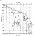
- a study on a ⁇ phase alloy plating layer formed on the brass core with respect to these technologies enables the inventor of the present invention to confirm a comparison graph of hardness and a phase diagram, the hardness being the Brinell hardness of "HYPER Zn" containing 50% by weight or more of Zn among Cu-Zn binary alloys and the phase diagram being obtained depending on a change in copper (Cu)-zinc (Zn) binary alloy phase, as illustrated in FIG. 2 , with the consultation from Korea Institute of Materials Science.
- FIG. 2 described above shows that a ⁇ phase alloy plating layer has very high Brinell hardness of 350HB or higher and very high brittleness as illustrated in FIG. 2 .
- the ⁇ phase alloy plating layer having such properties easily cracks and generates crack fragments without withstanding drawing pressure in a drawing process, and a large amount of fine debris is attached to the inside and outside of a crack. Consequently, the crack fragments and the large amount of fine debris become an impediment to improvement of a machining speed by causing secondary discharge due to the crack fragments and the fine debris when the electrical discharge machining is performed.
- the inventor again proposed a porous electrode wire for electrical discharge machining and a method for manufacturing the same disclosed in Korean Patent Registration No. 10-1284495 .
- Grains (mainly forming an ⁇ phase and a ⁇ phase) extending through the cracks formed at a second alloy layer are made of a material, of which a core is made, in a process of forming a fine line at a surface of the electrode wire for electrical discharge machining, and thereby fine debris generated due to cracking or crushing of the second alloy layer in a discharge process can be reduced by covering the second alloy layer (mainly formed by a ⁇ phase) having cracks with relatively soft grains, and a speed of the electrical discharge machining and the surface roughness of a workpiece are more improved.
- the above-described technology can improve the machining speed of the workpiece and the surface roughness of the workpiece to some extent; however, there is a limit to minimization of the fine debris of the electrode wire, the fine debris being generated when a crack (mainly second alloy layer) portion is broken.
- an electrode wire for use in electrical discharge machining and a process for preparing same disclosed in USP 5,945,010 is a patent in which a concept of crack is introduced to a wire electrode wire, similar to the patents described above.
- a core is coated with zinc having a gasification temperature lower than that of the core, through electroplating, and dispersion heat treatment process is performed for one to four hours in a temperature range of 150°C to 400°C until a galvanizing layer becomes a ⁇ phase alloy layer in order to generate a sufficient dispersion reaction between the core and the galvanizing layer coated through the electroplating, thereby manufacturing an electrode wire having pieces of ⁇ phase grains (9) formed at the surface as illustrated in FIG.3 .
- Undescribed Reference sign tf represents a maximum thickness of ⁇ phase brass alloy coating.
- the above-described technology also has an advantage in that the machining speed is improved by forming the electrode wire having the alloy plating layer formed by ⁇ phase grain pieces (9) which are an alloy of zinc and copper at a surface of the electrode wire, since the alloy plating layer having cracks at a brass core (8) is formed mainly by the ⁇ phase as illustrated in FIGS. 1 and 2 , the alloy plating layer easily cracks to generate a large amount of crack fragments and fine debris without withstanding the drawing pressure in a drawing process, and thus there is a limit to improvement of the machining speed and the surface roughness.
- the present invention is made to solve such problems described above, and an object thereof is to provide an electrode wire for electrical discharge machining which enables machining accuracy and surface roughness to be improved while enabling efficiency of discharge and a machining speed to be also improved by minimizing generation of fine debris of the electrode wire.
- Another object of the present invention is to provide an electrode wire for electrical discharge machining which exhibits a maximum cooling effect and does not generate fine debris since the electrode wire mainly has ⁇ ' phase grains, cracks, and pinholes at an outermost layer thereof and fine voids formed by ⁇ phase + ⁇ phase and a cave-shaped ⁇ phase caved in deeper than cracks from a surface toward a core of the electrode wire so as for high-pressure cooling water to infiltrate to the core.
- Still another object of the present invention is to provide an electrode wire for electrical discharge machining which has ⁇ ' phase grains and cracks at a surface of the electrode wire which are more even than ⁇ phase cracks, compared to an electrode wire in the related art which has ⁇ phase grains at a surface of the electrode wire.
- Still another object of the present invention is to provide an electrode wire for electrical discharge machining which enables a machining speed to be more improved by applying a conducting polymer to a surface of the electrode wire, thus increasing conductivity of the surface of the electrode wire.
- Still another object of the present invention is to provide an electrode wire for electrical discharge machining which enables the surface roughness and the machining accuracy to be improved by applying a polymer of semiconductor or insulator to a surface of the electrode wire or forming a semiconducting or insulating oxide layer to uniformly provide irregular discharge current and reduce even the generation of micro cracks or the like at a surface of a machined product.
- an electrode wire for electrical discharge machining including: a core made of first metal; and an alloy layer which is formed at an outer circumference of the core due to inter-dispersion of the core and second metal with which an outer surface of the core is plated.
- the alloy layer includes a portion formed by ⁇ phase + ⁇ ' phase and ⁇ ' phase grains formed at an outer circumference of the portion formed by the ⁇ phase + ⁇ ' phase.
- the alloy layer has cracks formed at a surface thereof.
- At least a part of the outer circumference of the portion formed by the ⁇ phase + ⁇ ' phase has a sunken portion, and the ⁇ ' phase grains are formed to be embedded in the sunken portion formed at the outer circumference of the portion formed by the ⁇ phase + ⁇ ' phase.
- the ⁇ ' phase grains are formed to be embedded in a wedge shape in an outer perimeter of the portion formed by the ⁇ phase + ⁇ ' phase.
- the ⁇ ' phase grains are discontinuously formed at an outer perimeter of the portion formed by the ⁇ phase + ⁇ ' phase.
- the alloy layer further contains ⁇ ' phase + ⁇ phase grains.
- the alloy layer further has pinholes formed at the surface thereof.
- the pinholes have a surface layer formed by at least one of ⁇ phase + ⁇ phase and an ⁇ phase.
- the alloy layer further has cave-shaped fine voids caved in deeper than the cracks from the surface toward the core.
- a surface layer of a portion having the cave-shaped fine voids is formed by at least one of the ⁇ phase + ⁇ phase and the ⁇ phase.
- the ⁇ ' phase grains have cracks.
- At least a part of the core penetrates the alloy layer and is exposed to a surface of the electrode wire.
- At least one of an oxide layer, a conducting polymer, a semiconducting polymer, and an insulating polymer is applied to the surface of the alloy layer.
- the first metal is made of any one of copper, brass, or metal containing copper
- the second metal is made of any one of zinc, aluminum, tin, or an alloy thereof.
- the present invention can provide an electrode wire for electrical discharge machining which enables machining accuracy and surface roughness to be improved while enabling efficiency of discharge and a machining speed to be also improved by minimizing generation of fine debris of the electrode wire.
- the present invention can provide an electrode wire for electrical discharge machining which exhibits a maximum cooling effect and does not generate fine debris, since the electrode wire mainly has ⁇ ' phase grains, cracks, and pinholes at an outermost layer thereof and a cave-shaped fine voids formed by ⁇ phase + ⁇ phase and ⁇ phase caved in deeper than cracks from a surface toward a core of the electrode wire so as for high-pressure cooling water to infiltrate to the core.
- the present invention can provide an electrode wire for electrical discharge machining which has ⁇ ' phase grains and cracks at the surface of the electrode wire which are more even than ⁇ phase cracks, compared to an electrode wire in the related art which has ⁇ phase grains at a surface of the electrode wire.
- the present invention can further improve the machining speed by applying a conducting polymer to the surface of the electrode wire and thus increasing conductivity of the surface of the electrode wire.
- the present invention can provide an electrode wire for electrical discharge machining which enables the surface roughness and the machining accuracy to be improved by applying a polymer of semiconductor or insulator to the surface of the electrode wire or forming a semiconducting or insulating oxide layer to uniformly provide irregular discharge current and reduce the generation of micro cracks or the like at a surface of a machined product.
- the present invention can obtain an effect of inhibiting re-discharge or the like due to fine debris, since a conducting polymer, a semiconducting polymer, or an insulating polymer is applied to the surface of the electrode wire such that the fine debris can be inhibited from being detached.
- the electrode wire for electrical discharge machining includes a core and an alloy layer as illustrated in a magnified photograph of a cross section in FIG. 4 .
- the core is a wire rod made of first metal which is positioned at a central portion of the electrode wire, and various types of metal can be used as the first metal which is the material of the wire rod.
- first metal which is the material of the wire rod.
- any one of copper, brass, or metal containing copper can be used, and preferably a brass core or the like containing 65% by weight of copper and 35% by weight of zinc, 63% by weight of copper and 37% by weight of zinc, or 60% by weight of copper and 40% by weight of zinc can be used.
- the core is covered with the alloy layer to be described below at an outer circumference thereof; however, at least a part of the core can penetrate the alloy layer to be described below, depending on a manufacturing process, to be exposed to the surface of the electrode wire such that components of the core can be detected at the surface of the electrode wire.
- the alloy layer is a layer formed at the outer circumference of the core due to inter-dispersion of the core and second metal coated on an outer surface of the core, and the second metal can be made of any one of zinc, aluminum, tin, or an alloy thereof which has a gasification temperature lower than that of the core, and preferably zinc can be used.
- the alloy layer has a portion formed by ⁇ phase + ⁇ ' phase illustrated in a Cu-Zn binary phase diagram in FIG. 1 and ⁇ ' phase grains formed at an outer circumference of the portion formed by the ⁇ phase + ⁇ ' phase, and an outer perimeter of the alloy layer, that is, a portion constituting the surface of the electrode wire has cracks as illustrated in the magnified photograph of the cross section in FIG. 4 .
- the cracks results in an increase in surface area of the alloy layer formed at an outer perimeter of the electrode wire to increase a contact area with cooling water, thus maximizing a cooling effect to contribute to improvement of a machining speed.
- the portion formed by the ⁇ phase + ⁇ ' phase is a portion having a composition of a zone illustrated as ⁇ + ⁇ ' in the Cu-Zn binary phase diagram in FIG. 1 and is formed at an outer perimeter of the core to cover the core, and the ⁇ ' phase grains to be described below are positioned at the outer perimeter of the portion formed by the ⁇ phase + ⁇ ' phase.
- the portion formed by the ⁇ phase + ⁇ ' phase can be formed to partially penetrate the ⁇ ' phase grains to be described below so as to reach a surface layer.
- the portion formed by the ⁇ phase + ⁇ ' phase partially forms the outermost surface layer of the alloy layer, although taking up a small portion.
- the ⁇ ' phase grains are formed to be embedded in the outer perimeter of the portion formed by the ⁇ phase + ⁇ ' phase so as to have a portion which is sunk in at least a part of the portion formed by the ⁇ phase + ⁇ ' phase as illustrated in the magnified photograph of the cross section in FIG. 4 .
- the ⁇ ' phase grains can be formed to be wedged in the outer perimeter of the portion formed by the ⁇ phase + ⁇ ' phase depending on a location, and cracks are formed on or around the ⁇ ' phase grains.
- the ⁇ ' phase grains can be discontinuously formed at the outer perimeter of the portion formed by the ⁇ phase + ⁇ ' phase or can be formed not to completely cover the outer circumference of the portion formed by the ⁇ phase + ⁇ ' phase.
- the ⁇ ' phase grains are discontinuously formed at the outer perimeter of the portion formed by the ⁇ phase + ⁇ ' phase, a part of the portion formed by the ⁇ phase + ⁇ ' phase is directly exposed to the surface of the alloy layer.
- the alloy layer can further have a portion formed by ⁇ ' phase + ⁇ phase grains illustrated in the Cu-Zn binary phase diagram in FIG. 1 .
- the surface of the alloy layer can have a mixed state of the ⁇ ' phase grains, the portion formed by the ⁇ phase + ⁇ ' phase, and the portion formed by ⁇ ' phase + ⁇ phase grains.
- the surface of alloy layer can further have pinholes or cave-shaped fine voids, as well as cracks, as illustrated in a magnified photograph of the surface in FIG. 6 and a magnified photograph of a cross section in FIG. 7 .
- the cave-shaped fine voids can be formed to be caved in deeper than the cracks from the surface toward the core of the electrode wire as illustrated in the magnified photograph of the cross section in FIG. 7 . Since a surface layer of a portion in which the cave-shaped fine voids are formed can be partially gasified in manufacturing processes such as a dispersion heat treatment or drawing to be subjected to a dezincification phenomenon, a zinc concentration is increased such that ⁇ phase + ⁇ phase or an ⁇ phase illustrated in FIGS. 1 and 2 can be found, and the ⁇ phase + ⁇ phase and the ⁇ phase can be found to be mixed depending on a location.
- FIG. 8 illustrates a state where a surface layer of the cave-shaped fine voids has the ⁇ phase + ⁇ phase as 23.6% of Cu and 76.37% of Zn.
- the cave-shaped fine voids enable high-pressure cooling water provided during the electrical discharge machining to infiltrate even to a core region (in a case of the cave-shaped fine voids extending to the core region), thus significantly improving a cooling effect.
- a zinc component having the ⁇ phase and the ⁇ phase + ⁇ phase, by which the surface layer of the cave-shaped fine voids is formed are easily gasified to take away heat, thus further improving the cooling effect to significantly improve a speed of the electrical discharge machining.
- FIG. 9 illustrates a state where a surface layer of the pinholes formed at the surface of the alloy layer has phases as 13.90% of Cu and 86.10% of Zn.
- the electrode wire for electrical discharge machining includes the portion formed by ⁇ phase + ⁇ ' phase which is formed around the core and the ⁇ ' phase grains embedded in the outer perimeter of the portion formed by the ⁇ phase + ⁇ ' phase, and cracks are formed on or around the ⁇ ' phase grains.
- a ⁇ phase alloy layer is a brittle alloy layer by having the hardness of 350HB or higher as illustrated in FIG. 2 .
- the ⁇ ' phase grains of the present invention cause the surface layer of the electrode wire to have a much lower hardness as illustrated in FIG. 2 than the hardness of the ⁇ phase alloy layer in the related art and the surface layer is flexible, the surface layer does not crack in the drawing process, thus allowing little fine debris to be attached to the surface of the electrode wire.
- secondary discharge due to the fine debris is reduced during the electrical discharge machining such that the machining speed and the surface roughness are not only significantly improved, but also diamond guide dies through which the electrode wire passes can be inhibited from being clogged or the like.
- a machining speed of an electrode wire having the ⁇ phase is generally known to be faster than a machining speed of an electrode wire having the ⁇ ' phase.
- the surface of the alloy layer of the electrode wire of the present invention is mostly formed by the ⁇ ' phase grains having a higher copper concentration and a lower zinc concentration than those of the ⁇ phase which is known to be fastest in the related art, little fine debris is attached to the surface of the alloy layer of the present invention, the surface has the ⁇ ' phase grains and numerous cracks and numerous pinholes formed around the ⁇ ' phase grains, and cave-shaped fine voids formed by the ⁇ phase + ⁇ phase or the ⁇ phase are formed to extend to a portion deeper than the cracks or the pinholes.
- the surface has multiple elements that remarkably improve the cooling effect by causing high-pressure cooling water to infiltrate to the core, and thus the machining speed turns out to be improved to at least 108% or more than the machining speed of the electrode wire having cracks on the ⁇ phase in the related art.
- a method for manufacturing an electrode wire for electrical discharge machining according to the preferred embodiment of the present invention having such a structure described above is described as follows.
- the method for manufacturing an electrode wire for electrical discharge machining is related to a method for manufacturing the electrode wire described above, and a specific embodiment includes a core providing step, a plating step, a primary dispersion heat treatment performing step, a primary drawing step, a secondary dispersion heat treatment performing step, and a secondary drawing step.
- the manufacturing method can be performed by variously selecting and modifying a dispersion heat treatment method, a temperature and a time of the dispersion heat treatment, a process of a plating method or the like in various manners suitable for equipment possessed by a company within a range not departing from a basic concept of the present invention.
- Table 1 to be provided below shows machining test results of machined products obtained by using the electrode wire having a wire diameter of ⁇ 0.25 mm according to the present invention manufactured as described above and electrode wires according to Comparative Examples 1 and 2.
- Present Invention Comparative Example 1 Comparative Example 2 1st Cut 787 sec 108% 848 sec 100% 835 sec 102% 2nd Cut 177 sec 114% 201 sec 100% 202 sec 100% Total 964 sec 109% 1,049 sec 100% 1,037 sec 101%
- the machining test example shown in Table 1 was processed by Charmilles Robofil 240SL in accordance with ST25A. Tec.
- Comparative Example 1 is Thermo JP2 manufactured by THERMOCOMPACT in France and is an electrode wire having a wire diameter of ⁇ 0.25 mm which has cracks at a surface of a ⁇ phase alloy layer thereof
- Comparative Example 2 is Topas PLUS H manufactured by Berkenhoff H in Germany and is an electrode wire having a wire diameter of ⁇ 0.25 mm which has cracks at a surface of a ⁇ phase alloy layer thereof.
- the electrode wire of the present invention improves the machining speed to at least 108% or higher in the primary machining and to a maximum of 114% in the secondary machining.
- the alloy layer of the electrode wire is described to contain the portion formed by the ⁇ phase + ⁇ ' phase and the ⁇ ' phase grains formed at the outer circumference of the portion formed by the ⁇ phase + ⁇ ' phase in the example described above; however, the surface of the alloy layer can be manufactured to have the ⁇ ' phase grains at most thereof and a mixed state of the ⁇ phase grains or the ⁇ phase + ⁇ phase grains at some parts thereof by changing some of dispersion heat treatment conditions, the drawing process, and the like.
- Most of the surface of the alloy layer of the electrode wire manufactured as described above is formed by the ⁇ ' phase grains, and some parts thereof include both the portion formed by the ⁇ phase + ⁇ ' phase and a portion formed by the ⁇ phase grains or the ⁇ phase + ⁇ phase grains.
- the electrode wire according to the present invention can have an oxide layer on the surface layer of the portion which is exposed to the surface of the electrode wire and portions which form cracks, pinholes, and cave-shaped fine voids of the portion formed by the ⁇ ' phase grains and the ⁇ phase + ⁇ ' phase.
- the oxide layer increases absorption of the cooling water and conductance to improve discharge power, and thus the machining speed can be further improved.
- the electrode wire according to the present invention can increase the conductance of the surface of the electrode wire by applying a conducting polymer to the surface of the electrode wire and can improve the machining speed by inhibiting the generation of fine debris.
- the conducting polymer has very good conductivity of 100 s/cm or higher as illustrated in property values of the conductivity of FIG. 11 , and examples thereof can include doped PEDOT, doped polyaniline, and the like.
- FIG. 12 illustrates an example of corrosion preventive experiment of metal by using doped polyaniline
- (A) of FIG. 12 illustrates a surface state of an iron plate
- (B) of FIG. 12 illustrates a photograph taken after a chlorine spray test for testing corrosion resistance by spraying a 0.5 M NaCl solution to promote corrosion, after polyaniline is applied to a surface of the iron plate illustrated in (A) of FIG. 9 .
- the photograph in (B) of FIG. 12 can clearly show that a portion coated with polyaniline is not corroded at all and an uncoated portion is considerably corroded.
- a semiconducting polymer or an insulating polymer can be applied to the surface of the alloy layer of the electrode wire according to the present invention.
- the semiconducting polymer and the insulating polymer stabilize an amplitude of the discharge current to a normal state, thus stabilizing a discharge pulse height, a pulse width, a rise time, a fall time, or the like such that the surface roughness and the machining accuracy of the machined product are further improved.
- At least one of an oxide layer, a conducting polymer, a semiconducting polymer, and an insulating polymer can be applied to the surface of the alloy layer; however, one or more thereof can be applied to the surface.
- a configuration of a technology of the electrode wire for electrical discharge machining of the present invention described above is not limited to the contents of the detailed description of the invention and can be variously modified within a range without departing from the technical idea and objects of the present invention.
- the present invention is applicable to an electrode wire for electrical discharge machining which minimizes the generation of fine debris during the electrical discharge machining, and thus re-discharge does not occur such that a machining speed is improved and the surface roughness of a workpiece is significantly improved.
Landscapes
- Chemical & Material Sciences (AREA)
- Engineering & Computer Science (AREA)
- Mechanical Engineering (AREA)
- Chemical Kinetics & Catalysis (AREA)
- Materials Engineering (AREA)
- Metallurgy (AREA)
- Organic Chemistry (AREA)
- Inorganic Chemistry (AREA)
- Manufacturing & Machinery (AREA)
- Electrochemistry (AREA)
- Electrical Discharge Machining, Electrochemical Machining, And Combined Machining (AREA)
- Electroplating Methods And Accessories (AREA)
Applications Claiming Priority (2)
| Application Number | Priority Date | Filing Date | Title |
|---|---|---|---|
| KR1020190120972A KR102774367B1 (ko) | 2019-09-30 | 2019-09-30 | 방전가공용 전극선 |
| PCT/KR2020/013251 WO2021066471A1 (ko) | 2019-09-30 | 2020-09-28 | 방전가공용 전극선 |
Publications (2)
| Publication Number | Publication Date |
|---|---|
| EP4043135A1 true EP4043135A1 (de) | 2022-08-17 |
| EP4043135A4 EP4043135A4 (de) | 2023-12-06 |
Family
ID=75338326
Family Applications (1)
| Application Number | Title | Priority Date | Filing Date |
|---|---|---|---|
| EP20871898.1A Pending EP4043135A4 (de) | 2019-09-30 | 2020-09-28 | Elektrodendraht für eine elektroerosivbearbeitung |
Country Status (6)
| Country | Link |
|---|---|
| US (1) | US20220339724A1 (de) |
| EP (1) | EP4043135A4 (de) |
| JP (1) | JP7698319B2 (de) |
| KR (1) | KR102774367B1 (de) |
| CN (1) | CN114423556B (de) |
| WO (1) | WO2021066471A1 (de) |
Family Cites Families (21)
| Publication number | Priority date | Publication date | Assignee | Title |
|---|---|---|---|---|
| JPS58165927A (ja) * | 1982-03-25 | 1983-10-01 | Inoue Japax Res Inc | ワイヤカツト放電加工用電極線 |
| US4686153A (en) | 1984-12-08 | 1987-08-11 | Fujikura Ltd. | Electrode wire for use in electric discharge machining and process for preparing same |
| CN1078831C (zh) * | 1997-07-30 | 2002-02-06 | 成机哲 | 放电加工用多孔性电极线及其制造方法 |
| US5945010A (en) | 1997-09-02 | 1999-08-31 | Composite Concepts Company, Inc. | Electrode wire for use in electric discharge machining and process for preparing same |
| JPH11347847A (ja) * | 1998-06-10 | 1999-12-21 | Oki Electric Cable Co Ltd | ワイヤ放電加工用電極線 |
| JP2001322035A (ja) | 2000-05-18 | 2001-11-20 | Oki Electric Cable Co Ltd | ワイヤカット放電加工用電極線 |
| JP2003039246A (ja) * | 2001-07-27 | 2003-02-12 | Oki Electric Cable Co Ltd | ワイヤ放電加工用電極線 |
| FR2833875B1 (fr) * | 2001-12-21 | 2004-07-02 | Thermocompact Sa | Fil pour electroerosion a grande vitesse d'usinage |
| JP4390581B2 (ja) * | 2004-02-16 | 2009-12-24 | サンエツ金属株式会社 | ワイヤ放電加工用電極線 |
| JP2005254408A (ja) | 2004-03-12 | 2005-09-22 | Sumitomo Electric Ind Ltd | ワイヤ放電加工用電極線およびその製造方法 |
| KR100632149B1 (ko) * | 2005-09-23 | 2006-10-11 | 홍덕스틸코드주식회사 | 와이어 방전 가공용 전극선 |
| JP4931028B2 (ja) * | 2010-02-02 | 2012-05-16 | 沖電線株式会社 | ワイヤ放電加工用電極線、その製造方法及びその電極線を用いた放電加工方法 |
| KR101284495B1 (ko) | 2011-04-29 | 2013-07-16 | 성기철 | 방전가공용 전극선 및 그 제조방법 |
| WO2013037336A1 (de) * | 2011-09-16 | 2013-03-21 | Heinrich Stamm Gmbh | Drahtelektrode zum funkenerosiven schneiden von gegenständen |
| EP2872261B1 (de) * | 2012-07-12 | 2016-09-14 | Tata Steel UK Limited | Mikrowellenhärtung mehrschichtiger beschichtungen |
| KR20140051734A (ko) | 2012-10-23 | 2014-05-02 | 성기철 | 방전가공용 전극선 및 그 제조방법 |
| KR20140100796A (ko) * | 2013-02-07 | 2014-08-18 | 성기철 | 방전가공용 전극선 및 그 제조방법 |
| DE102017008325B4 (de) | 2017-08-29 | 2021-10-28 | Berkenhoff Gmbh | Drahtelektrode zum funkenerosiven Schneiden eines Gegenstandes |
| FR3083466B1 (fr) | 2018-07-03 | 2020-12-18 | Thermocompact Sa | Fil electrode a couche poreuse pour electroerosion |
| MX2021013202A (es) * | 2019-05-10 | 2022-03-11 | Berkenhoff Gmbh | Electrodo de alambre para corte por electroerosion y metodo para producir este electrodo de alambre. |
| JP7823534B2 (ja) * | 2022-09-22 | 2026-03-04 | 株式会社プロテリアル | ワイヤー放電加工用電極線 |
-
2019
- 2019-09-30 KR KR1020190120972A patent/KR102774367B1/ko active Active
-
2020
- 2020-09-28 EP EP20871898.1A patent/EP4043135A4/de active Pending
- 2020-09-28 JP JP2022517468A patent/JP7698319B2/ja active Active
- 2020-09-28 WO PCT/KR2020/013251 patent/WO2021066471A1/ko not_active Ceased
- 2020-09-28 CN CN202080068276.7A patent/CN114423556B/zh active Active
- 2020-09-28 US US17/765,174 patent/US20220339724A1/en active Pending
Also Published As
| Publication number | Publication date |
|---|---|
| WO2021066471A1 (ko) | 2021-04-08 |
| US20220339724A1 (en) | 2022-10-27 |
| KR20210038172A (ko) | 2021-04-07 |
| CN114423556B (zh) | 2025-05-30 |
| JP7698319B2 (ja) | 2025-06-25 |
| JP2022550014A (ja) | 2022-11-30 |
| KR102774367B1 (ko) | 2025-03-21 |
| EP4043135A4 (de) | 2023-12-06 |
| CN114423556A (zh) | 2022-04-29 |
Similar Documents
| Publication | Publication Date | Title |
|---|---|---|
| US5945010A (en) | Electrode wire for use in electric discharge machining and process for preparing same | |
| RU2516125C2 (ru) | Проволочный электрод для электроэрозионной резки | |
| JP3718529B2 (ja) | 放電加工用多孔性電極線の製造方法 | |
| KR101292343B1 (ko) | 방전가공용 전극선 및 그 제조방법 | |
| EP2005343B1 (de) | Edm-leitung | |
| KR100543847B1 (ko) | 방전가공용 전극선 및 그 제조 방법 | |
| JP7581240B2 (ja) | スパーク浸食切断のためのワイヤ電極および該ワイヤ電極を生産する方法 | |
| JP7314185B2 (ja) | 放電加工用の多孔質層を有する電極リード | |
| TW200918220A (en) | Electrode wire for spark erosion | |
| US20060138091A1 (en) | Method of manufacturing zinc-coated electrode wire for electric discharge processors using hot dip galvanizing process | |
| EP4043135A1 (de) | Elektrodendraht für eine elektroerosivbearbeitung | |
| KR100925000B1 (ko) | 방전가공용 전극선 및 그 제조방법 | |
| US20070295695A1 (en) | EDM wire | |
| KR102629017B1 (ko) | 고성능 액체 크로마토그래피용 컬럼의 제조방법 | |
| RU2810276C2 (ru) | Проволочный электрод для электроэрозионной резки и способ получения такого проволочного электрода | |
| Hamdi | Ibrahem Maher, Ahmed AD Sarhan & | |
| KR20130030797A (ko) | 방전가공용 전극선 및 그 제조방법 | |
| KR20200049183A (ko) | 방전가공용 전극선 및 그 제조방법 | |
| KR20140075442A (ko) | 방전가공용 전극선 및 그 제조방법 | |
| CA2556000A1 (en) | Edm wire |
Legal Events
| Date | Code | Title | Description |
|---|---|---|---|
| STAA | Information on the status of an ep patent application or granted ep patent |
Free format text: STATUS: THE INTERNATIONAL PUBLICATION HAS BEEN MADE |
|
| PUAI | Public reference made under article 153(3) epc to a published international application that has entered the european phase |
Free format text: ORIGINAL CODE: 0009012 |
|
| STAA | Information on the status of an ep patent application or granted ep patent |
Free format text: STATUS: REQUEST FOR EXAMINATION WAS MADE |
|
| 17P | Request for examination filed |
Effective date: 20220428 |
|
| AK | Designated contracting states |
Kind code of ref document: A1 Designated state(s): AL AT BE BG CH CY CZ DE DK EE ES FI FR GB GR HR HU IE IS IT LI LT LU LV MC MK MT NL NO PL PT RO RS SE SI SK SM TR |
|
| DAV | Request for validation of the european patent (deleted) | ||
| DAX | Request for extension of the european patent (deleted) | ||
| A4 | Supplementary search report drawn up and despatched |
Effective date: 20231107 |
|
| RIC1 | Information provided on ipc code assigned before grant |
Ipc: B23H 7/08 20060101ALI20231031BHEP Ipc: B23H 1/06 20060101AFI20231031BHEP |