EP4043264B1 - Treiberschaltung - Google Patents
Treiberschaltung Download PDFInfo
- Publication number
- EP4043264B1 EP4043264B1 EP21814463.2A EP21814463A EP4043264B1 EP 4043264 B1 EP4043264 B1 EP 4043264B1 EP 21814463 A EP21814463 A EP 21814463A EP 4043264 B1 EP4043264 B1 EP 4043264B1
- Authority
- EP
- European Patent Office
- Prior art keywords
- module
- signal
- level
- delay
- side driver
- Prior art date
- Legal status (The legal status is an assumption and is not a legal conclusion. Google has not performed a legal analysis and makes no representation as to the accuracy of the status listed.)
- Active
Links
Images




Classifications
-
- G—PHYSICS
- G05—CONTROLLING; REGULATING
- G05B—CONTROL OR REGULATING SYSTEMS IN GENERAL; FUNCTIONAL ELEMENTS OF SUCH SYSTEMS; MONITORING OR TESTING ARRANGEMENTS FOR SUCH SYSTEMS OR ELEMENTS
- G05B19/00—Program-control systems
- G05B19/02—Program-control systems electric
- G05B19/04—Program control other than numerical control, i.e. in sequence controllers or logic controllers
- G05B19/05—Programmable logic controllers, e.g. simulating logic interconnections of signals according to ladder diagrams or function charts
- G05B19/056—Programming the PLC
-
- B—PERFORMING OPERATIONS; TRANSPORTING
- B60—VEHICLES IN GENERAL
- B60L—PROPULSION OF ELECTRICALLY-PROPELLED VEHICLES; SUPPLYING ELECTRIC POWER FOR AUXILIARY EQUIPMENT OF ELECTRICALLY-PROPELLED VEHICLES; ELECTRODYNAMIC BRAKE SYSTEMS FOR VEHICLES IN GENERAL; MAGNETIC SUSPENSION OR LEVITATION FOR VEHICLES; MONITORING OPERATING VARIABLES OF ELECTRICALLY-PROPELLED VEHICLES; ELECTRIC SAFETY DEVICES FOR ELECTRICALLY-PROPELLED VEHICLES
- B60L3/00—Electric devices on electrically-propelled vehicles for safety purposes; Monitoring operating variables, e.g. speed, deceleration or energy consumption
- B60L3/0023—Detecting, eliminating, remedying or compensating for drive train abnormalities, e.g. failures within the drive train
-
- B—PERFORMING OPERATIONS; TRANSPORTING
- B60—VEHICLES IN GENERAL
- B60L—PROPULSION OF ELECTRICALLY-PROPELLED VEHICLES; SUPPLYING ELECTRIC POWER FOR AUXILIARY EQUIPMENT OF ELECTRICALLY-PROPELLED VEHICLES; ELECTRODYNAMIC BRAKE SYSTEMS FOR VEHICLES IN GENERAL; MAGNETIC SUSPENSION OR LEVITATION FOR VEHICLES; MONITORING OPERATING VARIABLES OF ELECTRICALLY-PROPELLED VEHICLES; ELECTRIC SAFETY DEVICES FOR ELECTRICALLY-PROPELLED VEHICLES
- B60L3/00—Electric devices on electrically-propelled vehicles for safety purposes; Monitoring operating variables, e.g. speed, deceleration or energy consumption
- B60L3/0023—Detecting, eliminating, remedying or compensating for drive train abnormalities, e.g. failures within the drive train
- B60L3/0084—Detecting, eliminating, remedying or compensating for drive train abnormalities, e.g. failures within the drive train relating to control modules
-
- B—PERFORMING OPERATIONS; TRANSPORTING
- B60—VEHICLES IN GENERAL
- B60L—PROPULSION OF ELECTRICALLY-PROPELLED VEHICLES; SUPPLYING ELECTRIC POWER FOR AUXILIARY EQUIPMENT OF ELECTRICALLY-PROPELLED VEHICLES; ELECTRODYNAMIC BRAKE SYSTEMS FOR VEHICLES IN GENERAL; MAGNETIC SUSPENSION OR LEVITATION FOR VEHICLES; MONITORING OPERATING VARIABLES OF ELECTRICALLY-PROPELLED VEHICLES; ELECTRIC SAFETY DEVICES FOR ELECTRICALLY-PROPELLED VEHICLES
- B60L58/00—Methods or circuit arrangements for monitoring or controlling batteries or fuel cells, specially adapted for electric vehicles
- B60L58/10—Methods or circuit arrangements for monitoring or controlling batteries or fuel cells, specially adapted for electric vehicles for monitoring or controlling batteries
-
- H—ELECTRICITY
- H03—ELECTRONIC CIRCUITRY
- H03K—PULSE TECHNIQUE
- H03K17/00—Electronic switching or gating, i.e. not by contact-making and –breaking
- H03K17/10—Modifications for increasing the maximum permissible switched voltage
-
- H—ELECTRICITY
- H03—ELECTRONIC CIRCUITRY
- H03K—PULSE TECHNIQUE
- H03K17/00—Electronic switching or gating, i.e. not by contact-making and –breaking
- H03K17/28—Modifications for introducing a time delay before switching
-
- H—ELECTRICITY
- H01—ELECTRIC ELEMENTS
- H01H—ELECTRIC SWITCHES; RELAYS; SELECTORS; EMERGENCY PROTECTIVE DEVICES
- H01H47/00—Circuit arrangements not adapted to a particular application of the relay and designed to obtain desired operating characteristics or to provide energising current
- H01H47/002—Monitoring or fail-safe circuits
-
- H—ELECTRICITY
- H01—ELECTRIC ELEMENTS
- H01H—ELECTRIC SWITCHES; RELAYS; SELECTORS; EMERGENCY PROTECTIVE DEVICES
- H01H47/00—Circuit arrangements not adapted to a particular application of the relay and designed to obtain desired operating characteristics or to provide energising current
- H01H47/22—Circuit arrangements not adapted to a particular application of the relay and designed to obtain desired operating characteristics or to provide energising current for supplying energising current for relay coil
- H01H47/32—Energising current supplied by semiconductor device
-
- H—ELECTRICITY
- H03—ELECTRONIC CIRCUITRY
- H03K—PULSE TECHNIQUE
- H03K2217/00—Indexing scheme related to electronic switching or gating, i.e. not by contact-making or -breaking covered by H03K17/00
- H03K2217/0063—High side switches, i.e. the higher potential [DC] or life wire [AC] being directly connected to the switch and not via the load
Definitions
- Embodiments of this application relate to the field of electricity, and in particular, to a drive circuit.
- a second embodiment in the embodiments of this application relates to a drive circuit.
- This embodiment is approximately the same as the first embodiment, with a main difference as follows:
- An example in which the drive circuit is configured to drive a load is used to describe a connection manner of the drive circuit and the load, and a function of the drive circuit.
- the preset duration of the control module 203 ranges approximately from 1 second (s) to 3 seconds
- the preset duration is greater than 3 seconds.
- the high-side driver module 201 is configured to: according to the delay signal of preset duration, remain in a first state within the preset duration, where the first state is the same as a second state.
- the second state is a working state of the high-side driver module 201 before the control module 203 is reset, and the second state includes being on or off.
- the high-side driver module 201 is configured to perform switching-on or switching-off according to the drive signal from the control module 203.
- the load 101 in this embodiment may be a device such as a relay or a contactor, or may be another device such as a pump (PUMP) or a valve. Details are not listed herein.
- the load 101 is the relay and the control module 203 is a microcontroller in a battery management system of a vehicle is used below to describe the drive circuit mentioned in this embodiment.
- a relay is usually used as a switch for connection or disconnection. Switching on and off of the relay are usually controlled by the microcontroller of the battery management system.
- the microcontroller may be reset during driving, and the reset duration is relatively short. When the microcontroller is being reset, no drive signal can be output. In this case, the relay abruptly switches off and the vehicle abruptly stops, causing a great safety hazard. In addition, disconnecting the relay with the load has great impact on service life of the relay.
- a delay module 202 is added between the high-side driver module 201 and the microcontroller.
- the delay signal output by the delay module 202 to the high-side driver module 201 can keep the relay in an on state, so that the relay is not accidentally switched off.
- the delay signal output by the delay module 202 to the high-side driver module 201 can keep the relay off, so that the relay is not accidentally switched on.
- the vehicle field is used as an example to describe the drive circuit.
- the drive circuit may also be applied to another field.
- the application field of the drive circuit is not limited in this embodiment.
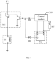
- the delay module 202 includes a delay unit and a first pull-up unit; a first controlled terminal of the delay unit is connected to both the first pull-up unit and a first output terminal of the control module 203, a second controlled terminal of the delay unit is connected to a second output terminal of the control module 203, and an output terminal of the delay unit is connected to a control terminal of the high-side driver module 201.
- the first pull-up unit pulls up an input signal of the first controlled terminal of the delay unit to a high level signal.
- the delay unit is configured to: when an electrical signal of a first level is detected at the first controlled terminal and an edge signal is detected at the second controlled terminal, output a delay signal of a second level to a high-side driver unit, to control the high-side driver module 201 to switch on; when an electrical signal of a first level is detected at the first controlled terminal and no edge signal is detected at the second controlled terminal, output a delay signal of a fourth level to a high-side driver module 201, to control the high-side driver module 201 to switch off; and when an electrical signal of a third level is detected at the first controlled terminal, output a delay signal of a fourth level to a high-side driver module 201, to control the high-side driver module 201 to switch off.
- the fourth level is a reverse level of the second level
- the third level is a reverse level of the first level
- the high-side driver module 201 remains on when receiving an electrical signal of the second level and switched off when receiving an electrical signal of the fourth level.
- the edge signal may be a rising edge signal or a falling edge signal.
- a person skilled in the art can determine a circuit form of the delay unit based on working logic of the delay unit.
- the delay module 202 further includes a second pull-up unit, and the second pull-up unit is connected to the second controlled terminal of the delay unit.
- the first level and the second level are co-directional levels
- the third level and the fourth level are co-directional levels
- the first level and the third level are reverse levels. It is assumed that the first level and the second level are high levels
- the third level and the fourth level are low levels
- a high-level delay signal output by the delay unit when a high-level electrical signal is detected at the first controlled terminal and an edge signal is detected at the second controlled terminal is a pulse signal, that is, a high-level pulse signal.
- input and output level states that can be implemented by the delay unit are shown in Table 1.
- Table 1 First controlled terminal Second controlled terminal Output terminal Case 1 Low level Any level Low level Case 2 High level Edge signal High-level pulse
- a delay time (namely, the preset duration) of the delay unit can be set based on a reset time of the control module 203, so that the preset duration is greater than reset duration of the control module 203.
- a resistance value, a capacitance value, and the like of a corresponding circuit device are selected based on the delay time of the delay unit.
- a specific circuit form of the delay unit is not limited in this embodiment.
- either of the first pull-up unit and the second pull-up unit includes a pull-up resistor, a first terminal of the pull-up resistor is connected to a signal terminal of a pull-up power supply, and a second terminal of the pull-up resistor serves as an output terminal of the pull-up unit.
- first pull-up unit and the second pull-up unit may also use another circuit structure.
- This embodiment is only used as an example for illustration, and imposes no limitation on specific circuits of the first pull-up unit and the second pull-up unit.
- a structure of the first pull-up unit may be the same as or different from a structure of the second pull-up unit.
- This embodiment is illustrated using an example that they are the same, but imposes no limitation on a circuit structure in actual use.
- the signal terminal of the pull-up power supply may be an output terminal of the pull-up power supply, and a voltage output by the pull-up power supply may be the same as a high-level voltage of a signal output by the control module 203.
- a voltage value of the pull-up power supply is not limited in this embodiment. The following uses an example in which the edge signal is the falling edge with reference to different forms of drive circuits and protective circuits to illustrate a working principle of the drive circuit.
- a delay unit includes a delay component.
- a first input terminal of the delay component is the first controlled terminal of the delay unit, a second input terminal of the delay component serves as the second controlled terminal of the delay unit, and an output terminal of the delay component serves as the output terminal of the delay unit.
- the delay component is configured to generate a delay signal of a corresponding level based on an electrical signal received by the first input terminal of the delay component and the electrical signal received by the second input terminal of the delay component, to control the high-side driver module 201 to switch off or on.
- Table 1 For a level relationship between the electrical signal received by the first input terminal of the delay component, the electrical signal received by the second input terminal of the delay component, and the output delay signal, refer to descriptions in Table 1.
- the control module 203 Because the control module 203 outputs the drive signal of the second level to the high-side driver module 201, the high-side driver module 201 is on regardless of whether the delay module 202 outputs the electrical signal of the second level or the electrical signal of the fourth level.
- the control module 203 is being reset, the first controlled terminal of the delay unit is pulled up to the first level, and the second controlled terminal of the delay unit can detect the edge signal, to output a delay signal of the second level to the high-side driver module 201, so that the high-side driver module 201 remains on.
- the control module 203 After detecting a switch-off signal, the control module 203 outputs the drive signal of the fourth level to the high-side driver module 201, and outputs the control signal of the third level to the first controlled terminal of the delay module 202 and the second controlled terminal of the delay module 202. Because the control module 203 outputs the drive signal of the fourth level to the high-side driver module 201 and the delay module 202 outputs the delay signal of the fourth level to the high-side driver module 201, the high-side driver module 201 is off.
- the delay module 202 When the control module 203 is being reset, the first controlled terminal of the delay unit is pulled up to the first level, and the second controlled terminal of the delay unit cannot detect a specific edge signal, and therefore, the delay module 202 outputs the delay signal of the fourth level to the high-side driver module 201, so that the high-side driver module 201 remains off.
- a period of the first pulse width modulation PWM control signal is less than the preset duration; and when the edge signal is a rising edge signal, the fifth level is a low level, or when the edge signal is a falling edge signal, the fifth level is a high level.
- a device compatible with a large current may be selected as a device in the high-side driver unit, to prevent the device in the high-side driver unit from being damaged by a large current generated by a tributary circuit in which the high-side driver unit is located.
- the following uses an example to describe detection of a switch-on signal and a switch-off signal.
- the switch-on signal is a high-level signal
- the switch-off signal is a low-level signal.
- a control loop may be disposed.
- the control loop includes a control power supply, a switch (such as a single-pole switch, a push-button switch, an electronic switch, or the like), and a resistor that are connected in series in sequence. A current in the resistor is detected through a voltage detection circuit, and a detection result is output to the control module 203.
- the voltage detection circuit detects a voltage value, and then a high-level signal is output to the control module 203.
- the control module 203 receives the high-level signal, that is, detects a high-level signal, and then controls the load 101 to switch on according to the foregoing logic.
- the voltage detection circuit detects no voltage value, and then a low-level signal is output to the control module 203.
- the control module 203 receives a low-level signal, that is, detects the low-level signal, and then controls the load 101 to switch off according to the foregoing logic.
- the switch-on signal may alternatively be a switch-on command input by a staff member
- the switch-off signal may alternatively be an input switch-off command.
- the control module 203 is connected to an input device, and the control module 203 detects a command input by the staff member through the input device. After detecting the switch-on command, the control module 203 controls the load 101 to switch on based on the foregoing logic. After detecting the switch-off command, the control module 203 controls the load 101 to switch off based on the foregoing logic. Manners of generating the switch-on signal and the switch-off signal are not limited in this embodiment.
- the control module 203 after detecting the switch-on signal, the control module 203 outputs the first level to the first controlled terminal of the delay module 202, to ensure that when the control module 203 is being reset, the delay module 202 outputs a delay signal of the second level when an edge signal is detected at the second controlled terminal, so that a high-voltage driver module remains on.
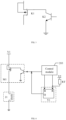
- the load 101 is a relay, because the high-side driver unit is connected to the drive power supply, a type-P transistor that has a source electrode suitable to be connected to a high level and a drain electrode suitable to be grounded through the load 101 can be selected.
- a high-level signal is generally used as an enabling signal, that is, if the high-side driver unit receives a high level, the high-side driver unit is switched on; and if the high-side driver unit receives a low level, the high-side driver unit is switched off.
- a gate of the type-P transistor may be connected to a collector of a type-NPN transistor, and an emitter of the type-NPN transistor is grounded, and a base serves as a control terminal of the entire high-side driver unit.
- the control terminal of the high-side driver unit inputs a low level
- the type-NPN transistor is not switched on
- the gate of the type-P transistor is in a high-impedance state
- the type-P transistor is not switched on, and therefore the high-side driver unit is conductive.
- the type-NPN transistor When the control terminal of the high-side driver unit inputs a high level, the type-NPN transistor is switched on, the gate of the type-P transistor is connected to a low level, the type-P transistor is switched on, and therefore the high-side driver unit is switched on.
- a circuit structure of the high-side driver unit may also be adjusted based on the change of the switching-on condition of the high-side driver unit.
- the high-side driver unit includes a type-P transistor (K1) and a type-NPN transistor (K2).
- a first terminal of the type-P transistor K1 serves as a first terminal of the high-side driver unit
- a second terminal of the type-P transistor K1 serves as a second terminal of the high-side driver unit
- a control terminal of the type-P transistor K1 is connected to a first terminal of the type-NPN transistor
- a second terminal of the type-NPN transistor K2 is grounded
- a control terminal of the type-NPN transistor K2 serves as the control terminal of the high-side driver unit.
- a level of the control signal (referred to as a control signal 1) output by the control module 203 to the first controlled terminal of the delay unit may be set based on a working principle of the delay unit, and the control signal (referred to as a control signal 2) output by the control module 203 to the second controlled terminal of the delay unit may be a constant-level signal (including a low-level signal and a high-level signal) or a pulse width modulation signal.
- the working principle of the drive circuit is as follows:
- the control module 203 When receiving a relay switch-on signal, the control module 203 outputs a high-level drive signal to the control terminal of the high-side driver unit, outputs a high-level control signal 2 to the port B of the delay component, and outputs a high-level control signal 1 to the port R of the delay component.
- a state of the port Q is a low level, and the high-side driver unit is switched on.
- the control module 203 is being reset, output of the control module 203 is in a high-impedance state, the port B of the delay component changes from a high level to a low level, and a falling edge occurs.
- the control module 203 When receiving a relay switch-off signal, the control module 203 outputs a low-level drive signal to the control terminal of the high-side driver unit, outputs a low-level control signal 1 to the port R of the delay component, and outputs a low-level control signal 2 to the port B of the delay component (a low-level control signal 1 may alternatively be first output, and then a low-level drive signal is output to the control terminal of the high-side driver unit).
- a state of the port Q is a low level, and the high-side driver unit is switched off.
- the output of the control module 203 is in a high-impedance state, and the port B of the delay component is still at a low level (no falling edge). Because of presence of the first pull-up unit, input of the port R changes from a low level to a high level, output of the port Q is still at a low level, the state of the high-side driver unit does not change, and the relay is not accidentally switched on.
- an output sequence of the control signal 1 and the drive signal may not be limited. If the interval between the control signal 1 and the drive signal is very long and greater than the action time of the relay, in this example, the low-level control signal 1 and control signal 2 are output firstly, and then the low-level drive signal is output.
- the low-level control signal 1 is output before the low-level drive signal is output, thereby preventing the relay from being switched on and then being switched off caused by resetting of the microcontroller when the low-level control signal 1 is not sent after the low-level drive signal has been sent.
- an output sequence of the control signal 1 and the control signal 2 may be set as required.
- the control signal 1 is output before the control signal 2 is output, the low-level control signal 1 can cause the delay unit to immediately output a low level, so that the relay can be immediately switched off; and when the control signal 2 is output before the control signal 1, because the first controlled terminal receives the signal later, the relay is switched off after a period of delay time.
- a time length is a time difference between a time of outputting the control signal 2 and a time of outputting the control signal 1.
- a person skilled in the art can determine the output sequence of the control signal 1 and the control signal 2 based on a requirement of a project on a response speed of a circuit in which the relay is located.
- the working principle of the drive circuit is as follows:
- the control module 203 When receiving a relay switch-on signal, the control module 203 outputs a high-level drive signal to the control terminal of the high-side driver unit, outputs a high-level control signal 1 to the port R of the delay component, and outputs a PWM control signal 2 to the port B of the delay component, so that the high-side driver unit is switched on.
- a high-level pulse is output at the port Q, which may be repeatedly triggered.
- the delay time of the delay unit is greater than a PWM period, a high level is continuously output at the port Q.
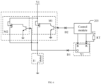
- control module 203 may be configured to: after detecting a switch-on signal, output the drive signal of the second level or a second pulse width modulation PWM control signal to the first high-side driver unit, output a control signal of the first level or the third level to the first controlled terminal of the delay module 202, and output a control signal of a fifth level or a third pulse width modulation PWM control signal to the second controlled terminal of the delay module 202; and after detecting a switch-off signal, output the drive signal of the fourth level to the first high-side driver unit, and output a control signal of the third level to the first controlled terminal and the second controlled terminal of the delay module 202, where a period of the third pulse width modulation PWM control signal is less than the preset duration; and when the edge signal is a rising edge signal, the fifth level is a low level, or when the edge signal is a falling edge signal, the fifth level is a high level.
- a person skilled in the art can select a chip with a larger operating current as the second high-side driver unit.
- the first high-side driver unit is conductive.
- a drive signal of the first high-side driver unit is pulled down, and the port Q of the first delay component is switched from a high level to a low level after staying at high level for a period of time, and the time to stay at high level is [T1-t/2, T1).
- the port Q of the second delay component immediately outputs a high level.
- the duration [T1-t/2, T1) the port Q of the second delay component is still at a low level.
- control signal 1 is first pulled down and then pulled up, and a PWM control signal 2 is output, so that the second high-side driver unit is switched off and returns to a normal working state of the high-side driver.
- the control module 203 When receiving a relay switch-off signal, the control module 203 outputs a low-level drive signal to the control terminal of the first high-side driver unit, so that the first high-side driver unit is switched off, and the control module outputs the low-level control signal 1 to the port R of the first delay component and the port R of the second delay component, and outputs the low-level control signal 2 to the port B of the first delay component, a low level is output at the port Q of the first delay component, a low level is output at the port Q of the second delay component, and the second high-side driver unit is switched off.
- the drive signal of the first high-side driver unit is switched to a low level, the control signal 1 is pulled up because of the first pull-up resistor, the control signal 2 is continuously at a low level, and outputs of both the port Q of the first delay component and the port Q of the second delay component are at a low level.
- the relay remains off and is not accidentally switched on.
- the delay component is a monostable flip-flop.
- the delay module can output a delay signal to the high-side driver module, so that the high-side driver module remains in a state before the control module is reset, thereby avoiding safety hazards caused by a state change of the high-side driver module due to the reset of the control module.
- a third embodiment in the embodiments of this application relates to a drive circuit of a load. This embodiment is obtained by making a further improvement on the basis of the second embodiment.
- the specific improvement is as follows: A recheck module is added to the drive circuit. The following uses an example to describe the recheck module. For structures and functions of other modules, refer to the related content in the second embodiment. Details are not described herein again.
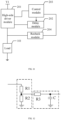
- FIG. 11 is a schematic structural diagram of a drive circuit.
- the drive circuit is configured to drive a load 101, and the load 101 is grounded through a low-side driver module 201.
- the drive circuit of the load also includes a recheck module 204, an input terminal of the recheck module 204 is connected to a second terminal of the high-side driver module 201, and an output terminal of the recheck module 204 is connected to the control module 203.
- the control module 203 is further configured to: at the end of the reset (work resumed), output the drive signal based on a recheck signal input by the recheck module 204, to control the high-side driver module 201.
- the control module 203 can determine a drive signal based on a relay state stored in an internal register of the control module 203. It is assumed that the high-side driver module 201 is shown in FIG. 3 , if the relay is on, the control module outputs a high-level drive signal, a high-level control signal 1, and a high-level control signal 2, to maintain the on state of the relay; and if the relay is off, the control module outputs a low-level drive signal, a low-level control signal 1, and a low-level control signal 2 to maintain the off state of the relay.
- the recheck module 204 includes a voltage divider sub-module and a filter sub-module, a first terminal of the voltage divider sub-module serves as the input terminal of the recheck module 204, a second terminal of the voltage divider sub-module is connected to a first terminal of the filter sub-module, and a second terminal of the filter sub-module serves as the output terminal of the recheck module 204.
- the input terminal of the recheck module 204 may alternatively be connected to a control terminal of the high-side driver module 201, and the control module 203 determines a level of the drive signal output after the reset based on an electrical signal detected by the recheck module 204.
- an edge signal is a falling edge signal is used to show a connection relationship among the recheck module 204, the control module 203, the high-side driver module 201, and the delay module 202.
- the edge signal is a rising edge signal
- a connection relationship among the recheck module 204, the control module 203, the high-side driver module 201, and the delay module 202 is approximately the same as that in a case that the edge signal is the falling edge signal.
- a person skilled in the art can perform implementation with reference to FIG. 12 and FIG. 13 .
- the control module 203 determines a state of the load 101 after the reset based on the recheck signal of the recheck module 204.
- the control module 203 may alternatively output the drive signal based on load state data stored in a storage module at the end of the reset (work resumed). For example, after receiving a switch-on signal or a switch-off instruction, the control module 203 writes a relevant instruction into the register. After the reset, the control module 203 reads the data from the register to determine the state of the load 101 after the reset. The control module 203 may alternatively determine the state of the load 101 based on the recheck signal and the load state data stored in the storage module.
- a method for the control module 203 to keep the state of the load 101 after at the end of the reset (work resumed) is not limited in this embodiment.
- the delay module can output a delay signal to the high-side driver module, so that the high-side driver module remains in a state before the control module is reset, thereby avoiding safety hazards caused by a state change of the high-side driver module due to the reset of the control module.
- the control module can output a drive signal to control the high-side driver module to switch on or off, the drive signal can compete with the output signal of the delay module for power supply, and the high-side driver unit can be switched on when either signal meets the requirement.
- modules in the embodiments are all logical modules.
- a logical unit can be a physical unit or part of a physical unit, or may be implemented by integrating a plurality of physical units.
- units less closely related to resolving of the technical problem mentioned in this application are not introduced, but none of this indicates that there are no other units in the embodiments.
Landscapes
- Engineering & Computer Science (AREA)
- Life Sciences & Earth Sciences (AREA)
- Sustainable Development (AREA)
- Sustainable Energy (AREA)
- Power Engineering (AREA)
- Transportation (AREA)
- Mechanical Engineering (AREA)
- Physics & Mathematics (AREA)
- General Physics & Mathematics (AREA)
- Automation & Control Theory (AREA)
- Electronic Switches (AREA)
- Inverter Devices (AREA)
Claims (10)
- Antriebsschaltung, die so konfiguriert ist, dass sie eine Last (101) basierend auf Steuersignalen von einem Steuermodul (203) antreibt, wobei die Antriebsschaltung ein High-Side-Treibermodul (201) und ein Verzögerungsmodul (202) umfasst,das Verzögerungsmodul (202) so konfiguriert ist, dass es ein Verzögerungssignal von voreingestellter Dauer an das High-Side-Treibermodul (201) ausgibt, wenn das Steuermodul (203) zurückgesetzt wird, unddas High-Side-Treibermodul (201) so konfiguriert ist, dass es: entsprechend dem Verzögerungssignal von voreingestellter Dauer in einem Zustand innerhalb der voreingestellten Dauer verbleibt, wobei der Zustand ein Arbeitszustand des High-Side-Treibermoduls (201) ist, bevor das Steuermodul (203) zurückgesetzt wird, und wobei der Zustand ein Einschalten oder ein Ausschalten umfasst,wobei die voreingestellte Dauer größer als eine Rücksetzzeit des Steuermoduls (203) und kleiner als eine Dauer des Hochpegelantriebs ist, der von der Last (101) toleriert werden kann, und wobei die Antriebsschaltung so konfiguriert ist, dass sie die Last (101) antreibt, und die Last (101) über das High-Side-Treibermodul (201) mit einer Antriebsstromversorgung (V1) verbunden ist,dadurch gekennzeichnet, dassdas High-Side-Treibermodul (201) eine erste High-Side-Treibereinheit und eine zweite High-Side-Treibereinheit umfasst, wobei ein erster Anschluss der ersten High-Side-Treibereinheit und ein erster Anschluss der zweiten High-Side-Treibereinheit beide mit der Antriebsstromversorgung (V1) verbunden sind, ein zweiter Anschluss der ersten High-Side-Treibereinheit und ein zweiter Anschluss der zweiten High-Side-Treibereinheit beide mit einem ersten Anschluss der Last (101) verbunden sind, das Steuermodul (203) mit einem Steueranschluss der ersten High-Side-Treibereinheit verbunden ist, und das Verzögerungsmodul (202) mit einem Steueranschluss der zweiten High-Side-Treibereinheit verbunden ist.
- Antriebsschaltung nach Anspruch 1, wobei das Verzögerungsmodul (202) eine Verzögerungseinheit und eine erste Pull-Up-Einheit umfasst, ein erster gesteuerter Anschluss der Verzögerungseinheit sowohl mit der ersten Pull-Up-Einheit als auch mit einem ersten Ausgangsanschluss des Steuermoduls (203) verbunden ist, ein zweiter gesteuerter Anschluss der Verzögerungseinheit mit einem zweiten Ausgangsanschluss des Steuermoduls (203) verbunden ist, und ein Ausgangsanschluss der Verzögerungseinheit mit einem Steueranschluss des High-Side-Treibermoduls (201) verbunden ist, unddie Verzögerungseinheit konfiguriert ist, um: wenn ein elektrisches Signal eines ersten Pegels an dem ersten gesteuerten Anschluss erfasst wird und ein Flankensignal an dem zweiten gesteuerten Anschluss erfasst wird, ein Verzögerungssignal eines zweiten Pegels auszugeben; und wenn ein elektrisches Signal eines dritten Pegels an dem ersten gesteuerten Anschluss erfasst wird, ein Verzögerungssignal eines vierten Pegels auszugeben;wobei der vierte Pegel ein umgekehrter Pegel des zweiten Pegels ist, der dritte Pegel ein umgekehrter Pegel des ersten Pegels ist, unddas High-Side-Treibermodul (201) eingeschaltet wird, wenn ein elektrisches Signal des zweiten Pegels empfangen wird, und ausgeschaltet wird, wenn ein elektrisches Signal des vierten Pegels empfangen wird.
- Antriebsschaltung nach Anspruch 2, wobei für den Fall, dass das Flankensignal ein ansteigendes Flankensignal ist, das Verzögerungsmodul (202) ferner eine zweite Pull-Up-Einheit umfasst, und die zweite Pull-Up-Einheit mit dem zweiten gesteuerten Anschluss der Verzögerungseinheit verbunden ist.
- Antriebsschaltung nach Anspruch 2 oder 3, wobei die Verzögerungseinheit N kaskadierte Verzögerungskomponenten umfasst, und
erste Eingangsanschlüsse der Verzögerungskomponenten miteinander verbunden sind, wobei eine Verbindung als der erste gesteuerte Anschluss der Verzögerungseinheit dient, ein zweiter Eingangsanschluss einer ersten Verzögerungskomponente mit dem zweiten gesteuerten Anschluss der Verzögerungseinheit verbunden ist, ein zweiter Eingangsanschluss einer (i+1)-ten Verzögerungskomponente mit einem Ausgangsanschluss einer i-ten Verzögerungskomponente verbunden ist, und ein Ausgangsanschluss einer N-ten Verzögerungskomponente als der Ausgangsanschluss der Verzögerungseinheit dient, wobei 1≤i<N, und N eine ganze Zahl größer als 1 ist. - Antriebsschaltung nach einem der Ansprüche 2 bis 4, wobei ein Antriebssignal ein Antriebssignal des zweiten Pegels und ein Antriebssignal des vierten Pegels umfasst, und
das Steuermodul (203) so konfiguriert ist, dass es: nach dem Erfassen eines Einschaltsignals das Antriebssignal des zweiten Pegels an das High-Side-Treibermodul (201) ausgibt, ein Steuersignal des ersten Pegels oder des dritten Pegels an den ersten gesteuerten Anschluss des Verzögerungsmoduls (202) ausgibt, und ein Steuersignal eines fünften Pegels oder ein erstes Pulsbreitenmodulations-PWM-Steuersignal an den zweiten gesteuerten Anschluss des Verzögerungsmoduls (202) ausgibt, und nach dem Erfassen eines Abschaltsignals das Antriebssignal des vierten Pegels an das High-Side-Treibermodul (201) ausgibt und ein Steuersignals des dritten Pegels an den ersten gesteuerten Anschluss und den zweiten gesteuerten Anschluss des Verzögerungsmoduls (202) ausgibt, wobei eine Periode des ersten Pulsbreitenmodulations-PWM-Steuersignals kürzer als die voreingestellte Dauer ist, und wenn das Flankensignal ein ansteigendes Flankensignal ist, der fünfte Pegel ein niedriger Pegel ist, oder wenn das Flankensignal ein abfallendes Flankensignal ist, der fünfte Pegel ein hoher Pegel ist. - Antriebsschaltung nach Anspruch 1, wobei das Steuermodul (203) so konfiguriert ist: nach dem Erkennen eines Einschaltsignals das Antriebssignal des zweiten Pegels oder ein zweites Pulsweitenmodulations-PWM-Steuersignal an die erste High-Side-Treibereinheit ausgibt, ein Steuersignals des ersten Pegels oder des dritten Pegels an den ersten gesteuerten Anschluss des Verzögerungsmoduls (202) ausgibt und ein Steuersignal eines fünften Pegels oder ein drittes Pulsweitenmodulations-PWM-Steuersignal an den zweiten gesteuerten Anschluss des Verzögerungsmoduls (202) ausgibt, und nach dem Erkennen eines Abschaltsignals das Antriebssignal des vierten Pegels an die erste High-Side-Treibereinheit ausgibt und ein Steuersignal des dritten Pegels an den ersten gesteuerten Anschluss und den zweiten gesteuerten Anschluss des Verzögerungsmoduls (202) ausgibt, wobei eine Periode des dritten Pulsweitenmodulations-PWM-Steuersignals kürzer als die voreingestellte Dauer ist, und wenn das Flankensignal ein ansteigendes Flankensignal ist, der fünfte Pegel ein niedriger Pegel ist, oder Wenn das Flankensignal ein fallendes Flankensignal ist, der fünfte Pegel ein hoher Pegel ist.
- Antriebsschaltung nach einem der Ansprüche 1 bis 6, wobei die Antriebsschaltung ferner ein erstes Anti-Rückwärts-Modul und ein zweites Anti-Rückwärts-Modul umfasst, das Verzögerungsmodul (202) über das erste Anti-Rückwärts-Modul mit dem Steueranschluss des High-Side-Treibermoduls (201) verbunden ist und das Steuermodul (203) über das zweite Anti-Rückwärts-Modul mit dem Steueranschluss des High-Side-Treibermoduls (201) verbunden ist.
- Antriebsschaltung nach einem der Ansprüche 1 bis 7, wobei die Antriebsschaltung so konfiguriert ist, dass sie eine Last (101) antreibt, und die Last (101) über das High-Side-Treibermodul (201) mit der Antriebsstromversorgung (V1) verbunden ist, und das Steuermodul (203) ferner so konfiguriert ist, dass es: am Ende des Rücksetzens ein Antriebssignal basierend auf einem von einem Rückprüfmodul (204) eingegebenen Rückprüfsignal oder von in einem Speichermodul gespeicherten Lastzustandsdaten ausgibt, um das High-Side-Treibermodul (201) steuert,
wobei ein Eingangsanschluss des Rückprüfmoduls (204) mit einer Verbindung zwischen dem High-Side-Treibermodul (201) und dem Lastmodul verbunden ist oder mit dem Steueranschluss des High-Side-Treibermoduls (201) verbunden ist, und ein Ausgangsanschluss des Rückprüfmoduls (204) mit dem Steuermodul (203) verbunden ist. - Antriebsschaltung nach Anspruch 8, wobei das Rückprüfmodul (204) ein Spannungsteiler-Teilmodul und ein Filter-Teilmodul umfasst, ein erster Anschluss des Spannungsteiler-Teilmoduls als der Eingangsanschluss des Rückprüfmoduls (204) dient, ein zweiter Anschluss des Spannungsteiler-Teilmoduls mit einem ersten Anschluss des Filter-Teilmoduls verbunden ist, und ein zweiter Anschluss des Filter-Teilmoduls als der Ausgangsanschluss des Rückprüfmoduls (204) dient.
- Verarbeitungsverfahren für eine Antriebsschaltung nach einem der Ansprüche 1 bis 9,
wobei das Verarbeitungsverfahren umfasst:Ausgeben eines Verzögerungssignals mit voreingestellter Dauer durch das Verzögerungsmodul (202) an das High-Side-Treibermodul (201) in einem Fall, in dem ein Steuermodul (203) zurückgesetzt wird, undgemäß dem Verzögerungssignal von voreingestellter Dauer durch das High-Side-Treibermodul (201) in einem Zustand innerhalb der voreingestellten Dauer verbleibt, wobei der Zustand ein Arbeitszustand des High-Side-Treibermoduls (201) ist, bevor das Steuermodul (203) zurückgesetzt wird, und wobei der Zustand ein Einschalten oder ein Ausschalten umfasst,wobei die voreingestellte Dauer größer als eine Rücksetzzeit des Steuermoduls (203) ist und kleiner als eine Dauer der Hochpegelansteuerung ist, die von einer Last (101) toleriert werden kann.
Applications Claiming Priority (2)
| Application Number | Priority Date | Filing Date | Title |
|---|---|---|---|
| CN202010479366.7A CN113752838B (zh) | 2020-05-29 | 2020-05-29 | 一种驱动电路 |
| PCT/CN2021/079608 WO2021238330A1 (zh) | 2020-05-29 | 2021-03-08 | 一种驱动电路 |
Publications (4)
| Publication Number | Publication Date |
|---|---|
| EP4043264A1 EP4043264A1 (de) | 2022-08-17 |
| EP4043264A4 EP4043264A4 (de) | 2023-01-18 |
| EP4043264B1 true EP4043264B1 (de) | 2024-07-03 |
| EP4043264C0 EP4043264C0 (de) | 2024-07-03 |
Family
ID=78745572
Family Applications (1)
| Application Number | Title | Priority Date | Filing Date |
|---|---|---|---|
| EP21814463.2A Active EP4043264B1 (de) | 2020-05-29 | 2021-03-08 | Treiberschaltung |
Country Status (6)
| Country | Link |
|---|---|
| US (1) | US11996833B2 (de) |
| EP (1) | EP4043264B1 (de) |
| CN (1) | CN113752838B (de) |
| ES (1) | ES2990004T3 (de) |
| HU (1) | HUE068206T2 (de) |
| WO (1) | WO2021238330A1 (de) |
Families Citing this family (3)
| Publication number | Priority date | Publication date | Assignee | Title |
|---|---|---|---|---|
| CN114211963B (zh) * | 2021-12-14 | 2023-10-17 | 华人运通(江苏)技术有限公司 | 一种继电器控制装置、电池管理系统及电动汽车 |
| CN114563967B (zh) * | 2022-02-24 | 2024-09-03 | 浙江阳光照明电器集团股份有限公司 | 一种智能插座驱动电路 |
| CN117477916B (zh) * | 2023-12-21 | 2024-03-12 | 拓尔微电子股份有限公司 | 一种低边驱动电路以及电机驱动电路 |
Family Cites Families (20)
| Publication number | Priority date | Publication date | Assignee | Title |
|---|---|---|---|---|
| JP4258420B2 (ja) * | 2004-04-21 | 2009-04-30 | 株式会社デンソー | エンジン始動制御装置 |
| US7800350B2 (en) * | 2007-05-11 | 2010-09-21 | Freescale Semiconductor, Inc. | Apparatus for optimizing diode conduction time during a deadtime interval |
| JP2009268286A (ja) * | 2008-04-28 | 2009-11-12 | Nissan Motor Co Ltd | 電動車両の制御装置及び制御方法 |
| JP5245846B2 (ja) * | 2009-01-15 | 2013-07-24 | トヨタ自動車株式会社 | 動力出力装置およびその制御方法並びにハイブリッド車 |
| JP4835743B2 (ja) * | 2009-10-07 | 2011-12-14 | 株式会社デンソー | 電力変換回路の制御装置 |
| CN205149545U (zh) | 2015-10-13 | 2016-04-13 | 北京波士顿动力电池有限公司 | 一种汽车动力系统安全电路 |
| CN106602900A (zh) * | 2015-10-19 | 2017-04-26 | 中兴通讯股份有限公司 | 一种高低边自举驱动控制方法及装置 |
| CN105490255B (zh) * | 2016-01-11 | 2017-10-27 | 福建省汽车工业集团云度新能源汽车股份有限公司 | 一种bms高边驱动的联动保护及报警电路 |
| KR102121639B1 (ko) | 2016-07-15 | 2020-06-10 | 주식회사 엘지화학 | 실시간 동작 감지를 통한 컨텍터의 비정상 개방 방지 시스템 및 방법 |
| US10784800B2 (en) * | 2016-12-28 | 2020-09-22 | Hitachi Automotive Systems, Ltd. | Signal control apparatus |
| CN107891756B (zh) * | 2017-11-10 | 2019-11-29 | 宁德时代新能源科技股份有限公司 | 开关驱动电路及方法、驱动器、电池装置、运载工具和计算机可读存储介质 |
| CN108183469B (zh) * | 2018-01-02 | 2020-02-07 | 重庆长安汽车股份有限公司 | 一种防止高边驱动电源反接保护电路及整车控制器 |
| CN208867859U (zh) * | 2018-08-10 | 2019-05-17 | 吉利汽车研究院(宁波)有限公司 | 一种具有诊断功能的双边驱动电路及电池包 |
| CN109245053A (zh) * | 2018-08-30 | 2019-01-18 | 广州金升阳科技有限公司 | 一种过载保护电路 |
| KR102617729B1 (ko) * | 2018-09-17 | 2023-12-26 | 삼성에스디아이 주식회사 | 릴레이의 동작 상태를 유지시키는 장치 및 이를 포함하는 전자장치 |
| CN110262297B (zh) * | 2018-09-21 | 2020-10-02 | 宁德时代新能源科技股份有限公司 | 继电器控制装置及供电系统 |
| CN209479429U (zh) * | 2018-12-28 | 2019-10-11 | 蜂巢能源科技有限公司 | 电池管理系统电平信号控制的接触器保持电路 |
| CN209344264U (zh) | 2019-01-04 | 2019-09-03 | 蜂巢能源科技有限公司 | 电池管理系统pwm信号控制的接触器保持电路 |
| CN110962602B (zh) * | 2019-04-15 | 2021-06-15 | 宁德时代新能源科技股份有限公司 | 应用于电池管理系统的负载保持电路 |
| CN209756843U (zh) * | 2019-04-30 | 2019-12-10 | 宁德时代新能源科技股份有限公司 | 一种驱动装置和电池管理系统 |
-
2020
- 2020-05-29 CN CN202010479366.7A patent/CN113752838B/zh active Active
-
2021
- 2021-03-08 EP EP21814463.2A patent/EP4043264B1/de active Active
- 2021-03-08 ES ES21814463T patent/ES2990004T3/es active Active
- 2021-03-08 WO PCT/CN2021/079608 patent/WO2021238330A1/zh not_active Ceased
- 2021-03-08 HU HUE21814463A patent/HUE068206T2/hu unknown
-
2022
- 2022-04-29 US US17/732,569 patent/US11996833B2/en active Active
Also Published As
| Publication number | Publication date |
|---|---|
| WO2021238330A1 (zh) | 2021-12-02 |
| CN113752838A (zh) | 2021-12-07 |
| US11996833B2 (en) | 2024-05-28 |
| EP4043264A1 (de) | 2022-08-17 |
| US20220255546A1 (en) | 2022-08-11 |
| ES2990004T3 (es) | 2024-11-28 |
| HUE068206T2 (hu) | 2024-12-28 |
| CN113752838B (zh) | 2023-10-03 |
| EP4043264A4 (de) | 2023-01-18 |
| EP4043264C0 (de) | 2024-07-03 |
Similar Documents
| Publication | Publication Date | Title |
|---|---|---|
| EP4044208B1 (de) | Treiberschaltung | |
| US11996833B2 (en) | Drive circuit | |
| EP0442688A2 (de) | Schaltkreis | |
| JP4313658B2 (ja) | インバータ回路 | |
| EP0743752A1 (de) | Laden eines Bootstrap-Kondensators mittels eines lateralen DMOS-Transistors | |
| US9871440B2 (en) | Internal power supply circuit and semiconductor device | |
| CN111478302A (zh) | 一种带接反保护的输出驱动电路 | |
| CN112688683B (zh) | 防止感性负载驱动电路被反电动势损坏的装置和方法 | |
| JP2911453B2 (ja) | 誘導負荷を駆動するパワースイッチングトランジスタの電流再循環回路 | |
| CN214626958U (zh) | 防止感性负载驱动电路被反电动势损坏的装置 | |
| US20230117130A1 (en) | Motor inverter | |
| CN114765361A (zh) | 一种过压保护驱动电路、电机驱动电路及车辆 | |
| CN111541217A (zh) | 短路保护电路、电器设备和电气系统 | |
| US12587186B2 (en) | Switch control device and battery pack including the same | |
| CN117767222B (zh) | 直流短路保护电路 | |
| CN220122612U (zh) | 一种限压保护电路 | |
| KR100331831B1 (ko) | 인버터의 파워소자의 제어회로 | |
| CN219144998U (zh) | 一种短路保护电路及开关电源 | |
| CN115021537B (zh) | 一种预驱动电路 | |
| CN213879628U (zh) | 电源驱动电路及电源 | |
| CN214705813U (zh) | 脉冲驱动电路 | |
| CN112736859B (zh) | 过流诊断处理电路以及低边驱动电路 | |
| CN112947655B (zh) | 稳压电路、稳压方法及显示装置 | |
| CN117081556A (zh) | 一种电源控制电路和电动车辆 | |
| KR100239774B1 (ko) | 모터 구동시 기동전류 억제 장치 |
Legal Events
| Date | Code | Title | Description |
|---|---|---|---|
| STAA | Information on the status of an ep patent application or granted ep patent |
Free format text: STATUS: THE INTERNATIONAL PUBLICATION HAS BEEN MADE |
|
| PUAI | Public reference made under article 153(3) epc to a published international application that has entered the european phase |
Free format text: ORIGINAL CODE: 0009012 |
|
| STAA | Information on the status of an ep patent application or granted ep patent |
Free format text: STATUS: REQUEST FOR EXAMINATION WAS MADE |
|
| 17P | Request for examination filed |
Effective date: 20220505 |
|
| AK | Designated contracting states |
Kind code of ref document: A1 Designated state(s): AL AT BE BG CH CY CZ DE DK EE ES FI FR GB GR HR HU IE IS IT LI LT LU LV MC MK MT NL NO PL PT RO RS SE SI SK SM TR |
|
| A4 | Supplementary search report drawn up and despatched |
Effective date: 20221215 |
|
| RIC1 | Information provided on ipc code assigned before grant |
Ipc: H03K 17/28 20060101ALI20221209BHEP Ipc: H03K 17/10 20060101ALI20221209BHEP Ipc: G05B 19/05 20060101ALI20221209BHEP Ipc: H01H 47/32 20060101ALI20221209BHEP Ipc: H01H 83/00 20060101ALI20221209BHEP Ipc: H01H 71/66 20060101ALI20221209BHEP Ipc: H01H 47/18 20060101ALI20221209BHEP Ipc: H01H 47/04 20060101ALI20221209BHEP Ipc: H01H 47/02 20060101ALI20221209BHEP Ipc: H01H 47/00 20060101ALI20221209BHEP Ipc: H01H 7/00 20060101ALI20221209BHEP Ipc: H01H 3/22 20060101ALI20221209BHEP Ipc: H01H 3/00 20060101ALI20221209BHEP Ipc: B60L 3/00 20190101ALI20221209BHEP Ipc: G05B 19/042 20060101ALI20221209BHEP Ipc: B60L 3/04 20060101AFI20221209BHEP |
|
| STAA | Information on the status of an ep patent application or granted ep patent |
Free format text: STATUS: EXAMINATION IS IN PROGRESS |
|
| 17Q | First examination report despatched |
Effective date: 20230711 |
|
| DAV | Request for validation of the european patent (deleted) | ||
| DAX | Request for extension of the european patent (deleted) | ||
| GRAP | Despatch of communication of intention to grant a patent |
Free format text: ORIGINAL CODE: EPIDOSNIGR1 |
|
| STAA | Information on the status of an ep patent application or granted ep patent |
Free format text: STATUS: GRANT OF PATENT IS INTENDED |
|
| GRAS | Grant fee paid |
Free format text: ORIGINAL CODE: EPIDOSNIGR3 |
|
| INTG | Intention to grant announced |
Effective date: 20240430 |
|
| GRAA | (expected) grant |
Free format text: ORIGINAL CODE: 0009210 |
|
| STAA | Information on the status of an ep patent application or granted ep patent |
Free format text: STATUS: THE PATENT HAS BEEN GRANTED |
|
| AK | Designated contracting states |
Kind code of ref document: B1 Designated state(s): AL AT BE BG CH CY CZ DE DK EE ES FI FR GB GR HR HU IE IS IT LI LT LU LV MC MK MT NL NO PL PT RO RS SE SI SK SM TR |
|
| RAP3 | Party data changed (applicant data changed or rights of an application transferred) |
Owner name: CONTEMPORARY AMPEREX TECHNOLOGY CO., LIMITED |
|
| REG | Reference to a national code |
Ref country code: CH Ref legal event code: EP |
|
| REG | Reference to a national code |
Ref country code: DE Ref legal event code: R096 Ref document number: 602021015288 Country of ref document: DE |
|
| U01 | Request for unitary effect filed |
Effective date: 20240726 |
|
| U07 | Unitary effect registered |
Designated state(s): AT BE BG DE DK EE FI FR IT LT LU LV MT NL PT SE SI Effective date: 20240809 |
|
| REG | Reference to a national code |
Ref country code: GB Ref legal event code: 732E Free format text: REGISTERED BETWEEN 20240829 AND 20240904 |
|
| RAP2 | Party data changed (patent owner data changed or rights of a patent transferred) |
Owner name: CONTEMPORARY AMPEREX TECHNOLOGY(HONG KONG) LIMITED |
|
| U1K | Transfer of rights of the unitary patent after the registration of the unitary effect |
Owner name: CONTEMPORARY AMPEREX TECHNOLOGY(HONG KONG) LIMITED; HK |
|
| REG | Reference to a national code |
Ref country code: ES Ref legal event code: FG2A Ref document number: 2990004 Country of ref document: ES Kind code of ref document: T3 Effective date: 20241128 |
|
| REG | Reference to a national code |
Ref country code: HU Ref legal event code: AG4A Ref document number: E068206 Country of ref document: HU |
|
| PG25 | Lapsed in a contracting state [announced via postgrant information from national office to epo] |
Ref country code: NO Free format text: LAPSE BECAUSE OF FAILURE TO SUBMIT A TRANSLATION OF THE DESCRIPTION OR TO PAY THE FEE WITHIN THE PRESCRIBED TIME-LIMIT Effective date: 20241003 |
|
| PG25 | Lapsed in a contracting state [announced via postgrant information from national office to epo] |
Ref country code: PL Free format text: LAPSE BECAUSE OF FAILURE TO SUBMIT A TRANSLATION OF THE DESCRIPTION OR TO PAY THE FEE WITHIN THE PRESCRIBED TIME-LIMIT Effective date: 20240703 Ref country code: GR Free format text: LAPSE BECAUSE OF FAILURE TO SUBMIT A TRANSLATION OF THE DESCRIPTION OR TO PAY THE FEE WITHIN THE PRESCRIBED TIME-LIMIT Effective date: 20241004 |
|
| PG25 | Lapsed in a contracting state [announced via postgrant information from national office to epo] |
Ref country code: IS Free format text: LAPSE BECAUSE OF FAILURE TO SUBMIT A TRANSLATION OF THE DESCRIPTION OR TO PAY THE FEE WITHIN THE PRESCRIBED TIME-LIMIT Effective date: 20241103 |
|
| PG25 | Lapsed in a contracting state [announced via postgrant information from national office to epo] |
Ref country code: HR Free format text: LAPSE BECAUSE OF FAILURE TO SUBMIT A TRANSLATION OF THE DESCRIPTION OR TO PAY THE FEE WITHIN THE PRESCRIBED TIME-LIMIT Effective date: 20240703 Ref country code: CZ Free format text: LAPSE BECAUSE OF FAILURE TO SUBMIT A TRANSLATION OF THE DESCRIPTION OR TO PAY THE FEE WITHIN THE PRESCRIBED TIME-LIMIT Effective date: 20240703 |
|
| PG25 | Lapsed in a contracting state [announced via postgrant information from national office to epo] |
Ref country code: RS Free format text: LAPSE BECAUSE OF FAILURE TO SUBMIT A TRANSLATION OF THE DESCRIPTION OR TO PAY THE FEE WITHIN THE PRESCRIBED TIME-LIMIT Effective date: 20241003 |
|
| PG25 | Lapsed in a contracting state [announced via postgrant information from national office to epo] |
Ref country code: RS Free format text: LAPSE BECAUSE OF FAILURE TO SUBMIT A TRANSLATION OF THE DESCRIPTION OR TO PAY THE FEE WITHIN THE PRESCRIBED TIME-LIMIT Effective date: 20241003 Ref country code: PL Free format text: LAPSE BECAUSE OF FAILURE TO SUBMIT A TRANSLATION OF THE DESCRIPTION OR TO PAY THE FEE WITHIN THE PRESCRIBED TIME-LIMIT Effective date: 20240703 Ref country code: NO Free format text: LAPSE BECAUSE OF FAILURE TO SUBMIT A TRANSLATION OF THE DESCRIPTION OR TO PAY THE FEE WITHIN THE PRESCRIBED TIME-LIMIT Effective date: 20241003 Ref country code: IS Free format text: LAPSE BECAUSE OF FAILURE TO SUBMIT A TRANSLATION OF THE DESCRIPTION OR TO PAY THE FEE WITHIN THE PRESCRIBED TIME-LIMIT Effective date: 20241103 Ref country code: HR Free format text: LAPSE BECAUSE OF FAILURE TO SUBMIT A TRANSLATION OF THE DESCRIPTION OR TO PAY THE FEE WITHIN THE PRESCRIBED TIME-LIMIT Effective date: 20240703 Ref country code: GR Free format text: LAPSE BECAUSE OF FAILURE TO SUBMIT A TRANSLATION OF THE DESCRIPTION OR TO PAY THE FEE WITHIN THE PRESCRIBED TIME-LIMIT Effective date: 20241004 Ref country code: CZ Free format text: LAPSE BECAUSE OF FAILURE TO SUBMIT A TRANSLATION OF THE DESCRIPTION OR TO PAY THE FEE WITHIN THE PRESCRIBED TIME-LIMIT Effective date: 20240703 |
|
| PG25 | Lapsed in a contracting state [announced via postgrant information from national office to epo] |
Ref country code: SM Free format text: LAPSE BECAUSE OF FAILURE TO SUBMIT A TRANSLATION OF THE DESCRIPTION OR TO PAY THE FEE WITHIN THE PRESCRIBED TIME-LIMIT Effective date: 20240703 |
|
| U20 | Renewal fee for the european patent with unitary effect paid |
Year of fee payment: 5 Effective date: 20250318 |
|
| PG25 | Lapsed in a contracting state [announced via postgrant information from national office to epo] |
Ref country code: SK Free format text: LAPSE BECAUSE OF FAILURE TO SUBMIT A TRANSLATION OF THE DESCRIPTION OR TO PAY THE FEE WITHIN THE PRESCRIBED TIME-LIMIT Effective date: 20240703 |
|
| PLBE | No opposition filed within time limit |
Free format text: ORIGINAL CODE: 0009261 |
|
| STAA | Information on the status of an ep patent application or granted ep patent |
Free format text: STATUS: NO OPPOSITION FILED WITHIN TIME LIMIT |
|
| 26N | No opposition filed |
Effective date: 20250404 |
|
| PGFP | Annual fee paid to national office [announced via postgrant information from national office to epo] |
Ref country code: ES Payment date: 20250401 Year of fee payment: 5 |
|
| PG25 | Lapsed in a contracting state [announced via postgrant information from national office to epo] |
Ref country code: MC Free format text: LAPSE BECAUSE OF FAILURE TO SUBMIT A TRANSLATION OF THE DESCRIPTION OR TO PAY THE FEE WITHIN THE PRESCRIBED TIME-LIMIT Effective date: 20240703 |
|
| REG | Reference to a national code |
Ref country code: CH Ref legal event code: H13 Free format text: ST27 STATUS EVENT CODE: U-0-0-H10-H13 (AS PROVIDED BY THE NATIONAL OFFICE) Effective date: 20251024 |
|
| PG25 | Lapsed in a contracting state [announced via postgrant information from national office to epo] |
Ref country code: CH Free format text: LAPSE BECAUSE OF NON-PAYMENT OF DUE FEES Effective date: 20250331 |
|
| PG25 | Lapsed in a contracting state [announced via postgrant information from national office to epo] |
Ref country code: IE Free format text: LAPSE BECAUSE OF NON-PAYMENT OF DUE FEES Effective date: 20250308 |
|
| PGFP | Annual fee paid to national office [announced via postgrant information from national office to epo] |
Ref country code: GB Payment date: 20260325 Year of fee payment: 6 |
|
| PG25 | Lapsed in a contracting state [announced via postgrant information from national office to epo] |
Ref country code: RO Free format text: LAPSE BECAUSE OF FAILURE TO SUBMIT A TRANSLATION OF THE DESCRIPTION OR TO PAY THE FEE WITHIN THE PRESCRIBED TIME-LIMIT Effective date: 20240703 |
|
| PGFP | Annual fee paid to national office [announced via postgrant information from national office to epo] |
Ref country code: HU Payment date: 20260316 Year of fee payment: 6 |
|
| U20 | Renewal fee for the european patent with unitary effect paid |
Year of fee payment: 6 Effective date: 20260325 |