EP4043894B1 - Circuit de chaîne de balayage et procédé correspondant - Google Patents
Circuit de chaîne de balayage et procédé correspondant Download PDFInfo
- Publication number
- EP4043894B1 EP4043894B1 EP22153216.1A EP22153216A EP4043894B1 EP 4043894 B1 EP4043894 B1 EP 4043894B1 EP 22153216 A EP22153216 A EP 22153216A EP 4043894 B1 EP4043894 B1 EP 4043894B1
- Authority
- EP
- European Patent Office
- Prior art keywords
- flip
- flops
- chain
- clock
- edge
- Prior art date
- Legal status (The legal status is an assumption and is not a legal conclusion. Google has not performed a legal analysis and makes no representation as to the accuracy of the status listed.)
- Active
Links
Images

Classifications
-
- G—PHYSICS
- G01—MEASURING; TESTING
- G01R—MEASURING ELECTRIC VARIABLES; MEASURING MAGNETIC VARIABLES
- G01R31/00—Arrangements for testing electric properties; Arrangements for locating electric faults; Arrangements for electrical testing characterised by what is being tested not provided for elsewhere
- G01R31/28—Testing of electronic circuits, e.g. by signal tracer
- G01R31/317—Testing of digital circuits
- G01R31/3177—Testing of logic operation, e.g. by logic analysers
-
- G—PHYSICS
- G01—MEASURING; TESTING
- G01R—MEASURING ELECTRIC VARIABLES; MEASURING MAGNETIC VARIABLES
- G01R31/00—Arrangements for testing electric properties; Arrangements for locating electric faults; Arrangements for electrical testing characterised by what is being tested not provided for elsewhere
- G01R31/28—Testing of electronic circuits, e.g. by signal tracer
- G01R31/317—Testing of digital circuits
- G01R31/3181—Functional testing
- G01R31/3185—Reconfiguring for testing, e.g. LSSD, partitioning
- G01R31/318533—Reconfiguring for testing, e.g. LSSD, partitioning using scanning techniques, e.g. LSSD, Boundary Scan, JTAG
- G01R31/318541—Scan latches or cell details
-
- G—PHYSICS
- G01—MEASURING; TESTING
- G01R—MEASURING ELECTRIC VARIABLES; MEASURING MAGNETIC VARIABLES
- G01R31/00—Arrangements for testing electric properties; Arrangements for locating electric faults; Arrangements for electrical testing characterised by what is being tested not provided for elsewhere
- G01R31/26—Testing of individual semiconductor devices
- G01R31/2601—Apparatus or methods therefor
-
- G—PHYSICS
- G01—MEASURING; TESTING
- G01R—MEASURING ELECTRIC VARIABLES; MEASURING MAGNETIC VARIABLES
- G01R31/00—Arrangements for testing electric properties; Arrangements for locating electric faults; Arrangements for electrical testing characterised by what is being tested not provided for elsewhere
- G01R31/26—Testing of individual semiconductor devices
- G01R31/2607—Circuits therefor
-
- G—PHYSICS
- G01—MEASURING; TESTING
- G01R—MEASURING ELECTRIC VARIABLES; MEASURING MAGNETIC VARIABLES
- G01R31/00—Arrangements for testing electric properties; Arrangements for locating electric faults; Arrangements for electrical testing characterised by what is being tested not provided for elsewhere
- G01R31/28—Testing of electronic circuits, e.g. by signal tracer
- G01R31/2832—Specific tests of electronic circuits not provided for elsewhere
- G01R31/2834—Automated test systems [ATE]; using microprocessors or computers
-
- G—PHYSICS
- G01—MEASURING; TESTING
- G01R—MEASURING ELECTRIC VARIABLES; MEASURING MAGNETIC VARIABLES
- G01R31/00—Arrangements for testing electric properties; Arrangements for locating electric faults; Arrangements for electrical testing characterised by what is being tested not provided for elsewhere
- G01R31/28—Testing of electronic circuits, e.g. by signal tracer
- G01R31/317—Testing of digital circuits
- G01R31/3181—Functional testing
- G01R31/3185—Reconfiguring for testing, e.g. LSSD, partitioning
- G01R31/318533—Reconfiguring for testing, e.g. LSSD, partitioning using scanning techniques, e.g. LSSD, Boundary Scan, JTAG
- G01R31/318552—Clock circuits details
-
- G—PHYSICS
- G01—MEASURING; TESTING
- G01R—MEASURING ELECTRIC VARIABLES; MEASURING MAGNETIC VARIABLES
- G01R31/00—Arrangements for testing electric properties; Arrangements for locating electric faults; Arrangements for electrical testing characterised by what is being tested not provided for elsewhere
- G01R31/28—Testing of electronic circuits, e.g. by signal tracer
- G01R31/317—Testing of digital circuits
- G01R31/3181—Functional testing
- G01R31/3185—Reconfiguring for testing, e.g. LSSD, partitioning
- G01R31/318533—Reconfiguring for testing, e.g. LSSD, partitioning using scanning techniques, e.g. LSSD, Boundary Scan, JTAG
- G01R31/318594—Timing aspects
-
- H—ELECTRICITY
- H03—ELECTRONIC CIRCUITRY
- H03K—PULSE TECHNIQUE
- H03K3/00—Circuits for generating electric pulses; Monostable, bistable or multistable circuits
- H03K3/02—Generators characterised by the type of circuit or by the means used for producing pulses
- H03K3/027—Generators characterised by the type of circuit or by the means used for producing pulses by the use of logic circuits, with internal or external positive feedback
- H03K3/037—Bistable circuits
- H03K3/0372—Bistable circuits of the primary-secondary type
-
- H—ELECTRICITY
- H03—ELECTRONIC CIRCUITRY
- H03K—PULSE TECHNIQUE
- H03K19/00—Logic circuits, i.e. having at least two inputs acting on one output; Inverting circuits
- H03K19/20—Logic circuits, i.e. having at least two inputs acting on one output; Inverting circuits characterised by logic function, e.g. AND, OR, NOR, NOT circuits
- H03K19/21—EXCLUSIVE-OR circuits, i.e. giving output if input signal exists at only one input; COINCIDENCE circuits, i.e. giving output only if all input signals are identical
Definitions
- the description relates to screening techniques for semiconductor devices.
- One or more embodiments can be applied advantageously, yet not exclusively, to semiconductor devices intended for use in the automotive sector; in that sector, automotive system manufacturers expect component suppliers to ship components with 0 ppm, that is, devices having zero failures per million devices.
- HVST dynamic voltage stress at high voltage
- An approach which is often used is based on scan architectures which facilitate stressing various internal nodes of a device.
- Scan chains might face problems related to high-voltage operation in so far as such architectures may be sensitive to "hold” timing violations.
- violations may not be easy to identify or fix. This results in a potentially high area penalty: these violations may in fact correspond to stress conditions outside the functional range dictated by specifications. If such a condition arises, a corresponding library cannot be characterized and this militates against a precise analysis.
- Document US 6 901 544 B1 discloses a circuit comprising a clock circuit and scan chain with a lockup latch which is clocked by inverted (falling) clock edges at the end of the scan chain path in a hard-core to avoid any timing problems which can commonly occur caused by clock skew between the test clock paths in the hard-core and the peripheral circuits integrated therewith.
- An object of one or more embodiments is to contribute in addressing the issues discussed in the foregoing.
- Scan chain architecture may be exemplary of such a circuit.
- One or more embodiments may relate to a corresponding method.
- a scanning method wherein a sampling edge of consecutive flip-flops (FFs) can be set as function of a logic value may be exemplary of such a method.
- One or more embodiments may include a clock inversion logic applied to FFs.
- One or more embodiments may include flip-flops having a pin configured to keep or invert a sampling edge.
- one or more embodiments may involve the addition of a pin (e.g., "CKT") on each flip-flop configured to keep or invert the sampling edge of consecutive flip-flops as a function of a logic value present at that pin.
- CKT a pin
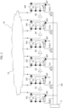
- Scan chains such as the one designated 10 as illustrated in Figure 1 are conventionally used to detect possible faults/defects in a (combinational) logic CL of an electronic circuit (not visible as such for simplicity).
- Automatic test pattern generation facilitates generating stimulus test patterns in such a way that (virtually) all the nodes present in the logic CL are stimulated and verified for manufacturing defects/faults using techniques such as, for instance (among various techniques used to facilitate achieving a desired ppm performance), burn-in and dynamic voltage stress at high voltage (briefly, HVST).
- a basic purpose of scan architecture 10 as illustrated in Figure 1 is to detect faults in the logic CL, both combinational and sequential (the flip-flops), and also in the clock tree. Flips-flops are covered implicitly (they can be detected by implication, in so far as otherwise the scan chain cannot shift) and the combinational logic is tested thanks to the pattern generated.
- a scan chain 10 as illustrated in Figure 1 includes a set of cascaded scan flip-flops 101, 102, 103, 104, 105 and 106 clocked by a clock signal applied via a line Clock to the CK nodes of the flip-flops.
- Such a clock signal can be generated in a manner known to those of skill in the art via a control circuit S.
- the chain 10 may in fact comprise a different number, virtually any plural number of flip-flops.
- flip-flops belonging to a same clock domain that is, sharing a single clock signal
- flip-flops belonging to a same clock domain will be considered throughout for simplicity and ease of understanding; in fact, the discussion herein may apply to scan chains operating with different clock signals/in different clock domains.
- scan flip-flops as illustrated herein internally have a multiplexer M at their input.
- test enable signal (generated in a manner known to those of skill in the art, for instance via the control circuit S - the related connection is not visible for simplicity of representation) applied to test enable nodes TE of the flip-flops determines whether a D (functional) input or a TI (test) input reaches to the output Q of the flip-flop when an active clock edge comes at CK.
- a scan chain which acts as a shift register when the design is in a Shift Test Mode (that is, with the test enable signal TE asserted).
- the first flip-flop of the scan chain is connected to a scan input and the last flip-flop in the scan chain is connected to a scan output.
- Scan chain operation can be regarded as involving three stages, namely scan in (this is the scan_in shift mode phase where the FFs in the chain are loaded through scan in pins serially), capture (the design is kept in functional timing mode and test pattern response is captured) and scan out (this is the scan-out shift mode phase where FFs in the chain are unloaded through scan out pins; scan-in phase can proceed concurrently).
- An issue related to operation of a scan chain 10 as illustrated in Figure 1 may lie in that, e.g., due to the different physical locations of the flip-flops 101 to 106 in the chain, the active clock edges in the clock signal from the control circuit S may arrive at the clock nodes CK of the various flip-flops 101, 102, 103, 104, 105 with different delays. See, for instance, the - purely exemplary - values 0 ns, 1 ns, 3.0 ns, 3.1 ns and 4.6 ns indicated in Figure 1 for the flip-flops 102 to 106. In this - purely exemplary - representation, the flip-flop 101 is assumed to have 0 ns delay.
- signals at the TI (test) inputs may be received during the test mode with different delays D1, D2, D3, D4, D5 (see, for instance, the - purely exemplary - values 0.5 ns, 1.3 ns, 2.1 ns, 0.2 ns and 1.2 ns indicated in Figure 1 for the TI inputs of the flip-flops 102, 103, 104, 105, and 106, respectively.
- Figure 2 represents (merely by way of example with reference to a possible value of t hold equal to 0.2 ns) three possible time behaviors of such a signal against the time behavior of active clock edge coming at CK.
- a possible solution to fix the (hold) time issues discussed in the foregoing may involve adding further buffers such as D1, ..., D5 between the Q and TI nodes of the flip-flops, on top of those added to prevent violations at the design rule checking (DRC), that is to increase the delay Dj in order to meet the rule mentioned in the foregoing.
- DRC design rule checking
- a drawback of this solution may be related to the fact that it is not intrinsically robust.
- hold analysis may be involved in order to facilitate adequate functionality in forecasting a Voltage and Temperature corner (briefly, VT Corner) used in burn-in/dynamic voltage stress conditions.
- threshold cell types i.e., standard Vt (SVT), low Vt (LVT) and ultra-low Vt (ULVT) - the respective derating factors might be different, which undesirably involves a specific analysis.
- SVT standard Vt
- LVT low Vt
- ULVT ultra-low Vt
- a functional Q node may be connected to the functional logic CL only and a scan out node may be connected only to the next test input TI node.
- a scan out driver could be designed with low strength to have a delay in the signal propagation (3ns, for instance).
- possible hold violations between consecutive flip-flops in a scan chain such as 10 can be countered by changing the sampling edges of adjacent subsequent (consecutive) flip-flops in the scan chain.
- a scan chain 10 exemplary of such embodiments is exemplified in Figure 3 .
- a scan chain 10 used for techniques such as burn-in and dynamic voltage stress at high voltage again includes a set of cascaded flip-flops 101, 102, 103, 104, 105 and 106 clocked by a clock signal applied via a line Clock to the CK nodes of the flip-flops.
- the chain 10 may in fact comprise a different number, virtually any plural number of flip-flops.
- a node (pin) CKT is added on each flip-flop 101 to 106 in the chain 10, with the node CKT configured to:
- edge inversion takes place in an alternate sequence, for instance starting from the first flip-flop 101 in the chain.
- the flip-flops 101 to 106 can be regarded as arranged in pairs, namely:
- edge inversion adjacent flip-flops in the chain (here 101 and 102, 102 and 103, 103 and 104, 104 and 105, 105 and 106) will have mutually opposed (inverted) sampling edges.
- the CKT pins of the flip-flops 101 to 106 in the scan chain are coupled to a line TM to which a test mode signal (generated in the control circuit S, for instance) is applied in order to be enabled (only) during high-voltage manufacturing testing.
- a test mode signal generated in the control circuit S, for instance
- such a signal can be both static and dynamic (that is, always active in shift while active or not in capture).
- TM will be generally different from the Test Enable (TE) input to the flip-flops, which goes high when shift is performed, and in capture mode.
- FIG. 3 shows the inputs CKT of the odd-numbered flip-flops 101, 103, 105 (edge inversion) coupled to the line TM and the inputs CKT of the even-numbered flip-flops 102, 104, 106 (no edge inversion) coupled to ground.
- the node CKT at that flip-flop can be regarded as connected to GND insofar as the rule of edge inversion between adjacent flip-flops (with respect to the flip-flops 102 and 104, in the exemplary case considered) is already respected without a connection to CKT.
- One or more embodiments thus rely on the recognition that having edges inverted as discussed previously provides a half-clock-period margin.
- CKhalfperiod can be increased - that is the clock frequency decreased - in order to accommodate Dj and/or the two values for Ckdel10 j and Ckdel10 j+1 to (further) facilitate correct shift operation.
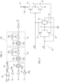
- edge inversion can be integrated in the flip-flops such as 101 to 106 (as represented in Figure 3 , where the inputs CKT of the flip-flops are illustrated coupled alternately to the line TM and to ground) or added as an outer functionality.
- LM and LS indicate (otherwise conventional) latch master and latch slave circuitry providing (e.g., via a logic inverter) the Q output for each flip-flop.
- the EX-OR gate 20 receives at its inputs the signals on the lines Clock (CK) and TM (CKT) and provides an output signal CK1 which (after logic inversion at a logic inverter 30) provides clock signal CK2.
- the signal CK2 can be applied together with CK1 to both the latch master circuitry LM and the latch slave circuitry LS in order to provide the Q output as desired for each flip-flop.
- Figure 5 is a transistor level representation of a possible implementation of the the EX-OR circuitry 20 including three pairs of electronic switches such as MOSFET transistors 31, 32; 41, 42; and 51, 52.
- the transistors 31, 32 in the first pair As exemplified in Figure 5 , the transistors 31, 32 in the first pair:
- the transistors 41, 42 in the second pair As exemplified in Figure 5 , the transistors 41, 42 in the second pair:
- transistors 51, 52 in the third pair As exemplified in Figure 5 , the transistors 51, 52 in the third pair:
- one or more embodiments as exemplified herein may advantageously provide fault coverage of an added CKT signal provided during ATPG manufacturing test.
- One or more embodiments as exemplified herein may effectively address issues related to the fact that voltage stress may represent a challenge in so far as the circuit (logic) being screened is forced to operate (well) above its functional specifications.
- a conventional scan method as currently used to stress a device in such extreme conditions may suffer from drawbacks related to the fact that the scan architecture rely on a hold timing in order to facilitate correct shift operation which may otherwise be critical and area consuming.
- One or more embodiments facilitate overcoming such a limitation via adequate shift operation (also) in these extreme conditions against a reduced area overhead.
- a circuit for instance, 10 as exemplified herein comprises a scan chain of cascaded flip-flops (for instance, 101, 102, 103, 104, 105, 106), the flip-flops in the chain having a functional input node (D) and a test input node (TI) configured to be selectively coupled (for instance, via the multiplexer M actuated by the test enable signal applied to test enable node TE) to logic circuitry (for instance, CL) at a clock edge time (see, for instance, t setup , t hold in Figure 2 ) .
- D functional input node
- TI test input node
- the flip-flops cascaded in the scan chain are configured to selectively (M, TE) couple a functional input node (D) and a test input node (TI) to logic circuitry (CL) the flip-flops being triggered by a clock edge at a clock edge time (t setup , t hold ).
- Clock circuitry for instance, the line designated Clock in the figures
- at least one clock signal (as noted, one or more embodiments may include different clocks) to the flip-flops in the chain, wherein the flip-flops in the chain have active clock edges (CK) applied thereto at respective clock edge times.
- CK active clock edges
- the flip-flops in the chain may comprise a set (for instance, 101, 103, 105) of flip-flops configured to receive an edge inversion signal (for instance, TM) and to selectively invert said active clock edges in response to said edge inversion signal being asserted.
- an edge inversion signal for instance, TM
- said set of flip-flops may consist of non-adjacent flip-flops in the chain (for instance, 101, 103 and 105).
- said set of flip-flops may consist of alternate flip-flops in the chain (for instance, flip-flops 101, 103 and 105) wherein each flip-flop in said set has one or two adjacent flip-flops in the chain configured to maintain said active clock edges irrespective of said edge inversion signal being asserted.
- the flip-flops in said set (for instance, 101, 103, 105) comprise logic circuitry configured to receive said edge inversion signal and to invert said active clock edge in response to said edge inversion signal being asserted.
- said logic circuitry may comprise EX-OR logic circuitry.
- a method as exemplified herein comprises coupling to logic circuitry (for instance, CL) at a clock edge time (see, for instance, t setup , t hold in Figure 2 ) an input node selected (for instance, via the multiplexer M actuated by the test enable signal applied to test enable node TE) out of a functional input node (for instance, D) and a test input node (for instance, TI) in the flip-flops of a scan chain of cascaded flip-flops (for instance, 101, 102, 103, 104, 105, 106).
- logic circuitry for instance, CL
- a clock edge time see, for instance, t setup , t hold in Figure 2
- an input node selected for instance, via the multiplexer M actuated by the test enable signal applied to test enable node TE
- a functional input node for instance, D
- a test input node for instance, TI
- a method as exemplified herein comprises selectively coupling to logic circuitry CL at a clock edge time t setup , t hold an input node selected (M, TE) out of a functional input node (D) and a test input node (TI) in the flip-flops of a scan chain of cascaded flip-flops (101, 102, 103, 104, 105, 106), the flip-flops being triggered by a clock edge at a clock edge time (t setup , t hold ).
- a method as exemplified herein comprises distributing at least one clock signal (as noted, one or more embodiments may include different clocks) to the flip-flops in the chain, wherein the flip-flops in the chain have active clock edges applied thereto at respective clock edge times.
- a method as exemplified herein may comprise applying an edge inversion signal (for instance, TM) to a set of flip-flops (for instance, 101, 103, 105) in the chain to selectively invert said active clock edge applied thereto.
- an edge inversion signal for instance, TM
- flip-flops for instance, 101, 103, 105
- said edge inversion signal may be applied to said set of flip-flops in the chain during high-voltage and/or temperature testing (for instance, during burn-in and dynamic voltage stress at high voltage - HVST) of said logic circuitry (for instance, CL) .
- a method as exemplified herein may comprise reducing the frequency of said at least one clock signal (for instance, Clock) distributed to the flip-flops in the chain, with said edge inversion signal applied to said set of flip-flops in the chain.
- Clock for instance, Clock
- reducing the frequency of the clock signal namely increasing CKhalfperiod
- edge inversion signal when the edge inversion signal is applied to these flip-flops facilitates accommodating Dj and/or the two values for Ckdel10 j and Ckdel10 j+1 in the relationship: Ckdel 10 j + D j ⁇ Ckhalfperiod + Ckdel 10 j + 1 + t setup introduced in the foregoing, which results in correct shift operation.
- a method exemplified herein may comprise applying said edge inversion signal to a set (101, 103, 105) of non-adjacent flip-flops in the chain (for instance 101, 103 and 105 out of 101, 102, 103, 104, 105, 106).
- a method as exemplified herein may comprise applying said edge inversion signal to a set of alternate flip-flops in the chain wherein each flip-flop in said set (101, 103, 105) has one or two adjacent flip-flops in the chain configured to maintain said active clock edges (as exemplified by being coupled to ground in Figure 3 ).
Landscapes
- Physics & Mathematics (AREA)
- General Physics & Mathematics (AREA)
- Engineering & Computer Science (AREA)
- General Engineering & Computer Science (AREA)
- Computer Hardware Design (AREA)
- Microelectronics & Electronic Packaging (AREA)
- Tests Of Electronic Circuits (AREA)
- Semiconductor Integrated Circuits (AREA)
Claims (10)
- Circuit (10), comprenant :une chaîne de balayage de bascules en cascade (101, 102, 103, 104, 105, 106), les bascules dans la chaîne étant configurées pour coupler sélectivement (M, TE) un noeud d'entrée fonctionnelle (D) et un noeud d'entrée de test (TI) à une circuiterie logique (CL), lesdites bascules étant déclenchées par un flanc d'horloge à un instant de flanc d'horloge (tsetup, thold),une circuiterie d'horloge (Clock) configurée pour distribuer au moins un signal d'horloge aux bascules dans la chaîne (101, 102, 103, 104, 105, 106), les bascules dans la chaîne (101, 102, 103, 104, 105, 106) ayant des flancs d'horloge actifs (CK) qui leur sont appliqués à des instants de flanc d'horloge respectifs,le circuit (10) étant caractérisé en ce que les bascules dans la chaîne (101, 102, 103, 104, 105, 106) comprennent un ensemble (101, 103, 105) de bascules configurées pour recevoir un signal d'inversion de flanc (TM) et pour inverser sélectivement lesdits flancs d'horloge actifs (CKT) en réponse au fait que ledit signal d'inversion de flanc (TM) est activé.
- Circuit (10) selon la revendication 1, dans lequel ledit ensemble (101, 103, 105) de bascules est constitué de bascules non adjacentes dans la chaîne (101, 102, 103, 104, 105, 106).
- Circuit (10) selon la revendication 1 ou la revendication 2, dans lequel ledit ensemble (101, 103, 105) de bascules est constitué de bascules alternées dans la chaîne (101, 102, 103, 104, 105, 106), chaque bascule dans ledit ensemble (101, 103, 105) ayant une ou deux bascules adjacentes dans la chaîne (102 ; 102, 104 ; 104, 106) configurées pour maintenir lesdits flancs d'horloge actifs (CK) indépendamment du fait que ledit signal d'inversion de flanc (TM) est activé.
- Circuit (10) selon n'importe laquelle des revendications précédentes, dans lequel les bascules dans ledit ensemble (101, 103, 105) comprennent une circuiterie logique (20, 30) configurée pour recevoir ledit signal d'inversion de flanc (TM) et pour inverser ledit flanc d'horloge actif (CKT) en réponse au fait que ledit signal d'inversion de flanc (TM) est activé.
- Circuit (10) selon la revendication 4, dans lequel ladite circuiterie logique (20, 30) comprend une circuiterie logique OU EXCLUSIF (20).
- Procédé, comprenant :le couplage sélectif, à une circuiterie logique (CL), d'un noeud d'entrée sélectionné (M, TE) parmi un noeud d'entrée fonctionnelle (D) et un noeud d'entrée de test (TI) dans les bascules d'une chaîne de balayage de bascules en cascade (101, 102, 103, 104, 105, 106), lesdites bascules étant déclenchées par un flanc d'horloge à un instant de flanc d'horloge (tsetup, thold),la distribution d'au moins un signal d'horloge aux bascules dans la chaîne (101, 102, 103, 104, 105, 106), les bascules dans la chaîne (101, 102, 103, 104, 105, 106) ayant des flancs d'horloge actifs (CK) qui leur sont appliqués à des instants de flanc d'horloge respectifs,le procédé étant caractérisé par l'application d'un signal d'inversion de flanc (TM) à un ensemble de bascules (101, 103, 105) dans la chaîne (101, 102, 103, 104, 105, 106) pour inverser sélectivement ledit flanc d'horloge actif qui leur est appliqué.
- Procédé selon la revendication 6, comprenant l'application dudit signal d'inversion de flanc (TM) audit ensemble de bascules (101, 103, 105) dans la chaîne (101, 102, 103, 104, 105, 106) durant un test à haute tension et/ou haute température de ladite circuiterie logique (CL).
- Procédé selon la revendication 6 ou la revendication 7, comprenant la réduction de la fréquence dudit au moins un signal d'horloge (Clock) distribué aux bascules dans la chaîne (101, 102, 103, 104, 105, 106), avec ledit signal d'inversion de flanc (TM) appliqué audit ensemble de bascules (101, 103, 105) dans la chaîne (10).
- Procédé selon n'importe laquelle des revendications 6 à 8, comprenant l'application dudit signal d'inversion de flanc (TM) à un ensemble (101, 103, 105) de bascules non adjacentes dans la chaîne (101, 102, 103, 104, 105, 106).
- Procédé selon n'importe laquelle des revendications 6 à 9, comprenant l'application dudit signal d'inversion de flanc (TM) à un ensemble (101, 103, 105) de bascules alternées dans la chaîne (101, 102, 103, 104, 105, 106), chaque bascule dans ledit ensemble (101, 103, 105) ayant une ou deux bascules adjacentes dans la chaîne (102 ; 102, 104 ; 104, 106) configurées pour maintenir lesdits flancs d'horloge actifs (CK).
Applications Claiming Priority (1)
| Application Number | Priority Date | Filing Date | Title |
|---|---|---|---|
| IT202100003536 | 2021-02-16 |
Publications (2)
| Publication Number | Publication Date |
|---|---|
| EP4043894A1 EP4043894A1 (fr) | 2022-08-17 |
| EP4043894B1 true EP4043894B1 (fr) | 2023-09-13 |
Family
ID=75539861
Family Applications (1)
| Application Number | Title | Priority Date | Filing Date |
|---|---|---|---|
| EP22153216.1A Active EP4043894B1 (fr) | 2021-02-16 | 2022-01-25 | Circuit de chaîne de balayage et procédé correspondant |
Country Status (3)
| Country | Link |
|---|---|
| US (2) | US11747398B2 (fr) |
| EP (1) | EP4043894B1 (fr) |
| CN (1) | CN114966354B (fr) |
Families Citing this family (2)
| Publication number | Priority date | Publication date | Assignee | Title |
|---|---|---|---|---|
| EP4043894B1 (fr) * | 2021-02-16 | 2023-09-13 | STMicroelectronics S.r.l. | Circuit de chaîne de balayage et procédé correspondant |
| US20240143880A1 (en) * | 2022-11-01 | 2024-05-02 | Taiwan Semiconductor Manufacturing Company, Ltd. | Integrated circuit design method and system |
Family Cites Families (21)
| Publication number | Priority date | Publication date | Assignee | Title |
|---|---|---|---|---|
| US6901544B1 (en) | 2001-10-24 | 2005-05-31 | Lsi Logic Corporation | Scan chain testing of integrated circuits with hard-cores |
| JP4406519B2 (ja) * | 2001-12-03 | 2010-01-27 | 株式会社日立製作所 | 半導体集積回路装置 |
| US6639443B1 (en) * | 2002-04-22 | 2003-10-28 | Broadcom Corporation | Conditional clock buffer circuit |
| US7447961B2 (en) * | 2004-07-29 | 2008-11-04 | Marvell International Ltd. | Inversion of scan clock for scan cells |
| US7831877B2 (en) * | 2007-03-08 | 2010-11-09 | Silicon Image, Inc. | Circuitry to prevent peak power problems during scan shift |
| US7913131B2 (en) * | 2008-01-07 | 2011-03-22 | Arm Limited | Scan chain cell with delay testing capability |
| JP2009222644A (ja) * | 2008-03-18 | 2009-10-01 | Toshiba Corp | 半導体集積回路、及び設計自動化システム |
| JP5182011B2 (ja) * | 2008-10-27 | 2013-04-10 | 富士通セミコンダクター株式会社 | 半導体装置及び半導体装置の試験方法 |
| CN101846724B (zh) * | 2009-03-26 | 2013-06-12 | 台湾积体电路制造股份有限公司 | 用于诊断集成电路的方法和装置 |
| US8258775B2 (en) * | 2009-04-15 | 2012-09-04 | Via Technologies, Inc. | Method and apparatus for determining phase error between clock signals |
| JP2011002261A (ja) * | 2009-06-16 | 2011-01-06 | Renesas Electronics Corp | スキャンテスト回路、その設計方法、およびプログラム |
| US8866527B1 (en) | 2010-04-02 | 2014-10-21 | Altera Corporation | Integrated circuits with hold time avoidance circuitry |
| US9239360B2 (en) * | 2014-01-28 | 2016-01-19 | Texas Instruments Incorporated | DFT approach to enable faster scan chain diagnosis |
| US20150241219A1 (en) | 2014-02-25 | 2015-08-27 | Ford Global Technologies, Llc | Method and Apparatus for Providing a Navigation Route Having Multiple Associated Points of Interest |
| US9473117B2 (en) * | 2015-02-13 | 2016-10-18 | Samsung Electronics Co., Ltd. | Multi-bit flip-flops and scan chain circuits |
| US9941882B1 (en) * | 2016-07-18 | 2018-04-10 | Altera Corporation | Tristate multiplexers with immunity to aging effects |
| US9960705B1 (en) * | 2016-12-14 | 2018-05-01 | Infineon Technologies Ag | Rectifier device with stand-by detection capability |
| US10491197B2 (en) * | 2017-09-20 | 2019-11-26 | Apple Inc. | Flop circuit with integrated clock gating circuit |
| IT201800005810A1 (it) * | 2018-05-29 | 2019-11-29 | Circuito ad auto-test, dispositivo, veicolo e procedimento corrispondenti | |
| EP4043894B1 (fr) * | 2021-02-16 | 2023-09-13 | STMicroelectronics S.r.l. | Circuit de chaîne de balayage et procédé correspondant |
| JP2023040646A (ja) * | 2021-09-10 | 2023-03-23 | キオクシア株式会社 | 半導体装置及び半導体装置の検査方法 |
-
2022
- 2022-01-25 EP EP22153216.1A patent/EP4043894B1/fr active Active
- 2022-02-04 US US17/665,247 patent/US11747398B2/en active Active
- 2022-02-15 CN CN202210136939.5A patent/CN114966354B/zh active Active
-
2023
- 2023-07-18 US US18/354,501 patent/US12203984B2/en active Active
Also Published As
| Publication number | Publication date |
|---|---|
| US12203984B2 (en) | 2025-01-21 |
| CN114966354B (zh) | 2025-10-28 |
| US11747398B2 (en) | 2023-09-05 |
| CN114966354A (zh) | 2022-08-30 |
| EP4043894A1 (fr) | 2022-08-17 |
| US20220263499A1 (en) | 2022-08-18 |
| US20230358806A1 (en) | 2023-11-09 |
Similar Documents
| Publication | Publication Date | Title |
|---|---|---|
| US6239611B1 (en) | Circuit and method for testing whether a programmable logic device complies with a zero-hold-time requirement | |
| US8464117B2 (en) | System for testing integrated circuit with asynchronous clock domains | |
| US6389566B1 (en) | Edge-triggered scan flip-flop and one-pass scan synthesis methodology | |
| US12203984B2 (en) | Scan chain circuit and corresponding method | |
| JP2012516629A (ja) | 性能監視用クリティカルパス回路 | |
| KR20110117589A (ko) | 스캔 시프트 동작 동안 ivd를 감소시키는 시스템 및 장치 | |
| JPH05273311A (ja) | 論理集積回路 | |
| US6853212B2 (en) | Gated scan output flip-flop | |
| US20110066906A1 (en) | Pulse Triggered Latches with Scan Functionality | |
| US7613969B2 (en) | Method and system for clock skew independent scan register chains | |
| US7880498B2 (en) | Adjustable hold flip flop and method for adjusting hold requirements | |
| US8375265B1 (en) | Delay fault testing using distributed clock dividers | |
| US6271700B1 (en) | Semiconductor integrated circuit having scan path | |
| US11366162B2 (en) | Scan output flip-flop with power saving feature | |
| US5898702A (en) | Mutual exclusivity circuit for use in test pattern application scan architecture circuits | |
| US7600167B2 (en) | Flip-flop, shift register, and scan test circuit | |
| JP2005300308A (ja) | 半導体集積回路 | |
| KR101047533B1 (ko) | 멀티 페이즈 스캔체인을 구동하는 시스템온칩과 그 방법 | |
| CN117686879A (zh) | 扫描测试电路、数字芯片、电子设备及功耗降低方法 | |
| KR100294718B1 (ko) | 선형 귀환 시프트 레지스터 및 반도체 집적 회로 장치 | |
| JP2918730B2 (ja) | デジタル論理装置のスキャン回路 | |
| US20240111934A1 (en) | Design for testability for fault detection in clock gate control circuits | |
| US20250096783A1 (en) | Bi-directional scan flip-flop circuit and method | |
| EP4390413A1 (fr) | Conception de test pour interfaces synchrones de source | |
| JP2826408B2 (ja) | 半導体論理集積回路 |
Legal Events
| Date | Code | Title | Description |
|---|---|---|---|
| PUAI | Public reference made under article 153(3) epc to a published international application that has entered the european phase |
Free format text: ORIGINAL CODE: 0009012 |
|
| STAA | Information on the status of an ep patent application or granted ep patent |
Free format text: STATUS: THE APPLICATION HAS BEEN PUBLISHED |
|
| AK | Designated contracting states |
Kind code of ref document: A1 Designated state(s): AL AT BE BG CH CY CZ DE DK EE ES FI FR GB GR HR HU IE IS IT LI LT LU LV MC MK MT NL NO PL PT RO RS SE SI SK SM TR |
|
| STAA | Information on the status of an ep patent application or granted ep patent |
Free format text: STATUS: REQUEST FOR EXAMINATION WAS MADE |
|
| 17P | Request for examination filed |
Effective date: 20221021 |
|
| RBV | Designated contracting states (corrected) |
Designated state(s): AL AT BE BG CH CY CZ DE DK EE ES FI FR GB GR HR HU IE IS IT LI LT LU LV MC MK MT NL NO PL PT RO RS SE SI SK SM TR |
|
| GRAP | Despatch of communication of intention to grant a patent |
Free format text: ORIGINAL CODE: EPIDOSNIGR1 |
|
| STAA | Information on the status of an ep patent application or granted ep patent |
Free format text: STATUS: GRANT OF PATENT IS INTENDED |
|
| INTG | Intention to grant announced |
Effective date: 20230428 |
|
| RIN1 | Information on inventor provided before grant (corrected) |
Inventor name: CASARSA, MARCO |
|
| GRAS | Grant fee paid |
Free format text: ORIGINAL CODE: EPIDOSNIGR3 |
|
| GRAA | (expected) grant |
Free format text: ORIGINAL CODE: 0009210 |
|
| STAA | Information on the status of an ep patent application or granted ep patent |
Free format text: STATUS: THE PATENT HAS BEEN GRANTED |
|
| AK | Designated contracting states |
Kind code of ref document: B1 Designated state(s): AL AT BE BG CH CY CZ DE DK EE ES FI FR GB GR HR HU IE IS IT LI LT LU LV MC MK MT NL NO PL PT RO RS SE SI SK SM TR |
|
| REG | Reference to a national code |
Ref country code: CH Ref legal event code: EP |
|
| REG | Reference to a national code |
Ref country code: DE Ref legal event code: R096 Ref document number: 602022000470 Country of ref document: DE |
|
| REG | Reference to a national code |
Ref country code: IE Ref legal event code: FG4D |
|
| REG | Reference to a national code |
Ref country code: LT Ref legal event code: MG9D |
|
| REG | Reference to a national code |
Ref country code: NL Ref legal event code: MP Effective date: 20230913 |
|
| PG25 | Lapsed in a contracting state [announced via postgrant information from national office to epo] |
Ref country code: GR Free format text: LAPSE BECAUSE OF FAILURE TO SUBMIT A TRANSLATION OF THE DESCRIPTION OR TO PAY THE FEE WITHIN THE PRESCRIBED TIME-LIMIT Effective date: 20231214 |
|
| PG25 | Lapsed in a contracting state [announced via postgrant information from national office to epo] |
Ref country code: SE Free format text: LAPSE BECAUSE OF FAILURE TO SUBMIT A TRANSLATION OF THE DESCRIPTION OR TO PAY THE FEE WITHIN THE PRESCRIBED TIME-LIMIT Effective date: 20230913 Ref country code: RS Free format text: LAPSE BECAUSE OF FAILURE TO SUBMIT A TRANSLATION OF THE DESCRIPTION OR TO PAY THE FEE WITHIN THE PRESCRIBED TIME-LIMIT Effective date: 20230913 Ref country code: NO Free format text: LAPSE BECAUSE OF FAILURE TO SUBMIT A TRANSLATION OF THE DESCRIPTION OR TO PAY THE FEE WITHIN THE PRESCRIBED TIME-LIMIT Effective date: 20231213 Ref country code: LV Free format text: LAPSE BECAUSE OF FAILURE TO SUBMIT A TRANSLATION OF THE DESCRIPTION OR TO PAY THE FEE WITHIN THE PRESCRIBED TIME-LIMIT Effective date: 20230913 Ref country code: LT Free format text: LAPSE BECAUSE OF FAILURE TO SUBMIT A TRANSLATION OF THE DESCRIPTION OR TO PAY THE FEE WITHIN THE PRESCRIBED TIME-LIMIT Effective date: 20230913 Ref country code: HR Free format text: LAPSE BECAUSE OF FAILURE TO SUBMIT A TRANSLATION OF THE DESCRIPTION OR TO PAY THE FEE WITHIN THE PRESCRIBED TIME-LIMIT Effective date: 20230913 Ref country code: GR Free format text: LAPSE BECAUSE OF FAILURE TO SUBMIT A TRANSLATION OF THE DESCRIPTION OR TO PAY THE FEE WITHIN THE PRESCRIBED TIME-LIMIT Effective date: 20231214 Ref country code: FI Free format text: LAPSE BECAUSE OF FAILURE TO SUBMIT A TRANSLATION OF THE DESCRIPTION OR TO PAY THE FEE WITHIN THE PRESCRIBED TIME-LIMIT Effective date: 20230913 |
|
| REG | Reference to a national code |
Ref country code: AT Ref legal event code: MK05 Ref document number: 1611806 Country of ref document: AT Kind code of ref document: T Effective date: 20230913 |
|
| PG25 | Lapsed in a contracting state [announced via postgrant information from national office to epo] |
Ref country code: NL Free format text: LAPSE BECAUSE OF FAILURE TO SUBMIT A TRANSLATION OF THE DESCRIPTION OR TO PAY THE FEE WITHIN THE PRESCRIBED TIME-LIMIT Effective date: 20230913 |
|
| PG25 | Lapsed in a contracting state [announced via postgrant information from national office to epo] |
Ref country code: IS Free format text: LAPSE BECAUSE OF FAILURE TO SUBMIT A TRANSLATION OF THE DESCRIPTION OR TO PAY THE FEE WITHIN THE PRESCRIBED TIME-LIMIT Effective date: 20240113 |
|
| PG25 | Lapsed in a contracting state [announced via postgrant information from national office to epo] |
Ref country code: AT Free format text: LAPSE BECAUSE OF FAILURE TO SUBMIT A TRANSLATION OF THE DESCRIPTION OR TO PAY THE FEE WITHIN THE PRESCRIBED TIME-LIMIT Effective date: 20230913 |
|
| PG25 | Lapsed in a contracting state [announced via postgrant information from national office to epo] |
Ref country code: ES Free format text: LAPSE BECAUSE OF FAILURE TO SUBMIT A TRANSLATION OF THE DESCRIPTION OR TO PAY THE FEE WITHIN THE PRESCRIBED TIME-LIMIT Effective date: 20230913 |
|
| PG25 | Lapsed in a contracting state [announced via postgrant information from national office to epo] |
Ref country code: SM Free format text: LAPSE BECAUSE OF FAILURE TO SUBMIT A TRANSLATION OF THE DESCRIPTION OR TO PAY THE FEE WITHIN THE PRESCRIBED TIME-LIMIT Effective date: 20230913 Ref country code: RO Free format text: LAPSE BECAUSE OF FAILURE TO SUBMIT A TRANSLATION OF THE DESCRIPTION OR TO PAY THE FEE WITHIN THE PRESCRIBED TIME-LIMIT Effective date: 20230913 Ref country code: IS Free format text: LAPSE BECAUSE OF FAILURE TO SUBMIT A TRANSLATION OF THE DESCRIPTION OR TO PAY THE FEE WITHIN THE PRESCRIBED TIME-LIMIT Effective date: 20240113 Ref country code: ES Free format text: LAPSE BECAUSE OF FAILURE TO SUBMIT A TRANSLATION OF THE DESCRIPTION OR TO PAY THE FEE WITHIN THE PRESCRIBED TIME-LIMIT Effective date: 20230913 Ref country code: EE Free format text: LAPSE BECAUSE OF FAILURE TO SUBMIT A TRANSLATION OF THE DESCRIPTION OR TO PAY THE FEE WITHIN THE PRESCRIBED TIME-LIMIT Effective date: 20230913 Ref country code: CZ Free format text: LAPSE BECAUSE OF FAILURE TO SUBMIT A TRANSLATION OF THE DESCRIPTION OR TO PAY THE FEE WITHIN THE PRESCRIBED TIME-LIMIT Effective date: 20230913 Ref country code: AT Free format text: LAPSE BECAUSE OF FAILURE TO SUBMIT A TRANSLATION OF THE DESCRIPTION OR TO PAY THE FEE WITHIN THE PRESCRIBED TIME-LIMIT Effective date: 20230913 Ref country code: PT Free format text: LAPSE BECAUSE OF FAILURE TO SUBMIT A TRANSLATION OF THE DESCRIPTION OR TO PAY THE FEE WITHIN THE PRESCRIBED TIME-LIMIT Effective date: 20240115 Ref country code: SK Free format text: LAPSE BECAUSE OF FAILURE TO SUBMIT A TRANSLATION OF THE DESCRIPTION OR TO PAY THE FEE WITHIN THE PRESCRIBED TIME-LIMIT Effective date: 20230913 |
|
| PG25 | Lapsed in a contracting state [announced via postgrant information from national office to epo] |
Ref country code: PL Free format text: LAPSE BECAUSE OF FAILURE TO SUBMIT A TRANSLATION OF THE DESCRIPTION OR TO PAY THE FEE WITHIN THE PRESCRIBED TIME-LIMIT Effective date: 20230913 Ref country code: IT Free format text: LAPSE BECAUSE OF FAILURE TO SUBMIT A TRANSLATION OF THE DESCRIPTION OR TO PAY THE FEE WITHIN THE PRESCRIBED TIME-LIMIT Effective date: 20230913 |
|
| REG | Reference to a national code |
Ref country code: DE Ref legal event code: R097 Ref document number: 602022000470 Country of ref document: DE |
|
| PG25 | Lapsed in a contracting state [announced via postgrant information from national office to epo] |
Ref country code: DK Free format text: LAPSE BECAUSE OF FAILURE TO SUBMIT A TRANSLATION OF THE DESCRIPTION OR TO PAY THE FEE WITHIN THE PRESCRIBED TIME-LIMIT Effective date: 20230913 |
|
| PLBE | No opposition filed within time limit |
Free format text: ORIGINAL CODE: 0009261 |
|
| STAA | Information on the status of an ep patent application or granted ep patent |
Free format text: STATUS: NO OPPOSITION FILED WITHIN TIME LIMIT |
|
| PG25 | Lapsed in a contracting state [announced via postgrant information from national office to epo] |
Ref country code: DK Free format text: LAPSE BECAUSE OF FAILURE TO SUBMIT A TRANSLATION OF THE DESCRIPTION OR TO PAY THE FEE WITHIN THE PRESCRIBED TIME-LIMIT Effective date: 20230913 |
|
| 26N | No opposition filed |
Effective date: 20240614 |
|
| PG25 | Lapsed in a contracting state [announced via postgrant information from national office to epo] |
Ref country code: MC Free format text: LAPSE BECAUSE OF FAILURE TO SUBMIT A TRANSLATION OF THE DESCRIPTION OR TO PAY THE FEE WITHIN THE PRESCRIBED TIME-LIMIT Effective date: 20230913 |
|
| PG25 | Lapsed in a contracting state [announced via postgrant information from national office to epo] |
Ref country code: MC Free format text: LAPSE BECAUSE OF FAILURE TO SUBMIT A TRANSLATION OF THE DESCRIPTION OR TO PAY THE FEE WITHIN THE PRESCRIBED TIME-LIMIT Effective date: 20230913 |
|
| PG25 | Lapsed in a contracting state [announced via postgrant information from national office to epo] |
Ref country code: LU Free format text: LAPSE BECAUSE OF NON-PAYMENT OF DUE FEES Effective date: 20240125 |
|
| PG25 | Lapsed in a contracting state [announced via postgrant information from national office to epo] |
Ref country code: LU Free format text: LAPSE BECAUSE OF NON-PAYMENT OF DUE FEES Effective date: 20240125 |
|
| PG25 | Lapsed in a contracting state [announced via postgrant information from national office to epo] |
Ref country code: BE Free format text: LAPSE BECAUSE OF NON-PAYMENT OF DUE FEES Effective date: 20240131 |
|
| PG25 | Lapsed in a contracting state [announced via postgrant information from national office to epo] |
Ref country code: FR Free format text: LAPSE BECAUSE OF NON-PAYMENT OF DUE FEES Effective date: 20240131 |
|
| PG25 | Lapsed in a contracting state [announced via postgrant information from national office to epo] |
Ref country code: SI Free format text: LAPSE BECAUSE OF FAILURE TO SUBMIT A TRANSLATION OF THE DESCRIPTION OR TO PAY THE FEE WITHIN THE PRESCRIBED TIME-LIMIT Effective date: 20230913 |
|
| PG25 | Lapsed in a contracting state [announced via postgrant information from national office to epo] |
Ref country code: SI Free format text: LAPSE BECAUSE OF FAILURE TO SUBMIT A TRANSLATION OF THE DESCRIPTION OR TO PAY THE FEE WITHIN THE PRESCRIBED TIME-LIMIT Effective date: 20230913 Ref country code: FR Free format text: LAPSE BECAUSE OF NON-PAYMENT OF DUE FEES Effective date: 20240131 Ref country code: BE Free format text: LAPSE BECAUSE OF NON-PAYMENT OF DUE FEES Effective date: 20240131 |
|
| REG | Reference to a national code |
Ref country code: BE Ref legal event code: MM Effective date: 20240131 |
|
| PG25 | Lapsed in a contracting state [announced via postgrant information from national office to epo] |
Ref country code: BG Free format text: LAPSE BECAUSE OF FAILURE TO SUBMIT A TRANSLATION OF THE DESCRIPTION OR TO PAY THE FEE WITHIN THE PRESCRIBED TIME-LIMIT Effective date: 20230913 |
|
| PG25 | Lapsed in a contracting state [announced via postgrant information from national office to epo] |
Ref country code: BG Free format text: LAPSE BECAUSE OF FAILURE TO SUBMIT A TRANSLATION OF THE DESCRIPTION OR TO PAY THE FEE WITHIN THE PRESCRIBED TIME-LIMIT Effective date: 20230913 |
|
| PG25 | Lapsed in a contracting state [announced via postgrant information from national office to epo] |
Ref country code: IE Free format text: LAPSE BECAUSE OF NON-PAYMENT OF DUE FEES Effective date: 20240125 |
|
| PG25 | Lapsed in a contracting state [announced via postgrant information from national office to epo] |
Ref country code: IE Free format text: LAPSE BECAUSE OF NON-PAYMENT OF DUE FEES Effective date: 20240125 |
|
| PG25 | Lapsed in a contracting state [announced via postgrant information from national office to epo] |
Ref country code: CY Free format text: LAPSE BECAUSE OF FAILURE TO SUBMIT A TRANSLATION OF THE DESCRIPTION OR TO PAY THE FEE WITHIN THE PRESCRIBED TIME-LIMIT; INVALID AB INITIO Effective date: 20220125 |
|
| REG | Reference to a national code |
Ref country code: CH Ref legal event code: PL |
|
| PG25 | Lapsed in a contracting state [announced via postgrant information from national office to epo] |
Ref country code: CH Free format text: LAPSE BECAUSE OF NON-PAYMENT OF DUE FEES Effective date: 20250131 |
|
| PG25 | Lapsed in a contracting state [announced via postgrant information from national office to epo] |
Ref country code: TR Free format text: LAPSE BECAUSE OF FAILURE TO SUBMIT A TRANSLATION OF THE DESCRIPTION OR TO PAY THE FEE WITHIN THE PRESCRIBED TIME-LIMIT Effective date: 20230913 |
|
| PGFP | Annual fee paid to national office [announced via postgrant information from national office to epo] |
Ref country code: DE Payment date: 20251217 Year of fee payment: 5 |