EP4044208A1 - Circuit d'attaque - Google Patents
Circuit d'attaque Download PDFInfo
- Publication number
- EP4044208A1 EP4044208A1 EP21812646.4A EP21812646A EP4044208A1 EP 4044208 A1 EP4044208 A1 EP 4044208A1 EP 21812646 A EP21812646 A EP 21812646A EP 4044208 A1 EP4044208 A1 EP 4044208A1
- Authority
- EP
- European Patent Office
- Prior art keywords
- module
- signal
- low
- level
- delay
- Prior art date
- Legal status (The legal status is an assumption and is not a legal conclusion. Google has not performed a legal analysis and makes no representation as to the accuracy of the status listed.)
- Granted
Links
Images




Classifications
-
- H—ELECTRICITY
- H03—ELECTRONIC CIRCUITRY
- H03K—PULSE TECHNIQUE
- H03K17/00—Electronic switching or gating, i.e. not by contact-making and –breaking
- H03K17/51—Electronic switching or gating, i.e. not by contact-making and –breaking characterised by the components used
- H03K17/56—Electronic switching or gating, i.e. not by contact-making and –breaking characterised by the components used by the use, as active elements, of semiconductor devices
- H03K17/567—Circuits characterised by the use of more than one type of semiconductor device, e.g. BIMOS, composite devices such as IGBT
-
- H—ELECTRICITY
- H01—ELECTRIC ELEMENTS
- H01H—ELECTRIC SWITCHES; RELAYS; SELECTORS; EMERGENCY PROTECTIVE DEVICES
- H01H47/00—Circuit arrangements not adapted to a particular application of the relay and designed to obtain desired operating characteristics or to provide energising current
- H01H47/02—Circuit arrangements not adapted to a particular application of the relay and designed to obtain desired operating characteristics or to provide energising current for modifying the operation of the relay
- H01H47/18—Circuit arrangements not adapted to a particular application of the relay and designed to obtain desired operating characteristics or to provide energising current for modifying the operation of the relay for introducing delay in the operation of the relay
-
- H—ELECTRICITY
- H03—ELECTRONIC CIRCUITRY
- H03K—PULSE TECHNIQUE
- H03K17/00—Electronic switching or gating, i.e. not by contact-making and –breaking
- H03K17/08—Modifications for protecting switching circuit against overcurrent or overvoltage
- H03K17/082—Modifications for protecting switching circuit against overcurrent or overvoltage by feedback from the output to the control circuit
- H03K17/0822—Modifications for protecting switching circuit against overcurrent or overvoltage by feedback from the output to the control circuit in field-effect transistor switches
-
- B—PERFORMING OPERATIONS; TRANSPORTING
- B60—VEHICLES IN GENERAL
- B60L—PROPULSION OF ELECTRICALLY-PROPELLED VEHICLES; SUPPLYING ELECTRIC POWER FOR AUXILIARY EQUIPMENT OF ELECTRICALLY-PROPELLED VEHICLES; ELECTRODYNAMIC BRAKE SYSTEMS FOR VEHICLES IN GENERAL; MAGNETIC SUSPENSION OR LEVITATION FOR VEHICLES; MONITORING OPERATING VARIABLES OF ELECTRICALLY-PROPELLED VEHICLES; ELECTRIC SAFETY DEVICES FOR ELECTRICALLY-PROPELLED VEHICLES
- B60L3/00—Electric devices on electrically-propelled vehicles for safety purposes; Monitoring operating variables, e.g. speed, deceleration or energy consumption
- B60L3/0023—Detecting, eliminating, remedying or compensating for drive train abnormalities, e.g. failures within the drive train
-
- H—ELECTRICITY
- H01—ELECTRIC ELEMENTS
- H01H—ELECTRIC SWITCHES; RELAYS; SELECTORS; EMERGENCY PROTECTIVE DEVICES
- H01H47/00—Circuit arrangements not adapted to a particular application of the relay and designed to obtain desired operating characteristics or to provide energising current
- H01H47/002—Monitoring or fail-safe circuits
-
- H—ELECTRICITY
- H03—ELECTRONIC CIRCUITRY
- H03K—PULSE TECHNIQUE
- H03K17/00—Electronic switching or gating, i.e. not by contact-making and –breaking
- H03K17/28—Modifications for introducing a time delay before switching
- H03K17/284—Modifications for introducing a time delay before switching in field effect transistor switches
-
- H—ELECTRICITY
- H01—ELECTRIC ELEMENTS
- H01H—ELECTRIC SWITCHES; RELAYS; SELECTORS; EMERGENCY PROTECTIVE DEVICES
- H01H47/00—Circuit arrangements not adapted to a particular application of the relay and designed to obtain desired operating characteristics or to provide energising current
- H01H47/22—Circuit arrangements not adapted to a particular application of the relay and designed to obtain desired operating characteristics or to provide energising current for supplying energising current for relay coil
- H01H47/32—Energising current supplied by semiconductor device
- H01H47/325—Energising current supplied by semiconductor device by switching regulator
-
- H—ELECTRICITY
- H03—ELECTRONIC CIRCUITRY
- H03K—PULSE TECHNIQUE
- H03K17/00—Electronic switching or gating, i.e. not by contact-making and –breaking
- H03K17/51—Electronic switching or gating, i.e. not by contact-making and –breaking characterised by the components used
- H03K17/56—Electronic switching or gating, i.e. not by contact-making and –breaking characterised by the components used by the use, as active elements, of semiconductor devices
- H03K17/687—Electronic switching or gating, i.e. not by contact-making and –breaking characterised by the components used by the use, as active elements, of semiconductor devices the devices being field-effect transistors
-
- H—ELECTRICITY
- H03—ELECTRONIC CIRCUITRY
- H03K—PULSE TECHNIQUE
- H03K2217/00—Indexing scheme related to electronic switching or gating, i.e. not by contact-making or -breaking covered by H03K17/00
- H03K2217/0072—Low side switches, i.e. the lower potential [DC] or neutral wire [AC] being directly connected to the switch and not via the load
Definitions
- Embodiments of this application relate to the field of electricity, and in particular, to a drive circuit.
- a relay In a high-voltage loop of the electric vehicle, a relay is typically used as a switch for on/off switching. Switching on/off of the relay is controlled by a microcontroller of a battery management system.
- An objective of embodiments of this application is to provide a drive circuit, which helps avoid safety hazards caused by unexpected disconnection of a drive signal due to an unexpected reset of a control module.
- an embodiment of this application provides a drive circuit, where the drive circuit includes a low-side driver module and a delay module, the delay module is configured to output a delay signal of preset duration to the low-side driver module in a case that a control module is being reset; and the low-side driver module is configured to: according to the delay signal of preset duration, maintain a first state within the preset duration, the first state being the same as a second state; where the second state is a working state of the low-side driver module before the control module is reset, and the second state includes being on or off.
- the delay module when the control module is being reset, can output a delay signal to the low-side driver module, so that the low-side driver module maintains a state before the control module is reset, thereby avoiding safety hazards caused by a state change of the low-side driver module due to the reset of the control module.
- the delay module includes a delay unit and a first pull-up unit; a first controlled terminal of the delay unit is connected to both the first pull-up unit and a first output terminal of the control module, a second controlled terminal of the delay unit is connected to a second output terminal of the control module, and an output terminal of the delay unit is connected to a control terminal of the low-side driver module; and the delay unit is configured to: when an electrical signal of a first level is detected at the first controlled terminal and an edge signal is detected at the second controlled terminal, output a delay signal of a second level; and when an electrical signal of a third level is detected at the first controlled terminal, output a delay signal of a fourth level, where the fourth level is a reverse level of the second level, the third level is a reverse level of the first level, and the low-side driver module maintains an on state when receiving an electrical signal of the second level and switched off when receiving an electrical signal of the fourth level.
- the level of the delay signal is the same as the level of the drive signal output by the control module before the reset.
- the delay module further includes a second pull-up unit, and the second pull-up unit is connected to the second controlled terminal of the delay unit.
- Port A is changed from a low level to a high level because the output of the control module is in a high-impedance state and there is a second pull-up unit. That is, a rising edge appears.
- the delay unit includes N cascaded delay components; and first input terminals of all the delay components are mutually connected, where a joint serves as the first controlled terminal of the delay unit, a second input terminal of a 1 st delay component is connected to the second controlled terminal of the delay unit, a second input terminal of an (i+1) th delay component is connected to an output terminal of an i th delay component, and an output terminal of an N th delay component serves as the output terminal of the delay unit, where 1 ⁇ i ⁇ N, and N is an integer greater than 1.
- the N cascaded delay components can help prolong the delay time.
- N is equal to 2.
- the delay component is a monostable flip-flop.
- a drive signal includes a drive signal of the second level and a drive signal of the fourth level; and the control module is configured to: after detecting a switch-on signal, output the drive signal of the second level to the low-side driver module, output a control signal of the first level or the third level to the first controlled terminal of the delay module, and output a control signal of a fifth level or a first pulse width modulation (Pulse Width Modulation, PWM) control signal to the second controlled terminal of the delay module; and after detecting a switch-off signal, output the drive signal of the fourth level to the low-side driver module, and output a control signal of the third level to the first controlled terminal and the second controlled terminal of the delay module, where a period of the first pulse width modulation PWM control signal is less than the preset duration; and when the edge signal is a rising edge signal, the fifth level is a low level, or when the edge signal is a falling edge signal, the fifth level is a high level.
- PWM pulse width modulation
- the control module outputs the drive signal of the fourth level to the low-side driver module and the delay module outputs the delay signal of the fourth level to the low-side driver module, the low-side driver module is off.
- the control module is being reset, the first controlled terminal of the delay unit is pulled up to the first level, and the second controlled terminal of the delay unit cannot detect a specific edge signal, and therefore, the delay module outputs the delay signal of the fourth level to the low-side driver module, so that the low-side driver module maintains an off state.
- the drive circuit is configured to drive a load, and the load is grounded through the low-side driver module; and the low-side driver module includes a first low-side driver unit and a second low-side driver unit, where a first terminal of the first low-side driver unit and a first terminal of the second low-side driver unit are both connected to the load, a second terminal of the first low-side driver unit and a second terminal of the second low-side driver unit are grounded, the control module is connected to a control terminal of the first low-side driver unit, and the delay module is connected to a control terminal of the second low-side driver unit.
- control module is configured to: after detecting a switch-on signal, output the drive signal of the second level or a second pulse width modulation PWM control signal to the first low-side driver unit, output a control signal of the first level or the third level to the first controlled terminal of the delay module, and output a control signal of a fifth level or a third pulse width modulation PWM control signal to the second controlled terminal of the delay module; and after detecting a switch-off signal, output the drive signal of the fourth level to the first low-side driver unit, and output a control signal of the third level to the first controlled terminal and the second controlled terminal of the delay module, where a period of the third pulse width modulation PWM control signal is less than the preset duration; and when the edge signal is a rising edge signal, the fifth level is a low level, or when the edge signal is a falling edge signal, the fifth level is a high level.
- controlling the first low-side driver unit with the pulse width modulation PWM drive signal can adjust the switch-on time of the low-side driver module by changing a duty ratio of the PWM drive signal, thereby adjusting a current of the load terminal.
- the drive circuit further includes a first anti-reverse module and a second anti-reverse module
- the delay module is connected to the control terminal of the low-side driver module through the first anti-reverse module
- the control module is connected to the control terminal of the low-side driver module through the second anti-reverse module.
- the drive signal of the control terminal can compete with the output signal of the delay module for power supply, and the low-side driver unit can be connected when either signal meets the requirement.
- the drive circuit is configured to drive a load, and the load is grounded through the low-side driver module; and the control module is further configured to: at the end of the reset, output the drive signal based on a recheck signal input by a recheck module or load state data stored in a storage module, to control the low-side driver module, where an input terminal of the recheck module is connected to a joint between the low-side driver module and the load or connected to the control terminal of the low-side driver module, and an output terminal of the recheck module is connected to the control module.
- control module can output a control signal of a level the same as a level of a drive signal output before the reset.
- the recheck module includes a voltage divider sub-module and a filter sub-module, a first terminal of the voltage divider sub-module serves as the input terminal of the recheck module, a second terminal of the voltage divider sub-module is connected to a first terminal of the filter sub-module, and a second terminal of the filter sub-module serves as the output terminal of the recheck module.
- An embodiment of this application further provides a processing method for a drive circuit, where the drive circuit includes a low-side driver module and a delay module; and the processing method includes:
- a first embodiment in the embodiments of this application relates to a drive circuit.
- the drive circuit includes a low-side driver module 201 and a delay module 202.
- the delay module 202 is configured to output a delay signal of preset duration to the low-side driver module 201 in a case that a control module 203 is being reset.
- the low-side driver module 201 is configured to: according to the delay signal of preset duration, maintain a first state within the preset duration, the first state being the same as a second state, where the second state is a working state of the low-side driver module 201 before the control module 203 is reset, and the second state includes being on or off.
- the control module 203 cannot output a control signal during the reset.
- the delay module 202 outputs a delay signal of a level the same as that for a drive signal output by the control module 203 before the reset, so that in a case that the control module 203 is being reset, the low-side driver module 201 can maintain a state before the reset, to avoid a safety problem caused by an abrupt state change of the low-side driver module 201 when the control module 203 is being reset.
- a delay function of the entire circuit is implemented through a separate delay module 202, thereby simplifying drive logic of the control module 203 and a circuit design.
- a second embodiment in the embodiments of this application relates to a drive circuit.
- This embodiment is approximately the same as the first embodiment, with a main difference as follows:
- An example in which the drive circuit is configured to drive a load is used to describe a connection manner of the drive circuit and the load, and a function of the drive circuit.
- the drive circuit is configured to drive a load 101, the load 101 is grounded through a low-side driver module 201.
- the delay module 202 is configured to: output a delay signal of preset duration to the low-side driver module 201 in a case that a control module 203 is being reset.
- the preset duration is set based on reset duration of the control module 203. For example, the preset duration is greater than maximum reset duration of the control module 203. For example, if the reset duration of the control module 203 ranges approximately from 1 second to 3 seconds, the preset duration is greater than 3 seconds.
- the low-side driver module 201 is configured to: according to the delay signal of preset duration, maintain a first state within the preset duration, where the first state is the same as a second state.
- the second state is a working state of the low-side driver module 201 before the control module 203 is reset, and the second state includes being on or off.
- the low-side driver module 201 is configured to perform switching-on or switching-off based on the drive signal from the control module 203.
- the delay module 202 when the control module 203 is being reset, the delay module 202 outputs a delay signal of a level the same as that of a drive signal output by the control module 203 before the reset, so that in a case that the control module 203 is being reset, the low-side driver module 201 can maintain a state before the reset, to avoid a safety problem caused by an abrupt state change of the low-side driver module 201 when the control module 203 is being reset.
- the control module 203 can output the drive signal to control the low-side driver module 201 to switch on or off.
- a delay function of the entire circuit is implemented through a separate delay module 202, thereby simplifying drive logic of the control module 203 and a circuit design.
- a first terminal of the load 101 is connected to a drive power supply VI, and a second terminal of the load 101 is grounded through the low-side driver module 201.
- the drive power supply is configured to supply power to the load 101.
- a type of the drive power supply is determined based on an application scenario. For example, when this embodiment is applied to an electric vehicle, the drive power source is usually a vehicle lead-acid battery, and the ground is a vehicle low-voltage ground. The type of the drive power supply is not limited in this embodiment.
- the load 101 in this embodiment may be a device such as a relay or a contactor, or may be another device such as a pump (PUMP) or a valve. Details are not listed herein.
- the load 101 is the relay and the control module 203 is a microcontroller in a battery management system of a vehicle is used below to describe the drive circuit mentioned in this embodiment.
- a relay is usually used as a switch for connection or disconnection. Switching on and off of the relay are usually controlled by the microcontroller of the battery management system.
- the microcontroller may be reset during driving, and the reset duration is relatively short. When the microcontroller is being reset, no drive signal can be output. In this case, the relay abruptly switches off and the vehicle abruptly stops, causing a great safety hazard. In addition, disconnecting the relay with the load has great impact on service life of the relay.
- a delay module 202 is added between the low-side driver module 201 and the microcontroller.
- the delay signal output by the delay module 202 to the low-side driver module 201 can keep the relay in an on state, so that the relay is not accidentally switched off.
- the delay signal output by the delay module 202 to the low-side driver module 201 can keep the relay in an off state, so that the relay is not accidentally switched on.
- the vehicle field is used as an example to describe the drive circuit.
- the drive circuit may also be applied to another field.
- the application field of the drive circuit is not limited in this embodiment.
- the delay module 202 includes a delay unit and a first pull-up unit; a first controlled terminal of the delay unit is connected to both the first pull-up unit and a first output terminal of the control module 203, a second controlled terminal of the delay unit is connected to a second output terminal of the control module 203, and an output terminal of the delay unit is connected to a control terminal of the low-side driver module 201.
- the first pull-up unit pulls up an input signal of the first controlled terminal of the delay unit to a high level signal.
- the delay unit is configured to: when an electrical signal of a first level is detected at the first controlled terminal and an edge signal is detected at the second controlled terminal, output a delay signal of a second level to a low-side driver module 201, to control the low-side driver module 201 to switch on; when an electrical signal of a first level is detected at the first controlled terminal and no edge signal is detected at the second controlled terminal, output a delay signal of a fourth level to a low-side driver module 201, to control the low-side driver module 201 to switch off; and when an electrical signal of a third level is detected at the first controlled terminal, output a delay signal of a fourth level to a low-side driver module 201, to control the low-side driver module 201 to switch off.
- the fourth level is a reverse level of the second level
- the third level is a reverse level of the first level
- the low-side driver module 201 maintains an on state when receiving an electrical signal of the second level and switched off when receiving an electrical signal of the fourth level.
- the edge signal may be a rising edge signal or a falling edge signal.
- a person skilled in the art can determine a circuit form of the delay unit based on working logic of the delay unit.
- the delay module 202 further includes a second pull-up unit, and the second pull-up unit is connected to the second controlled terminal of the delay unit.
- the first level and the second level are co-directional levels
- the third level and the fourth level are co-directional levels
- the first level and the third level are reverse levels. It is assumed that the first level and the second level are high levels
- the third level and the fourth level are low levels
- a high-level delay signal output by the delay unit when a high-level electrical signal is detected at the first controlled terminal and an edge signal is detected at the second controlled terminal is a pulse signal, that is, a high-level pulse signal.
- input and output level states that can be implemented by the delay unit are shown in Table 1.
- Table 1 First controlled terminal Second controlled terminal Output terminal Case 1 Low level Any level Low level Case 2 High level Edge signal High-level pulse
- a delay time (namely, the preset duration) of the delay unit can be set based on a reset time of the control module 203, so that the preset duration is greater than reset duration of the control module 203.
- a resistance value, a capacitance value, and the like of a corresponding circuit device are selected based on the delay time of the delay unit.
- a specific circuit form of the delay unit is not limited in this embodiment.
- either of the first pull-up unit and the second pull-up unit includes a pull-up resistor, a first terminal of the pull-up resistor is connected to a signal terminal of a pull-up power supply, and a second terminal of the pull-up resistor serves as an output terminal of the pull-up unit.
- first pull-up unit and the second pull-up unit may also use another circuit structure.
- This embodiment is only used as an example for illustration, and imposes no limitation on specific circuits of the first pull-up unit and the second pull-up unit.
- a structure of the first pull-up unit may be the same as or different from a structure of the second pull-up unit.
- This embodiment is illustrated using an example that they are the same, but imposes no limitation on a circuit structure in actual use.
- the signal terminal of the pull-up power supply may be an output terminal of the pull-up power supply, and a voltage output by the pull-up power supply may be the same as a high-level voltage of a signal output by the control module 203.
- a voltage value of the pull-up power supply is not limited in this embodiment.
- edge signal is the falling edge with reference to different forms of drive circuits and protective circuits to illustrate a working principle of the drive circuit.
- a delay unit includes a delay component.
- a first input terminal of the delay component is the first controlled terminal of the delay unit, a second input terminal of the delay component serves as the second controlled terminal of the delay unit, and an output terminal of the delay component serves as the output terminal of the delay unit.
- the delay component is configured to generate a delay signal of a corresponding level based on an electrical signal received by the first input terminal of the delay component and the electrical signal received by the second input terminal of the delay component, to control the low-side driver module 201 to switch on or off.
- Table 1 For a level relationship between the electrical signal received by the first input terminal of the delay component, the electrical signal received by the second input terminal of the delay component, and the output delay signal, refer to descriptions in Table 1.
- the low-side driver module 201 includes a low-side driver unit.
- the output terminal of the delay unit is connected to a control terminal of the low-side driver unit.
- a drive signal includes a drive signal of a second level and a drive signal of a fourth level; and the control module 203 may be configured to: after detecting a switch-on signal, output the drive signal of the second level to the low-side driver module 201, to control the low-side driver module 201 to switch on; and output a control signal of the first level or the third level to the first controlled terminal of the delay module 202, and output a control signal of a fifth level or a first pulse width modulation (Pulse Width Modulation, PWM) control signal to the second controlled terminal of the delay module 202, to control the delay module 202 to output the electrical signal of the second level or the electrical signal of the fourth level.
- PWM pulse width modulation
- the control module 203 Because the control module 203 outputs the drive signal of the second level to the low-side driver module 201, the low-side driver module 201 is in an on state regardless of whether the delay module 202 outputs the electrical signal of the second level or the electrical signal of the fourth level.
- the control module 203 is being reset, the first controlled terminal of the delay unit is pulled up to the first level, and the second controlled terminal of the delay unit can detect the edge signal, to output a delay signal of the second level to the low-side driver module 201, so that the low-side driver module 201 maintains an on state.
- the control module 203 After detecting a switch-off signal, the control module 203 outputs the drive signal of the fourth level to the low-side driver module 201, and outputs the control signal of the third level to the first controlled terminal of the delay module 202 and the second controlled terminal of the delay module 202. Because the control module 203 outputs the drive signal of the fourth level to the low-side driver module 201 and the delay module 202 outputs the delay signal of the fourth level to the low-side driver module 201, the low-side driver module 201 is off.
- the delay module 202 When the control module 203 is being reset, the first controlled terminal of the delay unit is pulled up to the first level, and the second controlled terminal of the delay unit cannot detect a specific edge signal, and therefore, the delay module 202 outputs the delay signal of the fourth level to the low-side driver module 201, so that the low-side driver module 201 maintains an off state.
- a period of the first pulse width modulation PWM control signal is less than the preset duration; and when the edge signal is a rising edge signal, the fifth level is a low level, or when the edge signal is a falling edge signal, the fifth level is a high level.
- the following uses an example to describe detection of a switch-on signal and a switch-off signal.
- the switch-on signal is a high-level signal
- the switch-off signal is a low-level signal.
- a control loop may be disposed.
- the control loop includes a control power supply, a switch (such as a single-pole switch, a push-button switch, or the like), and a resistor that are connected in series in sequence. A current in the resistor is detected through a voltage detection circuit, and a detection result is output to the control module 203.
- the switch in the control loop is switched on, the voltage detection circuit detects a voltage value, and then a high-level signal is output to the control module 203.
- the control module 203 receives the high-level signal, that is, detects a high-level signal, and then controls the load 101 to switch on according to the foregoing logic.
- the voltage detection circuit detects no voltage value, and then a low-level signal is output to the control module 203.
- the control module 203 receives a low-level signal, that is, detects the low-level signal, and then controls the load 101 to switch off according to the foregoing logic.
- the switch-on signal may alternatively be a switch-on command input by a staff member
- the switch-off signal may alternatively be an input switch-off command.
- the control module 203 is connected to an input device, and the control module 203 detects a command input by the staff member through the input device. After detecting the switch-on command, the control module 203 controls the load 101 to switch on based on the foregoing logic. After detecting the switch-off command, the control module 203 controls the load 101 to switch off based on the foregoing logic. Manners of generating the switch-on signal and the switch-off signal are not limited in this embodiment.
- the first level and the second level are co-directional levels
- the third level and the fourth level are co-directional levels
- the control module 203 after detecting the switch-on signal, the control module 203 outputs the first level to the first controlled terminal of the delay module 202, to ensure that when the control module 203 is being reset and the edge signal is detected at the second controlled terminal, the delay module 202 outputs a delay signal of the second level, so that a low-side driver module maintains an on state.
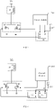
- FIG. 3 is a schematic circuit diagram of the drive circuit.
- V1 represents the drive power supply
- J1 represents the relay
- M1 represents the low-side driver unit
- Y1 represents the delay component
- R represents the first input terminal of the delay component
- B represents the second input terminal of the delay component
- Q represents the output terminal of the delay component
- V2 represents a first signal terminal of the pull-up power supply
- RT represents a first pull-up resistor.
- a level of the control signal (referred to as a control signal 1) output by the control module 203 to the first controlled terminal of the delay unit may be set based on a working principle of the delay unit, and the control signal (referred to as a control signal 2) output by the control module 203 to the second controlled terminal of the delay unit may be a constant-level signal (including a low-level signal and a high-level signal) or a pulse width modulation signal.
- the working principle of the drive circuit is as follows:
- the control module 203 When receiving a relay switch-on signal, the control module 203 outputs a high-level drive signal to the control terminal of the low-side driver unit, outputs a high-level control signal 2 to the port B of the delay component, and outputs a high-level control signal 1 to the port R of the delay component.
- a state of the port Q is a low level, and the low-side driver unit is switched on.
- the control module 203 is being reset, output of the control module 203 is in a high-impedance state, the port B of the delay component changes from a high level to a low level, and a falling edge occurs.
- the control module 203 When receiving a relay switch-off signal, the control module 203 outputs a low-level drive signal to the control terminal of the low-side driver unit, outputs a low-level control signal 2 to the port B of the delay component, and outputs a low-level control signal 1 to the port R of the delay component (a low-level control signal 1 may alternatively be first output, and then a low-level drive signal is output to the control terminal of the low-side driver unit).
- a state of the port Q is a low level, and the low-side driver unit is switched off.
- the output of the control module 203 is in a high-impedance state, and the port B of the delay component is still at a low level (no falling edge). Because there is the first pull-up unit, input of the port R changes from the low level to the high level, output of the port Q is still at the low level, the state of the low-side driver unit does not change, and the relay is not accidentally switched on.
- an output sequence of the control signal 1 and the drive signal may not be limited. If the interval between the control signal 1 and the drive signal is very long and greater than the action time of the relay, in this embodiment, the low-level control signal 1 and control signal 2 are output firstly, and then the low-level drive signal is output.
- the low-level control signal 1 is output before the low-level drive signal is output, thereby preventing the relay from being switched on and then being switched off caused by resetting of the microcontroller when the low-level control signal 1 is not sent after the low-level drive signal has been sent.
- the working principle of the drive circuit is as follows:
- the control module 203 When receiving a relay switch-on signal, the control module 203 outputs a high-level drive signal to the control terminal of the low-side driver unit, outputs a high-level control signal 1 to the port R of the delay component, and outputs a PWM control signal 2 to the port B of the delay component, so that the low-side driver unit is switched on.
- a high-level pulse is output at the port Q, which may be repeatedly triggered.
- the delay time of the delay unit is greater than a PWM period, a high level is continuously output at the port Q.
- a high level is output at the port Q of the delay module 202. It is assumed that a period of the control signal 2 is t, set delay time is T1, and T1 is greater than t, if a delay start time is between 0.5 ⁇ t and t, the time to stay at high level is [T1-0.5 ⁇ t, T1); and if a delay start time is between 0 and 0.5 ⁇ t, the time to stay at high level is T1.
- the low-side driver unit maintains an on state within the set delay time, and the relay maintains the original on state.
- the control module 203 When receiving a relay switch-off signal, the control module 203 outputs a low-level drive signal to the low-side driver unit, outputs a low-level control signal 1 to the port R of the delay component, and outputs a low-level control signal 2 to the port B of the delay component, and the low-side driver unit is switched off.
- the control module 203 When the control module 203 is being reset, the output of the control module 203 is in a high-impedance state, and the port B of the delay component is still at a low level.
- the drive circuit further includes a first anti-reverse module and a second anti-reverse module
- the delay module 202 is connected to the control terminal of the low-side driver module 201 through the first anti-reverse module
- the control module 203 is connected to the control terminal of the low-side driver module 201 through the second anti-reverse module.
- the first anti-reverse module and the second anti-reverse module are diodes. It is assumed that the load 101 is a relay and the low-side driver unit is a type-N transistor, the first level and the second level are high levels, the third level and the fourth level are low levels, and the edge signal is the falling edge signal.
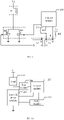
- FIG. 4 is a schematic circuit diagram of the drive circuit.
- V1 represents the drive power supply
- J1 represents the relay
- M1 represents the low-side driver unit
- Y1 represents the delay component
- R represents the first input terminal of the delay component
- B represents the second input terminal of the delay component
- Q represents the output terminal of the delay component
- V2 represents a first signal terminal of the pull-up power supply
- RT represents a first pull-up resistor
- D1 represents the first anti-reverse module
- D2 represents the second anti-reverse module.
- the control signal 2 may be a constant-level signal or a pulse width modulation signal.
- the delay module 202 is connected to the control terminal of the low-side driver module 201 through the first anti-reverse module
- the control module 203 is connected to the control terminal of the low-side driver module 201 through the second anti-reverse module, so that the drive signal from the control module 203 and the output signal from the delay module 202 compete for the power supply, and the low-side driver unit can be switched on when either signal meets the requirement.
- the drive circuit is configured to drive a load, and the load is grounded through the low-side driver module 201; and the low-side driver module 201 includes a first low-side driver unit and a second low-side driver unit, where a first terminal of the first low-side driver unit and a first terminal of the second low-side driver unit are both connected to a second terminal of the load 101, a second terminal of the first low-side driver unit and a second terminal of the second low-side driver unit are grounded, the control module 203 is connected to a control terminal of the first low-side driver unit, and an output terminal of the delay module 202 is connected to a control terminal of the second low-side driver unit.
- control module 203 may be configured to: after detecting a switch-on signal, output the drive signal of the second level or a second pulse width modulation PWM control signal to the first low-side driver unit, output a control signal of the first level or the third level to the first controlled terminal of the delay module 202, and output a control signal of a fifth level or a third pulse width modulation PWM control signal to the second controlled terminal of the delay module 202; and after detecting a switch-off signal, output the drive signal of the fourth level to the first low-side driver unit, and output a control signal of the third level to the first controlled terminal and the second controlled terminal of the delay module 202, where a period of the third pulse width modulation PWM control signal is less than the preset duration; and when the edge signal is a rising edge signal, the fifth level is a low level, or when the edge signal is a falling edge signal, the fifth level is a high level.
- the control module 203 after detecting the switch-on signal, the control module 203 outputs the first level to the first controlled terminal of the delay module 202, to ensure that when the control module 203 is being reset, the delay module 202 outputs a delay signal of the second level when the edge signal is detected at the second controlled terminal, so that the relay maintains an on state.
- FIG. 5 is a schematic circuit diagram of the drive circuit.
- V1 represents the drive power supply
- J1 represents the relay
- M1 represents the first low-side driver unit
- M2 represents the second low-side driver unit
- Y1 represents the delay component
- R represents the first input terminal of the delay component
- B represents the second input terminal of the delay component
- Q represents the output terminal of the delay component
- V2 represents a first signal terminal of the pull-up power supply
- RT represents a first pull-up resistor.
- the control signal 2 may be a constant-level signal or a pulse width modulation signal.
- control signal 2 is the constant-level signal
- the working principle of the drive circuit is as follows:
- the control module 203 When receiving a relay switch-on signal, the control module 203 outputs a PWM drive signal (second pulse width modulation PWM drive signal) to the control terminal of the first low-side driver unit, outputs a high-level control signal 1 to the port R of the delay component, and outputs a high-level control signal 2 to the port B of the delay component. Because there is no falling edge, a low level is output at the port Q of the delay component, and the first low-side driver unit is switched on. That is, when the control module 203 works normally and the relay is on, the first low-side driver unit is switched on, and in this case, the second low-side driver unit is switched off.
- PWM drive signal second pulse width modulation PWM drive signal
- the control module 203 When the control module 203 is being reset, the drive signal of the first low-side driver unit is pulled down, the control signal 2 is pulled down, and the control signal 1 is pulled up.
- the port Q of the delay component outputs a high-level pulse, so that the second low-side driver unit is switched on. In this case, the first low-side driver unit is switched off, and the relay is not switched off within the set delay time.
- the control module 203 sends a PWM drive signal, so that the first low-side driver unit is connected.
- control signal 1 is first pulled down and then pulled up, and the control signal 2 is pulled up, so that the second low-side driver unit is switched off and returns to a normal working state of the low-side driver module 201.
- the control module 203 When receiving a relay switch-off signal, the control module 203 outputs a low-level drive signal to the control terminal of the first low-side driver unit, outputs a low-level control signal 1 to the port R of the delay component, and outputs a low-level control signal 2 to the port B of the delay component. In this case, the port Q of the delay component outputs a low level, and the relay is off.
- the drive signal of the first low-side driver unit is continuously at a low level
- the control signal 1 is pulled up because of the first pull-up resistor
- the control signal 2 is continuously at a low level
- output of the port Q of the delay component is continuously at a low level
- the relay maintains an off state and is not accidentally switched on.
- the PWM drive signal is output to the first low-side driver unit, and when the control module 203 is being reset, the relay is driven through the high level instead of the PWM. Therefore, when designing the delay time (preset duration) of the delay component, a person skilled in the art may consider whether a coil of the relay can normally work within the preset duration, in order to avoid burn-down of the coil caused by a coil current that is excessively large and lasts for excessively long time when the relay is driven through a high level.
- the preset duration needs to be greater than the reset time of the control module 203, to ensure that when the control module 203 is being reset, the relay maintains a state before the control module 203 is reset; and the preset duration needs to be less than duration of high-level driving that can be tolerated by the relay, to protect the relay.
- An instruction sequence after the control module 203 completes the reset should also be considered. If delay between an instruction for controlling the first low-side driver unit and an instruction for controlling the second low-side driver unit is very long or even longer than action time of the relay, the first low-side driver unit needs to be first connected, and then the second low-side driver unit is disconnected. If the delay is very short and shorter than the action time of the relay, the sequence is not limited.
- two low-side driver units are disposed.
- the first low-side driver unit is switched on or off based on the PWM drive signal output by the control module 203
- the second low-side driver unit is switched on or off based on the delay signal output by the delay module 202, and therefore, when the control module 203 is being reset, if the relay is switched from PWM control to high-level control, a large current generated by the relay passes through the second low-side driver unit instead of the first low-side driver unit, so that a large current in the circuit does not affect service life of the first low-side driver unit, thereby ensuring safety of a vehicle during normal operation of the control module 203.
- a person skilled in the art can select a chip with a larger operating current as the second low-side driver unit.
- the delay unit includes N cascaded delay components; and first input terminals of all the delay components are mutually connected, where a joint serves as the first controlled terminal of the delay unit, a second input terminal of a 1 st delay component is connected to the second controlled terminal of the delay unit, a second input terminal of an (i+1) th delay component is connected to an output terminal of an i th delay component, and an output terminal of an N th delay component serves as the output terminal of the delay unit, where 1 ⁇ i ⁇ N, and N is an integer greater than 1.
- the delay unit is obtained by cascading a plurality of delay components, and total delay time of the delay unit is equal to a sum of delay time of the delay components, thereby prolonging the delay time.
- the delay components can have different delay time resolution. Integrating the delay components with the different delay time resolution can ensure that the delay unit can meet more delay time requirements, thereby improving delay precision. For example, when delay of 5.3 seconds is required, to improve precision, a delay component with resolution of seconds and a delay component with millisecond resolution may be selected.
- the low-side driver module 201 includes a first low-side driver unit and a second low-side driver unit, where a first terminal of the first low-side driver unit and a first terminal of the second low-side driver unit are both connected to a second terminal of the load 101, a second terminal of the first low-side driver unit and a second terminal of the second low-side driver unit are grounded, the control module 203 is connected to a control terminal of the first low-side driver unit, and the delay module 202 is connected to a control terminal of the second low-side driver unit.
- control module 203 may be configured to: after detecting a switch-on signal, output the drive signal of the second level or a second pulse width modulation PWM control signal to the first low-side driver unit, output a control signal of the first level or the third level to the first controlled terminal of the delay module 202, and output a control signal of a fifth level or a third pulse width modulation PWM control signal to the second controlled terminal of the delay module 202; and after detecting a switch-off signal, output the drive signal of the fourth level to the first low-side driver unit, and output a control signal of the third level to the first controlled terminal and the second controlled terminal of the delay module 202, where a period of the third pulse width modulation PWM control signal is less than the preset duration; and when the edge signal is a rising edge signal, the fifth level is a low level, or when the edge signal is a falling edge signal, the fifth level is a high level.
- FIG. 6 is a schematic circuit diagram of the drive circuit.
- V1 represents the drive power supply
- J1 represents the relay
- M1 represents the first low-side driver unit
- M2 represents the second low-side driver unit
- Y1 represents the first delay component
- Y2 represents the second delay component
- R represents the first input terminal
- B represents the second input terminal
- Q represents the output terminal
- P represents the joint (that is, the first controlled terminal) between the first delay component and the second delay component
- the terminal B of Y1 is the second controlled terminal
- V2 represents a first signal terminal of the pull-up power supply
- RT represents a first pull-up resistor.
- the control signal 2 may be a constant-level signal or a pulse width modulation signal.
- the control signal 2 is the PWM control signal (third pulse width modulation PWM control signal)
- the working principle of the drive circuit is as follows:
- the control module 203 When receiving a relay switch-on signal, the control module 203 outputs a PWM drive signal (second pulse width modulation PWM drive signal) to the control terminal of the first low-side driver unit, outputs a high-level control signal 1 to the port R of the first delay component and the port R of the second delay component, and outputs a PWM control signal 2 (third pulse width modulation PWM control signal) to the port B of the first delay component.
- a high level is output at the port Q of the first delay component
- a low level is output at the port Q of the second delay component
- the first low-side driver unit is switched on.
- the first low-side driver unit is conductive.
- a drive signal of the first low-side driver unit is pulled down, and the port Q of the first delay component is switched from a high level to a low level after staying at high level for a period of time, and the time to stay at high level is [T1-t/2, T1).
- the port Q of the second delay component immediately outputs a high level.
- the duration [T1-t/2, T1) the port Q of the second delay component is still at a low level.
- Total delay time of the delay module 202 is a sum of delay time of the first delay component and the second delay component, that is, (T2+T1-t/2, T2+T1).
- T1 is the delay time of the first delay component
- t is a period of the PWM control signal
- T2 is the delay time of the second delay component.
- control signal 1 is first pulled down and then pulled up, and a PWM control signal 2 is output, so that the second low-side driver unit is switched off and returns to a normal working state of the low-side driver module.
- the control module 203 When receiving a relay switch-off signal, the control module 203 outputs a low-level drive signal to the control terminal of the first low-side driver unit, so that the first low-side driver unit is switched off, and the control module outputs the low-level control signal 1 to the port R of the first delay component and the port R of the second delay component, and outputs the low-level control signal 2 to the port B of the first delay component, the port Q of the first delay component outputs a low level, a low level is output at the port Q of the second delay component, and the second low-side driver unit is switched off.
- the drive signal of the first low-side driver unit is switched to a low level, the control signal 1 is pulled up because of the first pull-up resistor, the control signal 2 is continuously at a low level, and outputs of both the port Q of the first delay component and the port Q of the second delay component are at a low level.
- the relay maintains an off state and is not accidentally switched on.
- controlling the first low-side driver unit with the PWM drive signal can adjust the on time of the low-side driver module by changing a duty ratio of the PWM drive signal, thereby adjusting a current of the load terminal.
- a plurality of delay components form the delay unit, thereby prolonging the delay time.
- the delay component is a monostable flip-flop.
- a circuit form of the delay component is not limited in this embodiment.
- FIG. 3 to FIG. 6 an example in which an edge signal is a falling edge signal is used to illustrate a circuit structure of a drive circuit.
- the edge signal may be a rising edge signal.
- FIG. 7 to FIG. 9 show a circuit structure of a drive circuit.
- V1 represents the drive power supply
- J1 represents the relay
- M1 represents the low-side driver unit
- Y1 represents the delay component
- R represents the first input terminal of the delay component
- A represents the second input terminal of the delay component
- Q represents the output terminal of the delay component
- V2 represents a first signal terminal of the pull-up power supply
- RT represents the first pull-up resistor, which constitutes the first pull-up unit
- V3 represents a second signal terminal of the pull-up power supply
- RD represents the second pull-up resistor, which constitutes the second pull-up unit.
- FIG. 9 may be implemented with reference to related descriptions of the working principle when the edge signal is the falling edge and the working principle in FIG. 7 .
- the edge signal is a rising edge signal
- the control module 203 receives a relay switch-on signal
- the control module 203 outputs a high-level drive signal and a high-level control signal 1
- the control module 203 outputs a low-level control signal 2 or a PWM control signal 2.
- the port R continuously stays at high level under action of the first pull-up unit; and the port A is changed from a low level to a high level because the output of the control module 203 is in a high-impedance state and there is a second pull-up unit.
- the control module 203 receives a relay switch-off signal, the control module 203 outputs a low-level drive signal to the control terminal of the low-side driver module 201, outputs a low-level control signal 1 to the port R of the delay component, and outputs a high-level control signal 2 to the port A of the delay component.
- the control module 203 is being reset, the port R of the delay component is pulled up, the port A of the delay component stays at high level without a rising edge, and therefore, a low level is output at the port Q of the delay component, and the relay maintains an off state.
- the delay module 202 can output a delay signal to the low-side driver module, so that the low-side driver module maintains a state before the control module 203 is reset, thereby avoiding safety hazards caused by a state change of the low-side driver module due to the reset of the control module 203.
- a third embodiment in the embodiments of this application relates to a drive circuit. This embodiment is obtained by making a further improvement on the basis of the second embodiment.
- the specific improvement is as follows: A recheck module is added to the drive circuit.
- the following uses an example to describe the recheck module.
- FIG. 10 is a schematic structural diagram of a drive circuit.
- the drive circuit is configured to drive a load 101, and the load 101 is grounded through a low-side driver module 201.
- the drive circuit also includes a recheck module 204, an input terminal of the recheck module 204 is connected to a joint between the low-side driver module 201 and the load 101, and an output terminal of the recheck module 204 is connected to the control module 203.
- the control module 203 is further configured to: at the end of the reset (work resumed), output the drive signal based on a recheck signal input by the recheck module 204 or load state data stored in a storage module, to control the low-side driver module 201.
- the following uses an example in which the load 101 is a relay to illustrate a function of the recheck module 204 and a working manner of the control module 203.
- the control module 203 can determine a drive signal based on a relay state stored in an internal register of the control module 203 (before the reset, the control module can determine a relay state based on the recheck signal input by the recheck module 204). It is assumed that the low-side driver unit is a type-N transistor, if the relay is on, the control module outputs a high-level drive signal, a high-level control signal 1, and a high-level control signal 2, to maintain the on state of the relay; and if the relay is off, the control module outputs a low-level drive signal, a low-level control signal 1, and a low-level control signal 2 to maintain the off state of the relay.
- the low-side driver unit is a type-N transistor
- the control module 203 determines a current state of the relay based on the recheck signal input by the recheck module 204. If the relay is on, the control module 203 outputs a high-level drive signal, a high-level control signal 1, and a high-level control signal 2, to maintain the on state of the relay; and if the relay is off, the control module 203 outputs a low-level drive signal, a low-level control signal 1, and a low-level control signal 2, to maintain the off state of the relay.
- the recheck module 204 includes a voltage divider sub-module and a filter sub-module, a first terminal of the voltage divider sub-module serves as the input terminal of the recheck module 204, a second terminal of the voltage divider sub-module is connected to a first terminal of the filter sub-module, and a second terminal of the filter sub-module serves as the output terminal of the recheck module 204.
- FIG. 11 is a circuit diagram of a recheck module 204.
- a voltage divider sub-module includes a first voltage divider resistor R1 and a second voltage divider resistor R2.
- a first terminal of the first voltage divider resistor R1 serves as a first terminal of the voltage divider sub-module
- a second terminal of the first voltage divider resistor R1 is connected to a first terminal of the second voltage divider resistor R2
- a second terminal of the second voltage divider resistor R2 is grounded
- a node between the second terminal of the first voltage divider resistor R1 and the first terminal of the second voltage divider resistor R2 serves as a second terminal of the voltage divider sub-module.
- the filter sub-module includes a filter resistor R3 and a filter capacitor C.
- a first terminal of the filter resistor R3 serves as a first terminal of the filter sub-module.
- a second terminal of the filter resistor R3 is connected to a first terminal of the filter capacitor C.
- a second terminal of the filter capacitor C is grounded, and a node between the second terminal of the filter resistor R3 and the first terminal of the filter capacitor C serves as a second terminal of the filter sub-module.
- FIG. 12 is a schematic circuit diagram of a drive circuit obtained after a recheck module 204 is added to the circuit structure of the delay unit shown in FIG. 4 . Meaning of each letter can be understood with reference to FIG. 4 and FIG. 11 in the second embodiment. With reference to the second embodiment 2 and FIG.
- the control module 203 when the recheck signal is at a high level, at the end of the reset (work resumed), the control module 203 outputs a high-level drive signal, a high-level control signal 1, and a high-level control signal 2, to control the relay to maintain an on state; and when the recheck signal is at a low level, at the end of the reset (work resumed), the control module 203 outputs a low-level drive signal, a low-level control signal 1 and a control signal 2, to keep the relay off.
- the recheck module 204 may alternatively use another detectable circuit form.
- a circuit structure of the recheck module 204 is not limited in this embodiment.
- FIG. 11 and FIG. 12 an example in which an input terminal of the recheck module 204 is connected to a joint between the low-side driver module 201 and the load 101 is used to illustrate a connection relationship between the recheck module 204 and another module.
- the input terminal of the recheck module 204 may alternatively be connected to a control terminal of the low-side driver module 201, and the control module 203 determines a level of the drive signal output after the reset based on an electrical signal detected by the recheck module 204.
- FIG. 11 and FIG. 12 an example in which an edge signal is a falling edge signal is used to show a connection relationship among the recheck module 204, the control module 203, the low-side driver module 201, and the delay module 202.
- the edge signal is a rising edge signal
- a connection relationship among the recheck module 204, the control module 203, the low-side driver module 201, and the delay module 202 is approximately the same as that in a case that the edge signal is the falling edge signal.
- a person skilled in the art can perform implementation with reference to FIG. 11 and FIG. 12 .
- the control module 203 determines a state of the load 101 after the reset based on the recheck signal of the recheck module 204.
- the control module 203 may alternatively output the drive signal based on load state data stored in a storage module at the end of the reset (work resumed). For example, after receiving a switch-on instruction or a switch-off instruction, the control module 203 writes a relevant instruction into the register. After the reset, the control module 203 reads the data from the register to determine the state of the load 101 after the reset. The control module 203 may alternatively determine the state of the load 101 based on the recheck signal and the load state data stored in the storage module.
- a method for the control module 203 to keep the state of the load 101 at the end of the reset (work resumed) is not limited in this embodiment.
- the delay module can output a delay signal to the low-side driver module, so that the low-side driver module maintains a state before the control module is reset, thereby avoiding safety hazards caused by a state change of the low-side driver module due to the reset of the control module.
- the control module can output a drive signal to control the low-side driver module to switch on or off, the drive signal can compete with the output signal of the delay module for power supply, and the low-side driver unit can be switched on when either signal meets the requirement.
- control module When the control module is being reset, a delay function of the entire circuit is implemented through a separate delay module, thereby simplifying drive logic of the control module and a circuit design.
- control module can directly output the control signal to the low-side driver module based on the recheck signal at the end of the reset (work resumed), so that the low-side driver module maintains the state before the reset, thereby maintaining the load in the state before the reset is completed.
- modules in the embodiments are all logical modules.
- a logical unit can be a physical unit or a part of the physical unit, or may be implemented by integrating a plurality of physical units.
- units less closely related to resolving of the technical problem mentioned in this application are not introduced, but none of this indicates that there are no other units in the embodiments.
Landscapes
- Engineering & Computer Science (AREA)
- Life Sciences & Earth Sciences (AREA)
- Sustainable Development (AREA)
- Sustainable Energy (AREA)
- Power Engineering (AREA)
- Transportation (AREA)
- Mechanical Engineering (AREA)
- Electronic Switches (AREA)
- Inverter Devices (AREA)
Applications Claiming Priority (2)
| Application Number | Priority Date | Filing Date | Title |
|---|---|---|---|
| CN202010479364.8A CN113746462B (zh) | 2020-05-29 | 2020-05-29 | 一种驱动电路 |
| PCT/CN2021/079606 WO2021238329A1 (fr) | 2020-05-29 | 2021-03-08 | Circuit d'attaque |
Publications (3)
| Publication Number | Publication Date |
|---|---|
| EP4044208A1 true EP4044208A1 (fr) | 2022-08-17 |
| EP4044208A4 EP4044208A4 (fr) | 2023-08-09 |
| EP4044208B1 EP4044208B1 (fr) | 2025-08-13 |
Family
ID=78725106
Family Applications (1)
| Application Number | Title | Priority Date | Filing Date |
|---|---|---|---|
| EP21812646.4A Active EP4044208B1 (fr) | 2020-05-29 | 2021-03-08 | Circuit d'attaque |
Country Status (4)
| Country | Link |
|---|---|
| US (2) | US12183527B2 (fr) |
| EP (1) | EP4044208B1 (fr) |
| CN (2) | CN118100889A (fr) |
| WO (1) | WO2021238329A1 (fr) |
Families Citing this family (5)
| Publication number | Priority date | Publication date | Assignee | Title |
|---|---|---|---|---|
| CN114211963B (zh) * | 2021-12-14 | 2023-10-17 | 华人运通(江苏)技术有限公司 | 一种继电器控制装置、电池管理系统及电动汽车 |
| CN114188188B (zh) * | 2021-12-20 | 2024-07-05 | 联合汽车电子有限公司 | 继电器的驱动电路 |
| CN114563967B (zh) * | 2022-02-24 | 2024-09-03 | 浙江阳光照明电器集团股份有限公司 | 一种智能插座驱动电路 |
| CN117477916B (zh) * | 2023-12-21 | 2024-03-12 | 拓尔微电子股份有限公司 | 一种低边驱动电路以及电机驱动电路 |
| CN121617857A (zh) * | 2025-11-03 | 2026-03-06 | 特百佳动力科技股份有限公司 | 继电器延时控制电路、控制方法以及车辆高压配电系统 |
Family Cites Families (17)
| Publication number | Priority date | Publication date | Assignee | Title |
|---|---|---|---|---|
| JP2010251200A (ja) * | 2009-04-17 | 2010-11-04 | Mitsuba Corp | リレー駆動回路 |
| US8013635B2 (en) * | 2010-02-11 | 2011-09-06 | Texas Instruments Incorporated | Multi-mode circuit and a method for preventing degradation in the multi-mode circuit |
| CN203456389U (zh) * | 2013-08-23 | 2014-02-26 | 艾默生电气公司 | 一种继电器驱动电路 |
| CN104057901B (zh) * | 2014-06-27 | 2016-04-27 | 深圳市金能弘盛能源科技有限公司 | 一种汽车用超级电容模组电源管理系统 |
| CN104410252B (zh) * | 2014-12-11 | 2017-09-01 | 矽力杰半导体技术(杭州)有限公司 | 源极驱动电路及其控制方法 |
| CN105609371B (zh) * | 2015-09-07 | 2017-07-07 | 南京科远驱动技术有限公司 | 一种pwm波控制的电磁继电器驱动电路及实现方法 |
| CN205149545U (zh) | 2015-10-13 | 2016-04-13 | 北京波士顿动力电池有限公司 | 一种汽车动力系统安全电路 |
| KR102121639B1 (ko) | 2016-07-15 | 2020-06-10 | 주식회사 엘지화학 | 실시간 동작 감지를 통한 컨텍터의 비정상 개방 방지 시스템 및 방법 |
| US10644689B2 (en) * | 2016-08-17 | 2020-05-05 | Denso Corporation | Transistor drive circuit and motor drive control apparatus |
| JP6684928B2 (ja) * | 2016-12-28 | 2020-04-22 | 日立オートモティブシステムズ株式会社 | 信号制御装置 |
| CN110473742B (zh) * | 2018-05-10 | 2021-07-16 | 联合汽车电子有限公司 | 高压继电器控制电路、电池管理系统及电子装置 |
| CN110262297B (zh) * | 2018-09-21 | 2020-10-02 | 宁德时代新能源科技股份有限公司 | 继电器控制装置及供电系统 |
| CN209479429U (zh) * | 2018-12-28 | 2019-10-11 | 蜂巢能源科技有限公司 | 电池管理系统电平信号控制的接触器保持电路 |
| CN209344264U (zh) | 2019-01-04 | 2019-09-03 | 蜂巢能源科技有限公司 | 电池管理系统pwm信号控制的接触器保持电路 |
| CN209232673U (zh) * | 2019-02-28 | 2019-08-09 | 杭州萤石软件有限公司 | 一种继电器控制电路 |
| CN110962602B (zh) * | 2019-04-15 | 2021-06-15 | 宁德时代新能源科技股份有限公司 | 应用于电池管理系统的负载保持电路 |
| CN210062958U (zh) * | 2019-04-24 | 2020-02-14 | 中车青岛四方机车车辆股份有限公司 | 一种紧急制动环路防抖电路、紧急制动环路和轨道车辆 |
-
2020
- 2020-05-29 CN CN202410302132.3A patent/CN118100889A/zh active Pending
- 2020-05-29 CN CN202010479364.8A patent/CN113746462B/zh active Active
-
2021
- 2021-03-08 WO PCT/CN2021/079606 patent/WO2021238329A1/fr not_active Ceased
- 2021-03-08 EP EP21812646.4A patent/EP4044208B1/fr active Active
-
2022
- 2022-05-10 US US17/740,714 patent/US12183527B2/en active Active
-
2024
- 2024-11-19 US US18/952,109 patent/US20250079099A1/en active Pending
Also Published As
| Publication number | Publication date |
|---|---|
| CN113746462A (zh) | 2021-12-03 |
| WO2021238329A1 (fr) | 2021-12-02 |
| US20220270838A1 (en) | 2022-08-25 |
| EP4044208B1 (fr) | 2025-08-13 |
| CN118100889A (zh) | 2024-05-28 |
| US12183527B2 (en) | 2024-12-31 |
| US20250079099A1 (en) | 2025-03-06 |
| EP4044208A4 (fr) | 2023-08-09 |
| CN113746462B (zh) | 2024-04-05 |
Similar Documents
| Publication | Publication Date | Title |
|---|---|---|
| US12183527B2 (en) | Drive circuit | |
| EP4043264B1 (fr) | Circuit d'attaque | |
| AU2020388721B2 (en) | Driver circuit of power conversion device and application device thereof | |
| EP0442688A2 (fr) | Circuit de commutation | |
| CN112713642B (zh) | 一种电源检测切换控制电路 | |
| CN209949004U (zh) | 电机驱动系统、电机驱动器及电动汽车 | |
| JP4792636B2 (ja) | 誘導性負荷駆動回路 | |
| JP2911453B2 (ja) | 誘導負荷を駆動するパワースイッチングトランジスタの電流再循環回路 | |
| CN116014798B (zh) | 控制电路、并联控制电路及其储能逆变器系统 | |
| CN212343647U (zh) | Mos管开关电路及其系统、电源、门锁和报警开关电路系统 | |
| CN114765361A (zh) | 一种过压保护驱动电路、电机驱动电路及车辆 | |
| CN117767222B (zh) | 直流短路保护电路 | |
| CN223024295U (zh) | 一种驱动电路、驱动芯片和变流器 | |
| CN111541217A (zh) | 短路保护电路、电器设备和电气系统 | |
| CN221610244U (zh) | 一种风扇控制电路 | |
| CN222600853U (zh) | 继电器控制电路及电子设备 | |
| US12587186B2 (en) | Switch control device and battery pack including the same | |
| EP4701029A1 (fr) | Circuit de charge pour un composant capacitif, circuit de puissance et véhicule | |
| CN117810945B (zh) | 电源反向保护电路、芯片及电子设备 | |
| CN112003242B (zh) | 一种汽车中igbt驱动电源的保护装置、方法和汽车 | |
| SU520631A1 (ru) | Устройство дл форсировки активноиндуктивной нагрузки | |
| CN119834638A (zh) | 高压集成电路、智能功率模块和电器设备 | |
| SU1457064A1 (ru) | Устройство дл питани нагрузок посто нным током на два уровн напр жени | |
| CN119675425A (zh) | 一种nmos管并联驱动电路、电池管理系统及电池包 | |
| SU1001298A1 (ru) | Самоконтролирующа с система электропитани посто нного напр жени |
Legal Events
| Date | Code | Title | Description |
|---|---|---|---|
| STAA | Information on the status of an ep patent application or granted ep patent |
Free format text: STATUS: THE INTERNATIONAL PUBLICATION HAS BEEN MADE |
|
| PUAI | Public reference made under article 153(3) epc to a published international application that has entered the european phase |
Free format text: ORIGINAL CODE: 0009012 |
|
| STAA | Information on the status of an ep patent application or granted ep patent |
Free format text: STATUS: REQUEST FOR EXAMINATION WAS MADE |
|
| 17P | Request for examination filed |
Effective date: 20220512 |
|
| AK | Designated contracting states |
Kind code of ref document: A1 Designated state(s): AL AT BE BG CH CY CZ DE DK EE ES FI FR GB GR HR HU IE IS IT LI LT LU LV MC MK MT NL NO PL PT RO RS SE SI SK SM TR |
|
| A4 | Supplementary search report drawn up and despatched |
Effective date: 20230712 |
|
| RIC1 | Information provided on ipc code assigned before grant |
Ipc: H01H 47/18 20060101AFI20230706BHEP |
|
| DAV | Request for validation of the european patent (deleted) | ||
| DAX | Request for extension of the european patent (deleted) | ||
| STAA | Information on the status of an ep patent application or granted ep patent |
Free format text: STATUS: EXAMINATION IS IN PROGRESS |
|
| 17Q | First examination report despatched |
Effective date: 20240731 |
|
| RAP1 | Party data changed (applicant data changed or rights of an application transferred) |
Owner name: CONTEMPORARY AMPEREX TECHNOLOGY(HONG KONG) LIMITED |
|
| GRAP | Despatch of communication of intention to grant a patent |
Free format text: ORIGINAL CODE: EPIDOSNIGR1 |
|
| STAA | Information on the status of an ep patent application or granted ep patent |
Free format text: STATUS: GRANT OF PATENT IS INTENDED |
|
| INTG | Intention to grant announced |
Effective date: 20250313 |
|
| GRAS | Grant fee paid |
Free format text: ORIGINAL CODE: EPIDOSNIGR3 |
|
| GRAA | (expected) grant |
Free format text: ORIGINAL CODE: 0009210 |
|
| STAA | Information on the status of an ep patent application or granted ep patent |
Free format text: STATUS: THE PATENT HAS BEEN GRANTED |
|
| AK | Designated contracting states |
Kind code of ref document: B1 Designated state(s): AL AT BE BG CH CY CZ DE DK EE ES FI FR GB GR HR HU IE IS IT LI LT LU LV MC MK MT NL NO PL PT RO RS SE SI SK SM TR |
|
| REG | Reference to a national code |
Ref country code: GB Ref legal event code: FG4D |
|
| REG | Reference to a national code |
Ref country code: CH Ref legal event code: EP |
|
| REG | Reference to a national code |
Ref country code: DE Ref legal event code: R096 Ref document number: 602021036280 Country of ref document: DE |
|
| REG | Reference to a national code |
Ref country code: IE Ref legal event code: FG4D |
|
| REG | Reference to a national code |
Ref country code: NL Ref legal event code: FP |
|
| PG25 | Lapsed in a contracting state [announced via postgrant information from national office to epo] |
Ref country code: IS Free format text: LAPSE BECAUSE OF FAILURE TO SUBMIT A TRANSLATION OF THE DESCRIPTION OR TO PAY THE FEE WITHIN THE PRESCRIBED TIME-LIMIT Effective date: 20251213 |
|
| REG | Reference to a national code |
Ref country code: LT Ref legal event code: MG9D |
|
| PG25 | Lapsed in a contracting state [announced via postgrant information from national office to epo] |
Ref country code: PT Free format text: LAPSE BECAUSE OF FAILURE TO SUBMIT A TRANSLATION OF THE DESCRIPTION OR TO PAY THE FEE WITHIN THE PRESCRIBED TIME-LIMIT Effective date: 20251215 |
|
| PG25 | Lapsed in a contracting state [announced via postgrant information from national office to epo] |
Ref country code: FI Free format text: LAPSE BECAUSE OF FAILURE TO SUBMIT A TRANSLATION OF THE DESCRIPTION OR TO PAY THE FEE WITHIN THE PRESCRIBED TIME-LIMIT Effective date: 20250813 |
|
| PG25 | Lapsed in a contracting state [announced via postgrant information from national office to epo] |
Ref country code: HR Free format text: LAPSE BECAUSE OF FAILURE TO SUBMIT A TRANSLATION OF THE DESCRIPTION OR TO PAY THE FEE WITHIN THE PRESCRIBED TIME-LIMIT Effective date: 20250813 |
|
| PG25 | Lapsed in a contracting state [announced via postgrant information from national office to epo] |
Ref country code: GR Free format text: LAPSE BECAUSE OF FAILURE TO SUBMIT A TRANSLATION OF THE DESCRIPTION OR TO PAY THE FEE WITHIN THE PRESCRIBED TIME-LIMIT Effective date: 20251114 |
|
| PG25 | Lapsed in a contracting state [announced via postgrant information from national office to epo] |
Ref country code: SE Free format text: LAPSE BECAUSE OF FAILURE TO SUBMIT A TRANSLATION OF THE DESCRIPTION OR TO PAY THE FEE WITHIN THE PRESCRIBED TIME-LIMIT Effective date: 20250813 |
|
| PG25 | Lapsed in a contracting state [announced via postgrant information from national office to epo] |
Ref country code: LV Free format text: LAPSE BECAUSE OF FAILURE TO SUBMIT A TRANSLATION OF THE DESCRIPTION OR TO PAY THE FEE WITHIN THE PRESCRIBED TIME-LIMIT Effective date: 20250813 |
|
| PG25 | Lapsed in a contracting state [announced via postgrant information from national office to epo] |
Ref country code: PL Free format text: LAPSE BECAUSE OF FAILURE TO SUBMIT A TRANSLATION OF THE DESCRIPTION OR TO PAY THE FEE WITHIN THE PRESCRIBED TIME-LIMIT Effective date: 20250813 Ref country code: BG Free format text: LAPSE BECAUSE OF FAILURE TO SUBMIT A TRANSLATION OF THE DESCRIPTION OR TO PAY THE FEE WITHIN THE PRESCRIBED TIME-LIMIT Effective date: 20250813 |
|
| PG25 | Lapsed in a contracting state [announced via postgrant information from national office to epo] |
Ref country code: RS Free format text: LAPSE BECAUSE OF FAILURE TO SUBMIT A TRANSLATION OF THE DESCRIPTION OR TO PAY THE FEE WITHIN THE PRESCRIBED TIME-LIMIT Effective date: 20251113 |
|
| PG25 | Lapsed in a contracting state [announced via postgrant information from national office to epo] |
Ref country code: ES Free format text: LAPSE BECAUSE OF FAILURE TO SUBMIT A TRANSLATION OF THE DESCRIPTION OR TO PAY THE FEE WITHIN THE PRESCRIBED TIME-LIMIT Effective date: 20250813 |
|
| REG | Reference to a national code |
Ref country code: AT Ref legal event code: MK05 Ref document number: 1825670 Country of ref document: AT Kind code of ref document: T Effective date: 20250813 |
|
| REG | Reference to a national code |
Ref country code: HU Ref legal event code: AG4A Ref document number: E073628 Country of ref document: HU |
|
| P01 | Opt-out of the competence of the unified patent court (upc) registered |
Free format text: CASE NUMBER: UPC_APP_0003267_4044208/2026 Effective date: 20260129 |
|
| PG25 | Lapsed in a contracting state [announced via postgrant information from national office to epo] |
Ref country code: SM Free format text: LAPSE BECAUSE OF FAILURE TO SUBMIT A TRANSLATION OF THE DESCRIPTION OR TO PAY THE FEE WITHIN THE PRESCRIBED TIME-LIMIT Effective date: 20250813 |
|
| PGFP | Annual fee paid to national office [announced via postgrant information from national office to epo] |
Ref country code: GB Payment date: 20260325 Year of fee payment: 6 |
|
| PG25 | Lapsed in a contracting state [announced via postgrant information from national office to epo] |
Ref country code: DK Free format text: LAPSE BECAUSE OF FAILURE TO SUBMIT A TRANSLATION OF THE DESCRIPTION OR TO PAY THE FEE WITHIN THE PRESCRIBED TIME-LIMIT Effective date: 20250813 |
|
| PGFP | Annual fee paid to national office [announced via postgrant information from national office to epo] |
Ref country code: NO Payment date: 20260324 Year of fee payment: 6 Ref country code: DE Payment date: 20260324 Year of fee payment: 6 |
|
| PG25 | Lapsed in a contracting state [announced via postgrant information from national office to epo] |
Ref country code: AT Free format text: LAPSE BECAUSE OF FAILURE TO SUBMIT A TRANSLATION OF THE DESCRIPTION OR TO PAY THE FEE WITHIN THE PRESCRIBED TIME-LIMIT Effective date: 20250813 |
|
| PG25 | Lapsed in a contracting state [announced via postgrant information from national office to epo] |
Ref country code: IT Free format text: LAPSE BECAUSE OF FAILURE TO SUBMIT A TRANSLATION OF THE DESCRIPTION OR TO PAY THE FEE WITHIN THE PRESCRIBED TIME-LIMIT Effective date: 20250813 |
|
| PGFP | Annual fee paid to national office [announced via postgrant information from national office to epo] |
Ref country code: HU Payment date: 20260316 Year of fee payment: 6 Ref country code: NL Payment date: 20260330 Year of fee payment: 6 |
|
| PGFP | Annual fee paid to national office [announced via postgrant information from national office to epo] |
Ref country code: FR Payment date: 20260330 Year of fee payment: 6 |
|
| PG25 | Lapsed in a contracting state [announced via postgrant information from national office to epo] |
Ref country code: CZ Free format text: LAPSE BECAUSE OF FAILURE TO SUBMIT A TRANSLATION OF THE DESCRIPTION OR TO PAY THE FEE WITHIN THE PRESCRIBED TIME-LIMIT Effective date: 20250813 |
|
| PG25 | Lapsed in a contracting state [announced via postgrant information from national office to epo] |
Ref country code: EE Free format text: LAPSE BECAUSE OF FAILURE TO SUBMIT A TRANSLATION OF THE DESCRIPTION OR TO PAY THE FEE WITHIN THE PRESCRIBED TIME-LIMIT Effective date: 20250813 Ref country code: SK Free format text: LAPSE BECAUSE OF FAILURE TO SUBMIT A TRANSLATION OF THE DESCRIPTION OR TO PAY THE FEE WITHIN THE PRESCRIBED TIME-LIMIT Effective date: 20250813 |
|
| REG | Reference to a national code |
Ref country code: DE Ref legal event code: R097 Ref document number: 602021036280 Country of ref document: DE |
|
| PLBE | No opposition filed within time limit |
Free format text: ORIGINAL CODE: 0009261 |
|
| STAA | Information on the status of an ep patent application or granted ep patent |
Free format text: STATUS: NO OPPOSITION FILED WITHIN TIME LIMIT |
|
| REG | Reference to a national code |
Ref country code: CH Ref legal event code: L10 Free format text: ST27 STATUS EVENT CODE: U-0-0-L10-L00 (AS PROVIDED BY THE NATIONAL OFFICE) Effective date: 20260624 |
|
| PG25 | Lapsed in a contracting state [announced via postgrant information from national office to epo] |
Ref country code: LT Free format text: LAPSE BECAUSE OF FAILURE TO SUBMIT A TRANSLATION OF THE DESCRIPTION OR TO PAY THE FEE WITHIN THE PRESCRIBED TIME-LIMIT Effective date: 20250813 |
|
| 26N | No opposition filed |
Effective date: 20260515 |