EP4044213A2 - Halbleiterbauelement und verfahren zu dessen herstellung - Google Patents
Halbleiterbauelement und verfahren zu dessen herstellung Download PDFInfo
- Publication number
- EP4044213A2 EP4044213A2 EP22166443.6A EP22166443A EP4044213A2 EP 4044213 A2 EP4044213 A2 EP 4044213A2 EP 22166443 A EP22166443 A EP 22166443A EP 4044213 A2 EP4044213 A2 EP 4044213A2
- Authority
- EP
- European Patent Office
- Prior art keywords
- semiconductor device
- layer
- anode electrode
- semiconductor layer
- sic semiconductor
- Prior art date
- Legal status (The legal status is an assumption and is not a legal conclusion. Google has not performed a legal analysis and makes no representation as to the accuracy of the status listed.)
- Withdrawn
Links
Images






Classifications
-
- H—ELECTRICITY
- H10—SEMICONDUCTOR DEVICES; ELECTRIC SOLID-STATE DEVICES NOT OTHERWISE PROVIDED FOR
- H10D—INORGANIC ELECTRIC SEMICONDUCTOR DEVICES
- H10D62/00—Semiconductor bodies, or regions thereof, of devices having potential barriers
- H10D62/80—Semiconductor bodies, or regions thereof, of devices having potential barriers characterised by the materials
- H10D62/83—Semiconductor bodies, or regions thereof, of devices having potential barriers characterised by the materials being Group IV materials, e.g. B-doped Si or undoped Ge
- H10D62/832—Semiconductor bodies, or regions thereof, of devices having potential barriers characterised by the materials being Group IV materials, e.g. B-doped Si or undoped Ge being Group IV materials comprising two or more elements, e.g. SiGe
- H10D62/8325—Silicon carbide
-
- H—ELECTRICITY
- H10—SEMICONDUCTOR DEVICES; ELECTRIC SOLID-STATE DEVICES NOT OTHERWISE PROVIDED FOR
- H10D—INORGANIC ELECTRIC SEMICONDUCTOR DEVICES
- H10D64/00—Electrodes of devices having potential barriers
- H10D64/01—Manufacture or treatment
- H10D64/012—Manufacture or treatment of electrodes comprising a Schottky barrier to a semiconductor
- H10D64/0121—Manufacture or treatment of electrodes comprising a Schottky barrier to a semiconductor to Group IV semiconductors
- H10D64/0123—Manufacture or treatment of electrodes comprising a Schottky barrier to a semiconductor to Group IV semiconductors to silicon carbide
-
- H—ELECTRICITY
- H10—SEMICONDUCTOR DEVICES; ELECTRIC SOLID-STATE DEVICES NOT OTHERWISE PROVIDED FOR
- H10D—INORGANIC ELECTRIC SEMICONDUCTOR DEVICES
- H10D64/00—Electrodes of devices having potential barriers
- H10D64/20—Electrodes characterised by their shapes, relative sizes or dispositions
- H10D64/23—Electrodes carrying the current to be rectified, amplified, oscillated or switched, e.g. sources, drains, anodes or cathodes
-
- H—ELECTRICITY
- H10—SEMICONDUCTOR DEVICES; ELECTRIC SOLID-STATE DEVICES NOT OTHERWISE PROVIDED FOR
- H10D—INORGANIC ELECTRIC SEMICONDUCTOR DEVICES
- H10D64/00—Electrodes of devices having potential barriers
- H10D64/60—Electrodes characterised by their materials
- H10D64/64—Electrodes comprising a Schottky barrier to a semiconductor
-
- H—ELECTRICITY
- H10—SEMICONDUCTOR DEVICES; ELECTRIC SOLID-STATE DEVICES NOT OTHERWISE PROVIDED FOR
- H10D—INORGANIC ELECTRIC SEMICONDUCTOR DEVICES
- H10D8/00—Diodes
- H10D8/01—Manufacture or treatment
- H10D8/051—Manufacture or treatment of Schottky diodes
-
- H—ELECTRICITY
- H10—SEMICONDUCTOR DEVICES; ELECTRIC SOLID-STATE DEVICES NOT OTHERWISE PROVIDED FOR
- H10D—INORGANIC ELECTRIC SEMICONDUCTOR DEVICES
- H10D8/00—Diodes
- H10D8/60—Schottky-barrier diodes
-
- H—ELECTRICITY
- H10—SEMICONDUCTOR DEVICES; ELECTRIC SOLID-STATE DEVICES NOT OTHERWISE PROVIDED FOR
- H10W—GENERIC PACKAGES, INTERCONNECTIONS, CONNECTORS OR OTHER CONSTRUCTIONAL DETAILS OF DEVICES COVERED BY CLASS H10
- H10W72/00—Interconnections or connectors in packages
- H10W72/50—Bond wires
- H10W72/59—Bond pads specially adapted therefor
-
- H—ELECTRICITY
- H10—SEMICONDUCTOR DEVICES; ELECTRIC SOLID-STATE DEVICES NOT OTHERWISE PROVIDED FOR
- H10W—GENERIC PACKAGES, INTERCONNECTIONS, CONNECTORS OR OTHER CONSTRUCTIONAL DETAILS OF DEVICES COVERED BY CLASS H10
- H10W72/00—Interconnections or connectors in packages
- H10W72/90—Bond pads, in general
- H10W72/921—Structures or relative sizes of bond pads
- H10W72/923—Bond pads having multiple stacked layers
-
- H—ELECTRICITY
- H10—SEMICONDUCTOR DEVICES; ELECTRIC SOLID-STATE DEVICES NOT OTHERWISE PROVIDED FOR
- H10W—GENERIC PACKAGES, INTERCONNECTIONS, CONNECTORS OR OTHER CONSTRUCTIONAL DETAILS OF DEVICES COVERED BY CLASS H10
- H10W72/00—Interconnections or connectors in packages
- H10W72/90—Bond pads, in general
- H10W72/931—Shapes of bond pads
- H10W72/932—Plan-view shape, i.e. in top view
-
- H—ELECTRICITY
- H10—SEMICONDUCTOR DEVICES; ELECTRIC SOLID-STATE DEVICES NOT OTHERWISE PROVIDED FOR
- H10W—GENERIC PACKAGES, INTERCONNECTIONS, CONNECTORS OR OTHER CONSTRUCTIONAL DETAILS OF DEVICES COVERED BY CLASS H10
- H10W72/00—Interconnections or connectors in packages
- H10W72/90—Bond pads, in general
- H10W72/931—Shapes of bond pads
- H10W72/934—Cross-sectional shape, i.e. in side view
-
- H—ELECTRICITY
- H10—SEMICONDUCTOR DEVICES; ELECTRIC SOLID-STATE DEVICES NOT OTHERWISE PROVIDED FOR
- H10W—GENERIC PACKAGES, INTERCONNECTIONS, CONNECTORS OR OTHER CONSTRUCTIONAL DETAILS OF DEVICES COVERED BY CLASS H10
- H10W72/00—Interconnections or connectors in packages
- H10W72/90—Bond pads, in general
- H10W72/941—Dispositions of bond pads
- H10W72/9415—Dispositions of bond pads relative to the surface, e.g. recessed, protruding
-
- H—ELECTRICITY
- H10—SEMICONDUCTOR DEVICES; ELECTRIC SOLID-STATE DEVICES NOT OTHERWISE PROVIDED FOR
- H10W—GENERIC PACKAGES, INTERCONNECTIONS, CONNECTORS OR OTHER CONSTRUCTIONAL DETAILS OF DEVICES COVERED BY CLASS H10
- H10W72/00—Interconnections or connectors in packages
- H10W72/90—Bond pads, in general
- H10W72/941—Dispositions of bond pads
- H10W72/944—Dispositions of multiple bond pads
-
- H—ELECTRICITY
- H10—SEMICONDUCTOR DEVICES; ELECTRIC SOLID-STATE DEVICES NOT OTHERWISE PROVIDED FOR
- H10W—GENERIC PACKAGES, INTERCONNECTIONS, CONNECTORS OR OTHER CONSTRUCTIONAL DETAILS OF DEVICES COVERED BY CLASS H10
- H10W72/00—Interconnections or connectors in packages
- H10W72/90—Bond pads, in general
- H10W72/951—Materials of bond pads
- H10W72/952—Materials of bond pads comprising metals or metalloids, e.g. PbSn, Ag or Cu
-
- H—ELECTRICITY
- H10—SEMICONDUCTOR DEVICES; ELECTRIC SOLID-STATE DEVICES NOT OTHERWISE PROVIDED FOR
- H10W—GENERIC PACKAGES, INTERCONNECTIONS, CONNECTORS OR OTHER CONSTRUCTIONAL DETAILS OF DEVICES COVERED BY CLASS H10
- H10W72/00—Interconnections or connectors in packages
- H10W72/90—Bond pads, in general
- H10W72/981—Auxiliary members, e.g. spacers
- H10W72/983—Reinforcing structures, e.g. collars
Definitions
- the present invention relates to a semiconductor device provided with a Schottky barrier diode made of SiC and a method of manufacturing the same.
- Patent Documents 1 and 2 Conventionally, attention is paid to a semiconductor power device used mainly for a system in various types of fields of power electronics such as a motor control system and a power conversion system.
- a semiconductor power device As a semiconductor power device, an SiC Schottky barrier diode is well-known (for example, Patent Documents 1 and 2).
- An object of the present invention is to provide a semiconductor device capable of reducing forward voltage while suppressing a reverse leakage current to a comparable level as in the conventional technology and decreasing a variation in the reverse leakage current, and to provide a method of manufacturing the same.
- the semiconductor device of the present invention includes a first conductive-type SiC semiconductor layer, and a Schottky metal being made of molybdenum contacting a surface of the SiC semiconductor layer and having a thickness of 10 nm to 150 nm, in which the SiC semiconductor layer has a first junction portion contacting the Schottky metal and the first junction portion is a flat structure or a structure having unevenness of 5 nm or less.
- the first junction portion of the SiC semiconductor layer to the Schottky metal is a flat structure or a structure having unevenness of 5 nm or less. This reduces forward voltage while suppressing a reverse leakage current to a comparable level as in the conventional technology.
- a thickness of the Schottky metal made of molybdenum is 10 nm to 150 nm, and thus, the stress applied to the SiC semiconductor layer from the Schottky metal can be alleviated and a variation in the stress can be decreased.
- the semiconductor device of the present invention is mass-produced, it is possible to decrease a variation in the reverse leakage current.
- the thickness of the Schottky metal is 10 nm to 100 nm, it is possible to further decrease the variation in the reverse leakage current.
- the Schottky metal has a single crystalline structure of which the crystalline interface is not exposed in a vertical cross section. According to the arrangement, it is possible to make uniform a characteristic of the entire Schottky metal.
- the semiconductor device includes an anode electrode formed on the Schottky metal, and the anode electrode includes a second junction portion made of a titanium layer contacting the Schottky metal.
- the anode electrode may include an aluminum layer formed on the titanium layer.
- the semiconductor device includes a nickel contact layer contacting a back surface of the SiC semiconductor layer.
- the semiconductor device may include a cathode electrode including a titanium layer formed on the nickel contact layer.
- an alloy layer may be further formed which contains titanium and carbon between the nickel contact layer and the cathode electrode.
- the semiconductor device may further include a carbon layer formed on the nickel contact layer.
- the semiconductor device may include a second conductive-type guard ring formed to surround the first junction portion.
- the SiC semiconductor layer may be made of n-type SiC and the guard ring may be made of p-type SiC.
- the guard ring is formed to extend outward with respect to an outer circumferential edge of the Schottky metal.
- the semiconductor device includes a field insulating film formed on a surface of the SiC semiconductor layer, the field insulating film formed therein with an opening through which the first junction portion and an inner peripheral portion of the guard ring are selectively exposed, the Schottky metal is joined to the SiC semiconductor layer within the opening and rides on the field insulating film by a riding amount of 10 ⁇ m to 60 ⁇ m from a circumferential edge of the opening.
- the Schottky metal may be formed so that an outer circumferential edge thereof contacts the guard ring.
- a method of manufacturing a semiconductor device includes a step of forming a Schottky metal made of molybdenum having a thickness of 10 nm to 150 nm, on a surface of a first conductive-type SiC semiconductor layer, and a step of performing a heat treatment on the Schottky metal in a state where the surface of the Schottky metal is exposed so that a first junction portion with the Schottky metal in the SiC semiconductor layer is made a flat structure or a structure having unevenness of 5 nm or less.
- the first junction portion of the SiC semiconductor layer to the Schottky metal is made a flat structure or a structure having unevenness of 5 nm or less . This provides a semiconductor device capable of reducing forward voltage while suppressing a reverse leakage current to a comparable level as in the conventional technology.
- a thickness of the Schottky metal made of molybdenum is 10 nm to 150 nm, and thus, the stress applied to the SiC semiconductor layer from the Schottky metal can be alleviated and a variation in the stress can be decreased.
- the semiconductor device obtained by the method is mass-produced, it is possible to decrease a variation in the reverse leakage current. As a result, it is possible to stably supply a semiconductor device having quality in which the reverse leakage current stays within a constant range.
- the step of performing a heat treatment on the SiC semiconductor layer is executed in an atmosphere where oxygen is not present. Specifically, it is preferable that the step of performing a heat treatment on the SiC semiconductor layer is executed in a nitrogen atmosphere. In that case, it is preferable that the step of performing a heat treatment on the SiC semiconductor layer is executed in a resistance heat furnace.
- the method of manufacturing a semiconductor device includes a step of forming an anode electrode on the Schottky metal, and in the step of forming the anode electrode, a titanium layer is formed so as to contact the Schottky metal.
- the step of forming the anode electrode may include a step of forming an aluminum layer so as to contact the titanium layer.
- the method of manufacturing a semiconductor device includes a step of forming a nickel contact layer on a back surface of the SiC semiconductor layer before the formation of the Schottky metal and performing a heat treatment on the nickel contact layer.
- FIG. 1 is a plan view of a semiconductor device according to a embodiment of the present invention.
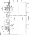
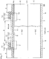
- FIG. 2 is a cross-sectional view taken along a cutting plane line II-II in FIG.1 .
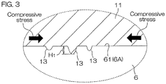
- FIG. 3 is an enlarged view of a portion within a broken line circle in FIG. 2 .
- a semiconductor device 1 includes an element in which SiC is adopted, and is of a squared chip shape in a plan view, for example.
- the semiconductor device 1 may be of a rectangular shape in a plan view.
- the size of the semiconductor device 1 has 0.5 mm to 20 mm in the respective vertical and horizontal lengths in the sheet of FIG. 1 . That is, the chip size of the semiconductor device 1 is 0.5 mm square to 20 mm square, for example.
- the surface of the semiconductor device 1 is divided by an annular guard ring 2 into an active region 3 inside the guard ring 2 and an outer circumferential region 4 outside the guard ring 2.
- the guard ring 2 is a semiconductor layer containing a p-type dopant, for example.
- B boron
- Al aluminum
- Ar argon
- the depth of the guard ring 2 may be about 100 nm to 1000 nm.
- the semiconductor device 1 includes a substrate 5 made of n + -type SiC and a drift layer 6 made of n - -type SiC laminated on a surface 5A of the substrate 5.
- the substrate 5 and the drift layer 6 are shown as one example of the SiC semiconductor layer of the present invention.
- the thickness of the substrate 5 may be 50 ⁇ m to 600 ⁇ m, and the thickness of the drift layer 6 thereon may be 3 ⁇ m to 100 ⁇ m.
- N nitrogen
- P phosphorus
- As arsenic
- the dopant concentration of the substrate 5 is relatively higher
- the dopant concentration of the drift layer 6 is relatively lower than that of the substrate 5.
- the dopant concentration of the substrate 5 may be 1 ⁇ 10 18 to 1 ⁇ 10 20 cm -3
- the dopant concentration of the drift layer 6 may be 5 ⁇ 10 14 to 5 ⁇ 10 16 cm -3 .
- a nickel (Ni) contact layer 7 is formed to cover the entire back surface 5B.
- a cathode electrode 8 is formed on the nickel contact layer 7.
- the nickel contact layer 7 is made of a nickel containing metal forming an ohmic junction with the substrate 5.
- Such a metal may include a nickel silicide layer, for example.
- a structure (Ti/Ni/Au/Ag) is formed in which titanium (Ti), nickel (Ni), gold (Au), and silver (Ag) are laminated in order from the nickel contact layer 7 side, for example, and an Ag layer is exposed to the topmost surface.
- a field insulating film 10 is formed which has a contact hole 9 through which one portion of the drift layer 6, as the active region 3, is exposed and covers the outer circumferential region 4 surrounding the active region 3.
- the field insulating film 10 maybe arranged by SiO 2 (silicon oxide), for example.
- a film thickness of the field insulating film 10 may be 0.5 ⁇ m to 3 ⁇ m.
- Schottky metal 11 and an anode electrode 12 are laminated.
- the Schottky metal 11 contacts, via the contact hole 9, the surface 6A of the drift layer 6, and forms a Schottky barrier with the drift layer 6.
- the Schottky metal 11 is made of molybdenum (Mo), and has a thickness of 10 nm to 150 nm.
- Mo molybdenum
- the Schottky metal 11 is embedded in the contact hole 9 and rides on the field insulating film 10 to cover a circumferential edge portion of the contact hole 9 in the field insulating film 10 from above. More specifically, the Schottky metal 11 preferably rides on the field insulating film 10 so that the guard ring 2 extends (projects) outward with respect to an outer circumferential edge 19 of the Schottky metal 11.
- a width W (riding amount) from a circumferential edge of the contact hole 9 of a portion that rides on the field insulating film 10 (riding portion 18) of the Schottky metal 11 to the outer circumferential edge 19 preferably is 10 ⁇ m to 60 ⁇ m.
- the circumferential edge of the contact hole 9 indicates a position at which the thickness of the field insulating film 10 is 0 (zero). Therefore, for example, when the contact hole 9 is formed in a tapered shape in which the diameter is narrower from the upper end to the lower end, the width W is measured from the lower end of the circumferential edge of the contact hole 9.
- the Schottky metal 11 is relatively thin, that is, 10 nm to 150 nm, and therefore, in the Schottky metal 11, it is possible to decrease a step between an upper portion that rides on the field insulating film 10 and a lower portion contacting the surface 6A of the drift layer 6. This decreases the step in the topmost surface of the anode electrode 12, and therefore, it is possible to easily join a bonding wire to the topmost surface.
- the Schottky metal 11 may have a single crystalline structure of which the crystalline interface is not exposed in a vertical cross section. Whether or not the Schottky metal 11 is of single crystalline structure can be confirmed by photographing and observing an image of a cross section of the Schottky metal 11 by using TEM (Transmission Electron Microscope), for example. With the arrangement, it is possible to make uniform a characteristic of the entire Schottky metal 11.
- a height H 1 of the uneven structure 13 is 5 nm or less.
- the height H 1 of the uneven structure 13 may adopt a depth at the deepest recessed portion. It is noted that the embodiment shows an example where the uneven structure 13 is formed in the junction portion 61, and the junction portion 61 of the semiconductor device 1 may be a flat structure where the unevenness is scarcely present.
- the anode electrode 12 may be of a two-layered structure including a titanium layer 121 formed on the Schottky metal 11 and an aluminum layer 122 formed on the titanium layer 121.
- the anode electrode 12 is a portion which is exposed to the topmost surface of the semiconductor device 1 and to which a bonding wire, etc., are joined. Similar to the Schottky metal 11, the anode electrode 12 rides on the field insulating film 10 to cover a circumferential edge portion of the contact hole 9 in the field insulating film 10 from above.
- the titanium layer 121 has a thickness of 70 nm to 230 nm
- the aluminum layer 122 has a thickness of 3.2 ⁇ m to 5.2 ⁇ m (4.2 ⁇ m, for example).
- the titanium layer 121 may be of a two-layered structure including a lower layer, that is, Ti, and an upper layer, that is, TiN. At this time, a thickness of Ti is 10 nm to 40 nm (25 nm, for example), and a thickness of TiN is 60 nm to 190 nm (130 nm, for example) .
- the guard ring 2 dividing the drift layer 6 into the active region 3 and the outer circumferential region 4 is formed along the profile of the contact hole 9 to cross over the inside and outside of the contact hole 9 in the field insulating film 10 (to cross over the active region 3 and the outer circumferential region 4). Therefore, the guard ring 2 has an inside portion 21 (inner peripheral portion) that projects inward of the contact hole 9 and contacts a terminal end portion of the Schottky metal 11 within the contact hole 9, and an outside portion 22 that projects outward of the contact hole 9 and faces the Schottky metal 11 with the circumferential edge portion of the field insulating film 10 being interposed therebetween.
- a surface protective film 14 is formed on the topmost surface of the semiconductor device 1.
- a surface protective film 14 is formed at a central portion of the surface protective film 14, an opening 15 is formed through which the anode electrode 12 is exposed.
- the bonding wire is joined, via the opening 15, to the anode electrode 12.
- the surface protective film 14 may be of a two-layered structure including a silicon nitride (SiN) film 141 formed on the anode electrode 12 and a polymide film 142 formed on the silicon nitride film 141.
- the silicon nitride film 141 has a thickness of 800 nm to 2400 nm (1600 nm, for example), and the polymide film 142 has a thickness of 5 ⁇ m to 14 ⁇ m (9 ⁇ m, for example).
- the semiconductor device 1 When the semiconductor device 1 is in a forward bias state where positive voltage is applied to the anode electrode 12 and negative voltage is applied to the cathode electrode 8, an electron (carrier) moves from the cathode electrode 8 to the anode electrode 12 via the active region 3 in the drift layer 6, and as a result, an electric current passes.
- the semiconductor device 1 Schottky barrier diode
- the junction portion 61 of the drift layer 6 to the Schottky metal 11 is flat or an uneven structure 13 of 5 nm or less.
- the thickness of the Schottky metal 11 made of molybdenum is 10 nm to 150 nm (100 nm, for example), and thus, the stress (compressive stress indicated by an arrow in FIG. 3 , for example) applied to the drift layer 6 from the Schottky metal 11 can be alleviated and a variation in the stress can be decreased.
- a process capability index Cpk may be 1.0 or more (preferably, 1.3 to 3.0). As a result, it is possible to stably supply the semiconductor device 1 of quality in which the reverse leakage current stays within a constant range.
- the Schottky metal 11 rides on the field insulating film 10 so that the guard ring 2 extends (projects) outward with respect to the outer circumferential edge 19 of the Schottky metal 11.
- a load connected to the semiconductor device 1 is inductive, if a current passing through the load is blocked, then counter-electromotive force is generated to the load. Resulting from the counter-electromotive force, reverse voltage in which the anode side is positive may apply between an anode and a cathode. In such a case, it is possible to relatively decrease a resistance value of the guard ring 2, and thus, it is possible to shorten a distance over which a current passes within the guard ring 2. Thus, it is possible to suppress heat generated by the current passing within the guard ring 2, and therefore, it is possible to prevent the device from thermally being destroyed. That is, it is possible to improve an inductive load resistance (L load resistance) of the semiconductor device 1.
- L load resistance inductive load resistance
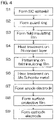
- FIG. 4 is a flowchart for describing one example of a process of manufacturing the semiconductor device 1.
- the drift layer 6 is epitaxially grown (step S1).
- a CVD (Chemical Vapor Deposition) method for example, a mask is formed on the surface 6A of the drift layer 6, and via the mask, an impurity is implanted toward the surface 6A of the drift layer 6. Thereafter, a heat treatment is performed on the drift layer 6, and the guard ring 2 is thereby formed selectively on the surface portion of the drift layer 6 (step S2).
- the field insulating film 10 that completely covers the guard ring 2 is formed on the surface 6A of the drift layer 6 (step S3).
- the nickel contact layer 7 is formed on the back surface 5B of the substrate 5.
- the substrate 5 is placed in an electric furnace, in which the nickel contact layer 7 is subjected to a heat treatment at a predetermined first temperature (step S4) . It is preferable that the heat treatment on the nickel contact layer 7 is performed in an induction heater of which the interior is adjusted to a nitrogen atmosphere, for example.
- the field insulating film 10 is patterned to form the contact hole 9, and the guard ring 2 is selectively exposed to within the contact hole 9 (step S5).
- the Schottky metal 11 made of molybdenum (Mo) having a thickness of 10 nm to 150 nm is formed. Then, the substrate 5 is placed in an electric furnace, and subjected to a heat treatment at a predetermined second temperature in a state where the surface of the Schottky metal 11 is exposed (step S6).
- the heat treatment in a state where the surface of the Schottky metal 11 is exposed means applying a heat treatment on the Schottky metal 11 when a protective cap such as metal and a film is not formed on the surface of the Schottky metal 11.
- the heat treatment on the Schottky metal 11 preferably is performed, for example, in a resistance heat furnace of which the interior is adjusted to an atmosphere where there is substantially no oxygen inside the furnace (in the embodiment, a nitrogen atmosphere). If the heat treatment is performed under a nitrogen atmosphere, then the surface portion of the Schottky metal 11 is not deteriorated into molybdenum oxide due to an oxidation of the Schottky metal 11 (molybdenum) during the heat treatment. This eliminates a need for forming a protective cap on the surface of the Schottky metal 11, and thus, it is possible to prevent the Schottky metal 11 from being raised by the thickness of the protective cap. As a result, it is possible to maintain the thickness of the Schottky metal 11 to 10 nm to 150 nm.
- step S7 the titanium layer 121 and the aluminum layer 122 are laminated in order to form the anode electrode 12 (step S7), and the surface protective film 14 is thereafter formed (step S8).
- the cathode electrode 8 is formed on the nickel contact layer 7, and the semiconductor device 1 shown in FIG. 1 , etc., is thereby obtained.
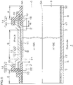
- the semiconductor device 1 may be embodied in a modified embodiment shown in FIG. 5 to FIG. 7 .
- a carbon layer 16 is formed between the nickel contact layer 7 and the cathode electrode 8.
- the carbon layer 16 is formed, during the formation of nickel silicide (nickel contact layer 7) as a result of the reaction of nickel deposited on the back surface 5B of the substrate 5 with silicon in the substrate (SiC) 5 by the heat treatment in step S4 in FIG. 4 , when redundant carbon (C) not contributing to the reaction is deposited on the surface of the nickel contact layer 7.
- an alloy layer 17 containing carbon is formed between the nickel contact layer 7 and the cathode electrode 8.
- the alloy layer 17 is formed when the carbon (C) made redundant during the formation of the above-described nickel silicide layer and titanium (Ti) of the cathode electrode 8 are alloyed as a result of an electrode material (Ti/Ni/Au/Ag) for the cathode electrode 8 being deposited and then subjected to a heat treatment, for example.
- FIG. 5 and FIG. 6 show between the nickel contact layer 7 and the cathode electrode 8, a layer resulting from the redundant carbon during the formation of the nickel silicide layer may be formed, and only one of the carbon layer 16 and the alloy layer 17 shown in each figure may be formed and both of these layers may be laminated and formed.
- the field insulating film 10 is omitted, and the entire guard ring 2 is exposed to the surface 6A of the drift layer 6.
- a terminal end portion of the Schottky metal 11 riding on the field insulating film 10 in FIG. 2 covers across the entire circumference of the inner peripheral portion of the guard ring 2 so that the guard ring 2 extends (projects) outward with respect to the outer circumferential edge 19 of the Schottky metal 11.
- the terminal end portion of the Schottky metal 11 is joined to the inner peripheral portion of the guard ring 2.
- the p-type portions may be n-type and the n-type portions may be p-type.
- the nickel contact layer 7 may be subjected to a heat treatment in a resistance heat furnace and the Schottky metal 11 may be subjected to a heat treatment in an induction heater.
- the semiconductor device (semiconductor power device) of the present invention into a power module used for an inverter circuit arranging a drive circuit for driving an electric motor utilized as a drive source for an electric vehicle (including a hybrid car), a train, and an industrial robot, etc. It is also possible to incorporate the semiconductor device of the present invention into a power module used for an inverter circuit that makes a conversion so that power generated by a solar cell, a wind power generator, other power generators (in particular, a private power generator) is coordinated with power of a commercially-available power supply.
- Example 1 20 semiconductor devices were manufactured (Comparative Example 1) in much the same way as in Example 1 except that the Schottky metal 11 was subjected to a heat treatment in the same process (oxygen atmosphere) as the nickel contact layer 7 in a state where the surface of the Schottky metal 11 (molybdenum) having a thickness of 400 nm was protected with molybdenumnitride (MoN) having a thickness of 200 nm.
- MoN molybdenumnitride
- a semiconductor device arranged to have molybdenum nitride (MoN) having a thickness of 200 nm on the Schottky metal 11 (molybdenum) having a thickness of 400 nm was manufactured (Reference Example 1) according to a flowchart in FIG. 4 .
- a Schottky interface of the semiconductor devices obtained by the Reference Example 1 and Comparative Example 1 were photographed by TEM. The obtained images are shown in FIG. 8 and FIG. 9 .
- Example 1 As shown in FIG. 8 , it was found that in the Reference Example 1, the Schottky interface (joined portion with the Schottky metal in SiC) was a smooth flat structure. It was also found that the molybdenum (Mo) was a single crystalline structure in which the crystalline interface was not exposed. It is noted that Example 1 also had a similar structure.
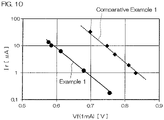
- FIG. 10 is a correlation diagram between Vf and Ir of Example 1 and Comparative Example 1, respectively.
- Example 1 As shown in FIG. 10 , it was found that in Example 1 and Comparative Example 1, there was a conflicting relationship between Vf and Ir, and when the reverse leakage current Ir was suppressed to a comparable level, Vf could be reduced in Example 1. That is, in Example 1 where the Schottky interface was flat (having a smaller amount of surface roughness), it is possible to reduce the forward voltage while suppressing the reverse leakage current to a comparable level as in Comparative Example 1.
Landscapes
- Electrodes Of Semiconductors (AREA)
- Semiconductor Integrated Circuits (AREA)
Applications Claiming Priority (4)
| Application Number | Priority Date | Filing Date | Title |
|---|---|---|---|
| JP2012129219 | 2012-06-06 | ||
| PCT/JP2013/065603 WO2013183677A1 (ja) | 2012-06-06 | 2013-06-05 | 半導体装置およびその製造方法 |
| EP19202454.5A EP3614420A1 (de) | 2012-06-06 | 2013-06-05 | Halbleiterbauelement und verfahren zu dessen herstellung |
| EP13800292.8A EP2860760A4 (de) | 2012-06-06 | 2013-06-05 | Halbleiterbauelement und verfahren zur herstellung davon |
Related Parent Applications (2)
| Application Number | Title | Priority Date | Filing Date |
|---|---|---|---|
| EP19202454.5A Division EP3614420A1 (de) | 2012-06-06 | 2013-06-05 | Halbleiterbauelement und verfahren zu dessen herstellung |
| EP13800292.8A Division EP2860760A4 (de) | 2012-06-06 | 2013-06-05 | Halbleiterbauelement und verfahren zur herstellung davon |
Publications (2)
| Publication Number | Publication Date |
|---|---|
| EP4044213A2 true EP4044213A2 (de) | 2022-08-17 |
| EP4044213A3 EP4044213A3 (de) | 2022-11-02 |
Family
ID=49712066
Family Applications (3)
| Application Number | Title | Priority Date | Filing Date |
|---|---|---|---|
| EP19202454.5A Ceased EP3614420A1 (de) | 2012-06-06 | 2013-06-05 | Halbleiterbauelement und verfahren zu dessen herstellung |
| EP22166443.6A Withdrawn EP4044213A3 (de) | 2012-06-06 | 2013-06-05 | Halbleiterbauelement und verfahren zu dessen herstellung |
| EP13800292.8A Ceased EP2860760A4 (de) | 2012-06-06 | 2013-06-05 | Halbleiterbauelement und verfahren zur herstellung davon |
Family Applications Before (1)
| Application Number | Title | Priority Date | Filing Date |
|---|---|---|---|
| EP19202454.5A Ceased EP3614420A1 (de) | 2012-06-06 | 2013-06-05 | Halbleiterbauelement und verfahren zu dessen herstellung |
Family Applications After (1)
| Application Number | Title | Priority Date | Filing Date |
|---|---|---|---|
| EP13800292.8A Ceased EP2860760A4 (de) | 2012-06-06 | 2013-06-05 | Halbleiterbauelement und verfahren zur herstellung davon |
Country Status (4)
| Country | Link |
|---|---|
| US (7) | US9799733B2 (de) |
| EP (3) | EP3614420A1 (de) |
| JP (5) | JPWO2013183677A1 (de) |
| WO (1) | WO2013183677A1 (de) |
Families Citing this family (14)
| Publication number | Priority date | Publication date | Assignee | Title |
|---|---|---|---|---|
| US9799733B2 (en) | 2012-06-06 | 2017-10-24 | Rohm Co., Ltd. | Semiconductor device having a junction portion contacting a schottky metal |
| CN106165066A (zh) * | 2014-04-09 | 2016-11-23 | 三菱电机株式会社 | 碳化硅半导体装置的制造方法及碳化硅半导体装置 |
| JP2015204333A (ja) * | 2014-04-11 | 2015-11-16 | 豊田合成株式会社 | 半導体装置および半導体装置の製造方法 |
| EP2942805B1 (de) * | 2014-05-08 | 2017-11-01 | Nexperia B.V. | Halbleiterbauelement und Herstellungsverfahren dafür |
| WO2016113004A1 (en) * | 2015-01-15 | 2016-07-21 | Abb Technology Ag | Semiconductor device including an ohmic or rectifying contact to silicon carbide and method for forming such contact |
| JP6180670B1 (ja) * | 2016-09-21 | 2017-08-16 | 新電元工業株式会社 | 半導体装置 |
| JP2018107378A (ja) * | 2016-12-28 | 2018-07-05 | 昭和電工株式会社 | 炭化珪素半導体装置とその製造方法、炭化珪素半導体の酸化膜の形成方法 |
| JP6977465B2 (ja) * | 2017-10-06 | 2021-12-08 | 株式会社デンソー | 半導体装置の製造方法 |
| JP7098906B2 (ja) * | 2017-10-11 | 2022-07-12 | 株式会社デンソー | ショットキーバリアダイオードを備えた炭化珪素半導体装置およびその製造方法 |
| JP6681935B2 (ja) * | 2018-04-16 | 2020-04-15 | 三菱電機株式会社 | 半導体装置およびその製造方法 |
| US11081555B2 (en) * | 2018-06-27 | 2021-08-03 | Ohio State Innovation Foundation | Electronic devices with ultra-high dielectric constant passivation and high mobility materials |
| JP7195086B2 (ja) * | 2018-08-29 | 2022-12-23 | 新電元工業株式会社 | 炭化ケイ素半導体装置及び炭化ケイ素半導体装置の製造方法 |
| EP4131342B1 (de) * | 2020-03-27 | 2025-02-26 | Shindengen Electric Manufacturing Co., Ltd. | Halbleiterbauelement mit breitem spalt und verfahren zur herstellung eines halbleiterbauelements mit breitem spalt |
| US20240355897A1 (en) * | 2023-04-24 | 2024-10-24 | Wolfspeed, Inc. | Semiconductor devices with low barrier height schottky contacts |
Citations (3)
| Publication number | Priority date | Publication date | Assignee | Title |
|---|---|---|---|---|
| JP2005079339A (ja) | 2003-08-29 | 2005-03-24 | National Institute Of Advanced Industrial & Technology | 半導体装置、およびその半導体装置を用いた電力変換器、駆動用インバータ、汎用インバータ、大電力高周波通信機器 |
| JP2011009797A (ja) | 2010-10-15 | 2011-01-13 | Sumitomo Electric Ind Ltd | ショットキーダイオードを有する半導体装置 |
| JP2012129219A (ja) | 2010-12-11 | 2012-07-05 | Angel Kogyo Kk | 被覆ダイオードと太陽電池モジュール用端子ボックス |
Family Cites Families (34)
| Publication number | Priority date | Publication date | Assignee | Title |
|---|---|---|---|---|
| JP3808116B2 (ja) * | 1995-04-12 | 2006-08-09 | 富士電機デバイステクノロジー株式会社 | 高耐圧ic |
| JPH09283771A (ja) * | 1996-04-12 | 1997-10-31 | Fuji Electric Co Ltd | ショットキーバリアダイオード |
| JPH10125936A (ja) | 1996-10-22 | 1998-05-15 | Rohm Co Ltd | ショットキーバリア半導体装置およびその製法 |
| WO2000021140A1 (en) * | 1998-10-08 | 2000-04-13 | Mitsubishi Denki Kabushiki Kaisha | Semiconductor device, a method of manufacturing the same, and a semiconductor device protective circuit |
| JP2003347540A (ja) * | 2002-05-23 | 2003-12-05 | Renesas Technology Corp | 半導体装置の製造方法および半導体装置 |
| US9515135B2 (en) | 2003-01-15 | 2016-12-06 | Cree, Inc. | Edge termination structures for silicon carbide devices |
| JP4724355B2 (ja) * | 2003-03-31 | 2011-07-13 | ルネサスエレクトロニクス株式会社 | 半導体装置 |
| JP4021448B2 (ja) * | 2004-03-26 | 2007-12-12 | 財団法人電力中央研究所 | ショットキー接合型半導体装置の製造方法 |
| KR100797855B1 (ko) * | 2004-03-26 | 2008-01-24 | 자이단호징 덴료쿠추오켄큐쇼 | 쇼트키 접합형 반도체 장치의 제조방법 |
| JP4087365B2 (ja) * | 2004-09-14 | 2008-05-21 | 新電元工業株式会社 | SiC半導体装置の製造方法 |
| JP3914226B2 (ja) * | 2004-09-29 | 2007-05-16 | 株式会社東芝 | 高耐圧半導体装置 |
| US7394158B2 (en) | 2004-10-21 | 2008-07-01 | Siliconix Technology C.V. | Solderable top metal for SiC device |
| JP4699812B2 (ja) | 2005-06-07 | 2011-06-15 | 株式会社デンソー | 半導体装置およびその製造方法 |
| JP5037003B2 (ja) | 2005-11-25 | 2012-09-26 | 一般財団法人電力中央研究所 | ショットキーバリアダイオードおよびその使用方法 |
| WO2008016619A1 (en) * | 2006-07-31 | 2008-02-07 | Vishay-Siliconix | Molybdenum barrier metal for sic schottky diode and process of manufacture |
| JP5078314B2 (ja) * | 2006-10-18 | 2012-11-21 | ローム株式会社 | ショットキーバリアダイオードおよびその製造方法 |
| JP2009200278A (ja) | 2008-02-22 | 2009-09-03 | Mitsubishi Electric Corp | SiCショットキバリアダイオードの製造方法 |
| JP4535151B2 (ja) | 2008-03-19 | 2010-09-01 | 株式会社デンソー | 炭化珪素半導体装置の製造方法 |
| US7851881B1 (en) * | 2008-03-21 | 2010-12-14 | Microsemi Corporation | Schottky barrier diode (SBD) and its off-shoot merged PN/Schottky diode or junction barrier Schottky (JBS) diode |
| JP2010157547A (ja) | 2008-12-26 | 2010-07-15 | Showa Denko Kk | 炭化珪素半導体素子の製造方法 |
| JP5707681B2 (ja) * | 2009-03-04 | 2015-04-30 | 富士電機株式会社 | 半導体装置およびその製造方法 |
| JP2010225914A (ja) | 2009-03-24 | 2010-10-07 | Sanyo Electric Co Ltd | ショットキーバリアダイオード |
| JP5417069B2 (ja) | 2009-07-15 | 2014-02-12 | トヨタ自動車株式会社 | 炭化ケイ素半導体装置の製造装置、製造方法 |
| JP5401356B2 (ja) * | 2010-02-09 | 2014-01-29 | 昭和電工株式会社 | 半導体装置の製造方法 |
| JP5598015B2 (ja) * | 2010-02-23 | 2014-10-01 | 株式会社デンソー | ショットキーバリアダイオードを備えた炭化珪素半導体装置およびその製造方法 |
| JP5548527B2 (ja) | 2010-06-07 | 2014-07-16 | 新電元工業株式会社 | 半導体装置の製造方法、及び半導体装置 |
| US8432000B2 (en) * | 2010-06-18 | 2013-04-30 | Fairchild Semiconductor Corporation | Trench MOS barrier schottky rectifier with a planar surface using CMP techniques |
| JP2012023199A (ja) * | 2010-07-14 | 2012-02-02 | Rohm Co Ltd | ショットキバリアダイオード |
| JP5396357B2 (ja) | 2010-09-14 | 2014-01-22 | 株式会社アマダ | レーザ加工装置及びその制御方法 |
| US9607955B2 (en) * | 2010-11-10 | 2017-03-28 | Cree, Inc. | Contact pad |
| JP5558393B2 (ja) * | 2011-03-10 | 2014-07-23 | 株式会社東芝 | 半導体装置 |
| JP2012204480A (ja) * | 2011-03-24 | 2012-10-22 | Toshiba Corp | 半導体装置及びその製造方法 |
| US8618582B2 (en) * | 2011-09-11 | 2013-12-31 | Cree, Inc. | Edge termination structure employing recesses for edge termination elements |
| US9799733B2 (en) * | 2012-06-06 | 2017-10-24 | Rohm Co., Ltd. | Semiconductor device having a junction portion contacting a schottky metal |
-
2013
- 2013-06-05 US US14/406,106 patent/US9799733B2/en active Active
- 2013-06-05 EP EP19202454.5A patent/EP3614420A1/de not_active Ceased
- 2013-06-05 JP JP2014520030A patent/JPWO2013183677A1/ja active Pending
- 2013-06-05 EP EP22166443.6A patent/EP4044213A3/de not_active Withdrawn
- 2013-06-05 WO PCT/JP2013/065603 patent/WO2013183677A1/ja not_active Ceased
- 2013-06-05 EP EP13800292.8A patent/EP2860760A4/de not_active Ceased
-
2017
- 2017-09-18 US US15/707,662 patent/US10170562B2/en active Active
- 2017-10-04 JP JP2017194448A patent/JP6685263B2/ja active Active
-
2018
- 2018-11-20 US US16/196,623 patent/US10600873B2/en active Active
-
2020
- 2020-02-10 US US16/786,686 patent/US11004939B2/en active Active
- 2020-03-31 JP JP2020062540A patent/JP6985446B2/ja active Active
-
2021
- 2021-04-12 US US17/228,189 patent/US11610970B2/en active Active
- 2021-11-25 JP JP2021191322A patent/JP2022028867A/ja active Pending
-
2023
- 2023-02-15 US US18/169,679 patent/US12057479B2/en active Active
- 2023-07-05 JP JP2023110545A patent/JP7637722B2/ja active Active
-
2024
- 2024-07-01 US US18/760,960 patent/US12543360B2/en active Active
Patent Citations (3)
| Publication number | Priority date | Publication date | Assignee | Title |
|---|---|---|---|---|
| JP2005079339A (ja) | 2003-08-29 | 2005-03-24 | National Institute Of Advanced Industrial & Technology | 半導体装置、およびその半導体装置を用いた電力変換器、駆動用インバータ、汎用インバータ、大電力高周波通信機器 |
| JP2011009797A (ja) | 2010-10-15 | 2011-01-13 | Sumitomo Electric Ind Ltd | ショットキーダイオードを有する半導体装置 |
| JP2012129219A (ja) | 2010-12-11 | 2012-07-05 | Angel Kogyo Kk | 被覆ダイオードと太陽電池モジュール用端子ボックス |
Also Published As
| Publication number | Publication date |
|---|---|
| US10170562B2 (en) | 2019-01-01 |
| JPWO2013183677A1 (ja) | 2016-02-01 |
| US20230197791A1 (en) | 2023-06-22 |
| WO2013183677A1 (ja) | 2013-12-12 |
| US20210234006A1 (en) | 2021-07-29 |
| US12543360B2 (en) | 2026-02-03 |
| EP4044213A3 (de) | 2022-11-02 |
| JP6685263B2 (ja) | 2020-04-22 |
| US20180006123A1 (en) | 2018-01-04 |
| JP7637722B2 (ja) | 2025-02-28 |
| US20190088746A1 (en) | 2019-03-21 |
| US20150129896A1 (en) | 2015-05-14 |
| US20200176572A1 (en) | 2020-06-04 |
| JP2022028867A (ja) | 2022-02-16 |
| EP2860760A4 (de) | 2016-06-15 |
| JP2023126914A (ja) | 2023-09-12 |
| US20240355886A1 (en) | 2024-10-24 |
| JP6985446B2 (ja) | 2021-12-22 |
| EP3614420A1 (de) | 2020-02-26 |
| US9799733B2 (en) | 2017-10-24 |
| US10600873B2 (en) | 2020-03-24 |
| US11610970B2 (en) | 2023-03-21 |
| JP2020127014A (ja) | 2020-08-20 |
| EP2860760A1 (de) | 2015-04-15 |
| US12057479B2 (en) | 2024-08-06 |
| JP2018050050A (ja) | 2018-03-29 |
| US11004939B2 (en) | 2021-05-11 |
Similar Documents
| Publication | Publication Date | Title |
|---|---|---|
| US12057479B2 (en) | Semiconductor device having a junction portion contacting a Schottky metal | |
| JP5525940B2 (ja) | 半導体装置および半導体装置の製造方法 | |
| JP5408929B2 (ja) | 半導体装置および半導体装置の製造方法 | |
| JP6065198B2 (ja) | 半導体装置および半導体装置の製造方法 | |
| US9177856B2 (en) | Semiconductor device and method for manufacturing same | |
| US9263527B2 (en) | Silicon carbide semiconductor device and method of manufacturing same | |
| JP2015076592A (ja) | 炭化珪素半導体装置およびその製造方法 | |
| US9583346B2 (en) | Method for manufacturing silicon carbide semiconductor device | |
| JP5999678B2 (ja) | 半導体装置および半導体装置の製造方法 | |
| JP2012174895A (ja) | 高耐圧半導体装置 | |
| JP2017017145A (ja) | 半導体装置 | |
| JP2014041920A (ja) | 半導体装置 | |
| WO2019142406A1 (ja) | 炭化珪素半導体装置 |
Legal Events
| Date | Code | Title | Description |
|---|---|---|---|
| PUAI | Public reference made under article 153(3) epc to a published international application that has entered the european phase |
Free format text: ORIGINAL CODE: 0009012 |
|
| STAA | Information on the status of an ep patent application or granted ep patent |
Free format text: STATUS: REQUEST FOR EXAMINATION WAS MADE |
|
| 17P | Request for examination filed |
Effective date: 20220404 |
|
| AC | Divisional application: reference to earlier application |
Ref document number: 2860760 Country of ref document: EP Kind code of ref document: P Ref document number: 3614420 Country of ref document: EP Kind code of ref document: P |
|
| AK | Designated contracting states |
Kind code of ref document: A2 Designated state(s): AL AT BE BG CH CY CZ DE DK EE ES FI FR GB GR HR HU IE IS IT LI LT LU LV MC MK MT NL NO PL PT RO RS SE SI SK SM TR |
|
| PUAL | Search report despatched |
Free format text: ORIGINAL CODE: 0009013 |
|
| AK | Designated contracting states |
Kind code of ref document: A3 Designated state(s): AL AT BE BG CH CY CZ DE DK EE ES FI FR GB GR HR HU IE IS IT LI LT LU LV MC MK MT NL NO PL PT RO RS SE SI SK SM TR |
|
| RIC1 | Information provided on ipc code assigned before grant |
Ipc: H01L 29/40 20060101ALN20220928BHEP Ipc: H01L 29/06 20060101ALN20220928BHEP Ipc: H01L 29/417 20060101ALI20220928BHEP Ipc: H01L 29/16 20060101ALI20220928BHEP Ipc: H01L 29/47 20060101ALI20220928BHEP Ipc: H01L 29/872 20060101ALI20220928BHEP Ipc: H01L 21/329 20060101AFI20220928BHEP |
|
| STAA | Information on the status of an ep patent application or granted ep patent |
Free format text: STATUS: EXAMINATION IS IN PROGRESS |
|
| 17Q | First examination report despatched |
Effective date: 20240305 |
|
| STAA | Information on the status of an ep patent application or granted ep patent |
Free format text: STATUS: THE APPLICATION IS DEEMED TO BE WITHDRAWN |
|
| 18D | Application deemed to be withdrawn |
Effective date: 20241029 |