EP4044263A1 - DISPOSITIF D'AFFICHAGE ET ÉLECTROLUMINESCENT À µLED À INJECTION DE PORTEUR DE CHARGE À EXTRÉMITÉ UNIQUE ET À CONTACT ÉLECTRIQUE À EXTRÉMITÉ UNIQUE, ET SON PROCÉDÉ DE PRÉPARATION - Google Patents
DISPOSITIF D'AFFICHAGE ET ÉLECTROLUMINESCENT À µLED À INJECTION DE PORTEUR DE CHARGE À EXTRÉMITÉ UNIQUE ET À CONTACT ÉLECTRIQUE À EXTRÉMITÉ UNIQUE, ET SON PROCÉDÉ DE PRÉPARATION Download PDFInfo
- Publication number
- EP4044263A1 EP4044263A1 EP20876406.8A EP20876406A EP4044263A1 EP 4044263 A1 EP4044263 A1 EP 4044263A1 EP 20876406 A EP20876406 A EP 20876406A EP 4044263 A1 EP4044263 A1 EP 4044263A1
- Authority
- EP
- European Patent Office
- Prior art keywords
- μled
- light
- emitting
- ended
- display device
- Prior art date
- Legal status (The legal status is an assumption and is not a legal conclusion. Google has not performed a legal analysis and makes no representation as to the accuracy of the status listed.)
- Granted
Links
Images

Classifications
-
- H—ELECTRICITY
- H10—SEMICONDUCTOR DEVICES; ELECTRIC SOLID-STATE DEVICES NOT OTHERWISE PROVIDED FOR
- H10H—INORGANIC LIGHT-EMITTING SEMICONDUCTOR DEVICES HAVING POTENTIAL BARRIERS
- H10H20/00—Individual inorganic light-emitting semiconductor devices having potential barriers, e.g. light-emitting diodes [LED]
- H10H20/80—Constructional details
- H10H20/85—Packages
- H10H20/857—Interconnections, e.g. lead-frames, bond wires or solder balls
-
- H—ELECTRICITY
- H10—SEMICONDUCTOR DEVICES; ELECTRIC SOLID-STATE DEVICES NOT OTHERWISE PROVIDED FOR
- H10H—INORGANIC LIGHT-EMITTING SEMICONDUCTOR DEVICES HAVING POTENTIAL BARRIERS
- H10H20/00—Individual inorganic light-emitting semiconductor devices having potential barriers, e.g. light-emitting diodes [LED]
- H10H20/80—Constructional details
- H10H20/83—Electrodes
- H10H20/831—Electrodes characterised by their shape
-
- H—ELECTRICITY
- H10—SEMICONDUCTOR DEVICES; ELECTRIC SOLID-STATE DEVICES NOT OTHERWISE PROVIDED FOR
- H10H—INORGANIC LIGHT-EMITTING SEMICONDUCTOR DEVICES HAVING POTENTIAL BARRIERS
- H10H20/00—Individual inorganic light-emitting semiconductor devices having potential barriers, e.g. light-emitting diodes [LED]
- H10H20/80—Constructional details
- H10H20/83—Electrodes
- H10H20/832—Electrodes characterised by their material
- H10H20/833—Transparent materials
-
- H—ELECTRICITY
- H10—SEMICONDUCTOR DEVICES; ELECTRIC SOLID-STATE DEVICES NOT OTHERWISE PROVIDED FOR
- H10H—INORGANIC LIGHT-EMITTING SEMICONDUCTOR DEVICES HAVING POTENTIAL BARRIERS
- H10H20/00—Individual inorganic light-emitting semiconductor devices having potential barriers, e.g. light-emitting diodes [LED]
- H10H20/80—Constructional details
- H10H20/84—Coatings, e.g. passivation layers or antireflective coatings
-
- H—ELECTRICITY
- H10—SEMICONDUCTOR DEVICES; ELECTRIC SOLID-STATE DEVICES NOT OTHERWISE PROVIDED FOR
- H10W—GENERIC PACKAGES, INTERCONNECTIONS, CONNECTORS OR OTHER CONSTRUCTIONAL DETAILS OF DEVICES COVERED BY CLASS H10
- H10W90/00—Package configurations
-
- H—ELECTRICITY
- H10—SEMICONDUCTOR DEVICES; ELECTRIC SOLID-STATE DEVICES NOT OTHERWISE PROVIDED FOR
- H10H—INORGANIC LIGHT-EMITTING SEMICONDUCTOR DEVICES HAVING POTENTIAL BARRIERS
- H10H20/00—Individual inorganic light-emitting semiconductor devices having potential barriers, e.g. light-emitting diodes [LED]
- H10H20/01—Manufacture or treatment
-
- H—ELECTRICITY
- H10—SEMICONDUCTOR DEVICES; ELECTRIC SOLID-STATE DEVICES NOT OTHERWISE PROVIDED FOR
- H10H—INORGANIC LIGHT-EMITTING SEMICONDUCTOR DEVICES HAVING POTENTIAL BARRIERS
- H10H20/00—Individual inorganic light-emitting semiconductor devices having potential barriers, e.g. light-emitting diodes [LED]
- H10H20/01—Manufacture or treatment
- H10H20/011—Manufacture or treatment of bodies, e.g. forming semiconductor layers
- H10H20/018—Bonding of wafers
-
- H—ELECTRICITY
- H10—SEMICONDUCTOR DEVICES; ELECTRIC SOLID-STATE DEVICES NOT OTHERWISE PROVIDED FOR
- H10H—INORGANIC LIGHT-EMITTING SEMICONDUCTOR DEVICES HAVING POTENTIAL BARRIERS
- H10H20/00—Individual inorganic light-emitting semiconductor devices having potential barriers, e.g. light-emitting diodes [LED]
- H10H20/01—Manufacture or treatment
- H10H20/032—Manufacture or treatment of electrodes
-
- H—ELECTRICITY
- H10—SEMICONDUCTOR DEVICES; ELECTRIC SOLID-STATE DEVICES NOT OTHERWISE PROVIDED FOR
- H10H—INORGANIC LIGHT-EMITTING SEMICONDUCTOR DEVICES HAVING POTENTIAL BARRIERS
- H10H20/00—Individual inorganic light-emitting semiconductor devices having potential barriers, e.g. light-emitting diodes [LED]
- H10H20/01—Manufacture or treatment
- H10H20/036—Manufacture or treatment of packages
- H10H20/0364—Manufacture or treatment of packages of interconnections
-
- H—ELECTRICITY
- H10—SEMICONDUCTOR DEVICES; ELECTRIC SOLID-STATE DEVICES NOT OTHERWISE PROVIDED FOR
- H10H—INORGANIC LIGHT-EMITTING SEMICONDUCTOR DEVICES HAVING POTENTIAL BARRIERS
- H10H20/00—Individual inorganic light-emitting semiconductor devices having potential barriers, e.g. light-emitting diodes [LED]
- H10H20/80—Constructional details
- H10H20/81—Bodies
- H10H20/822—Materials of the light-emitting regions
- H10H20/824—Materials of the light-emitting regions comprising only Group III-V materials, e.g. GaP
- H10H20/825—Materials of the light-emitting regions comprising only Group III-V materials, e.g. GaP containing nitrogen, e.g. GaN
Definitions
- the invention relates to the field of display and light-emitting device design, in particular to a ⁇ LED light-emitting and display device with single-ended electrical contact and single-ended carrier injection, and a manufacturing method thereof.
- ⁇ LED In the technical field of flat panel display, ⁇ LED has many advantages, and the most notable advantage is low power consumption, high brightness, ultra-high definition, high color saturation, higher response speed, longer service life and higher work efficiency and the like. It is a new transformational display technology and is expected to replace almost all applications of TFT liquid crystal display in the field of flat panel display.
- the current ⁇ LED production process follows a traditional LED manufacturing method, in which a pn junction grows on the base surface by various thin film growth methods and then is cut into micro-sized LED ⁇ LED chips.
- the ⁇ LED chips are transferred to a circuit substrate by various mechanical tools, and the accurate electrical contact between the ⁇ LED chips and a driving electrode needs to be achieved through accurate alignment and bonding, so the device manufacturing efficiency is low and the yield is low.
- the purpose of the present invention is to propose a ⁇ LED light-emitting and display device with single-ended electrical contact and single-ended carrier injection and a manufacturing method of the ⁇ LED light-emitting and display device, which avoids the complicated bonding process and is expected to improve the market competitiveness of the ⁇ LED light-emitting and display device.
- a ⁇ LED light-emitting and display device with single-ended electrical contact and single-ended carrier injection comprises more than one pixel unit, and each pixel unit sequentially comprises a lower pixel electrode, ⁇ LED chips, an insulating layer, and an upper pixel electrode from bottom to top, wherein the ⁇ LED chips directly contact with the lower pixel electrode, external carriers are injected into the ⁇ LED chips through the lower pixel electrode, the insulating layer prevents the external carriers from being injected into the ⁇ LED chips through the upper pixel electrode, and the ⁇ LED chips are lit by an alternating electric field applied between the upper pixel electrode and the lower pixel electrode.
- the ⁇ LED chips comprise a P-type semiconductor layer, a light-emitting layer and a N-type semiconductor layer, and the P-type semiconductor layer, the light-emitting layer and the N-type semiconductor layer are stacked to form a semiconductor junction capable of emitting light under the action of an electric field.
- the semiconductor junction in the ⁇ LED chips comprises a single PN junction, a single heterojunction, a composite PN junction comprising a plurality of PN junctions, or a combined semiconductor junction comprising a PN junction and a heterojunction.
- the semiconductor junction is located on the surface or in the inside of the ⁇ LED chips.
- the p-type semiconductor layer has a thickness of 1 nm-2.0 ⁇ m
- the light-emitting layer has a thickness of 1 nm-1.0 ⁇ m
- the n-type semiconductor layer has a thickness of 1 nm-2.5 ⁇ m.
- one or more than two ⁇ LED chip are present in each pixel unit.
- the size of the upper pixel electrode or the lower pixel electrode in a pixel unit is not smaller than the sum of the sizes of all the ⁇ LED chips in the pixel unit.
- the ⁇ LED chips have a size of 1 nm to 1000 ⁇ m and a thickness of 1 nm to 100 ⁇ m.
- At least one of the upper pixel electrode and the lower pixel electrode is a transparent electrode, so that the two sides of the device can be completely transparent, or one side of the device is transparent and the other side of the device is non-transparent, wherein the material of the transparent electrode comprises graphene, indium tin oxide, carbon nanotubes, silver nanowires, copper nanowires or a combination thereof, and the material of a non-transparent electrode comprises gold, silver, aluminum, copper or a combination thereof.
- the material of the insulating layer has a light transmittance of greater than or equal to 80% in a visible light range, and the material is an organic insulating material, an inorganic insulating material, air or a combination thereof.
- the insulating layer has a thickness of 1 nm to 1000 ⁇ m.
- the waveform of the alternating electric field comprises sine wave, triangle wave, square wave, pulse or a combination thereof.
- the alternating electric field has a frequency of 1 Hz to 1000 M Hz.
- the ⁇ LED chips emit light (comprising infrared light or ultraviolet light) of different colors by selecting different semiconductor materials.
- the ⁇ LED chips can emit light of the same color or light of different mixed colors by using a composite PN junction or a combined semiconductor junction.
- the ⁇ LED light-emitting and display device is prepared on a rigid material comprising glass, ceramics and sapphire or prepared on a flexible material comprising PI.
- the present invention also provides a manufacturing method of a ⁇ LED light-emitting and display device with single-ended electrical contact and single-ended carrier injection, comprising the following steps:
- the operation of the ⁇ LED device is achieved by applying an AC driving signal to the upper pixel electrode array and the lower pixel electrode array.
- S2 specifically comprises: arranging ⁇ LED chips emitting light of different colors on the surface of the base plate of the substrate by means of inkjet printing, silk-screen printing, spin coating, brush coating, roll coating, chemical self-assembly, electromagnetic self-assembly and the like.
- S2 specifically comprises: disposing a patterned ⁇ LED array on the surface of the base plate of the substrate using an in-situ growth method.
- the present invention has the following beneficial effects: the ⁇ LED of the present invention utilizes electron-hole recombination to generate radiative transition, only single-ended electrical contact exists between the n-type semiconductor layer and p-type semiconductor layer of the ⁇ LED chips of the present invention and the external driving electrode and no bonding is required, which differs from a traditional ⁇ LED device. Therefore, the ⁇ LED device proposed by the present invention avoids the complicated bonding process, can shorten the manufacturing cycle of the ⁇ LED light-emitting and display screen and improve the yield, and is expected to greatly improve the market competitiveness of the ⁇ LED.
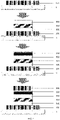
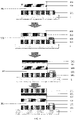
- 1 is the lower base plate
- 101 is the patterned lower pixel electrode arranged on the surface of the lower base plate
- 102 is the injection electrode
- 2 is the upper base plate
- 201 is the patterned upper pixel electrode arranged on the surface of the upper base plate
- 202 is the insulating layer
- 3 is the ⁇ LED chips
- 301 is the P-type semiconductor layer
- 302 is the N-type semiconductor layer
- 303 and 304 are light-emitting layers
- 305 is the P-type semiconductor layer.
- the present embodiment provides a ⁇ LED light-emitting and display device with single-ended electrical contact and single-ended carrier injection comprising more than one pixel unit, and each pixel unit sequentially comprises a lower pixel electrode, ⁇ LED chips, an insulating layer, and an upper pixel electrode from bottom to top, wherein the ⁇ LED chips directly contact with the lower pixel electrode, external carriers are injected into the ⁇ LED chips through the lower pixel electrode, the insulating layer prevents the external carriers from being injected into the ⁇ LED chips through the upper pixel electrode, and the ⁇ LED chips are lit by an alternating electric field applied between the upper pixel electrode and the lower pixel electrode.
- the ⁇ LED chips comprise a P-type semiconductor layer, a light-emitting layer and a N-type semiconductor layer, and the P-type semiconductor layer, the light-emitting layer and the N-type semiconductor layer are stacked to form a semiconductor junction capable of emitting light under the action of an electric field.
- the semiconductor junction in the ⁇ LED chips comprises a single PN junction, a single heterojunction, a composite PN junction comprising a plurality of PN junctions, or a combined semiconductor junction comprising a PN junction and a heteroj unction.
- the semiconductor junction is located on the surface or in the inside of the ⁇ LED chips.
- the p-type semiconductor layer has a thickness of 1 nm-2.0 ⁇ m
- the light-emitting layer has a thickness of 1 nm-1.0 ⁇ m
- the n-type semiconductor layer has a thickness of 1 nm-2.5 ⁇ m.
- one or more than two chips are present in each pixel unit.
- the size of the upper pixel electrode or the lower pixel electrode in a pixel unit is not smaller than the sum of the sizes of all the ⁇ LED chips in the pixel unit.
- the ⁇ LED chips have a size of 1 nm to 1000 ⁇ m and a thickness of 1 nm to 100 ⁇ m.
- At least one of the upper pixel electrode and the lower pixel electrode is a transparent electrode, so that the two sides of the device can be completely transparent, or one side of the device is transparent and the other side of the device is non-transparent,
- the material of the transparent electrode comprises graphene, indium tin oxide, carbon nanotubes, silver nanowires, copper nanowires or a combination thereof
- the material of a non-transparent electrode comprises gold, silver, aluminum, copper or a combination thereof.
- the material of the insulating layer has a light transmittance of greater than or equal to 80% in a visible light range, and the material is an organic insulating material, an inorganic insulating material, air or a combination thereof.
- the insulating layer has a thickness of 1 nm to 1000 ⁇ m.
- the waveform of the alternating electric field comprises sine wave, triangle wave, square wave, pulse or a combination thereof.
- the alternating electric field has a frequency of 1 Hz to 1000 M Hz.
- the ⁇ LED chips emit light (comprising infrared light or ultraviolet light) of different colors by selecting different semiconductor materials.
- the ⁇ LED chips can emit light of the same color or light of different mixed colors by using a composite PN junction or a combined semiconductor junction.
- the ⁇ LED light-emitting and display device is prepared on a rigid material comprising glass, ceramics and sapphire or prepared on a flexible material comprising PI.
- FIG. 1 is a cross-section schematic diagram of a first pixel unit structure according to the present embodiment, wherein the ⁇ LED chips have a single semiconductor junction with a structure of p-type semiconductor material-multiple quantum well-n-type semiconductor material.
- the ⁇ LED3, e.g., a GaN-based LED formed by an epitaxial method, comprises a N-type doped GaN layer 302, a P-doped GaN layer 301 and a multiple-quantum-well light-emitting layer 303.
- the ⁇ LED3 has a plane size of 20 ⁇ m ⁇ 20 ⁇ m.
- the ⁇ LED3 is arranged on the surface of the lower pixel electrode 101, the insulating layer 202 is arranged on the surface of the ⁇ LED3, the upper pixel electrode 201 is arranged on the surface of the insulating layer 202, the upper pixel electrode is indium tin oxide, and the sizes of the lower pixel electrode 101 and the upper pixel electrode 201 are both 60 ⁇ m ⁇ 60 ⁇ m.
- the insulating layer 202 has a thickness of 100 nm, and the insulating layer 202 is aluminum oxide.
- the ⁇ LED3 When an alternating current signal is applied between the lower pixel electrode 101 and the upper pixel electrode 201, the ⁇ LED3 can emit light.
- FIG. 2 is a cross-section schematic diagram of a second pixel unit structure according to the present embodiment.
- the ⁇ LED chips have a compound semiconductor junction with a structure of p-type semiconductor material-multiple quantum well-n-type semiconductor material-multiple quantum well-p-type semiconductor material.
- the ⁇ LED3 has a plane size of 20 ⁇ m ⁇ 20 ⁇ m.
- the ⁇ LED3 is arranged on the surface of the lower pixel electrode 101, the insulating layer 202 is arranged on the surface of the ⁇ LED3, the upper pixel electrode 201 is arranged on the surface of the insulating layer 202, the upper pixel electrode is indium tin oxide, and the sizes of the lower pixel electrode 101 and the upper pixel electrode 201 are both 60 ⁇ m ⁇ 60 ⁇ m.
- the insulating layer 202 has a thickness of 100 nm, and the insulating layer 202 is aluminum oxide.
- the ⁇ LED3 When an alternating current signal is applied between the lower pixel electrode 101 and the upper pixel electrode 201, the ⁇ LED3 can emit light.
- the present embodiment also provides a manufacturing method of a ⁇ LED light-emitting and display device with single-ended electrical contact and single-ended carrier injection, comprising the following steps:
- the operation of the ⁇ LED device is achieved by applying an AC driving signal to the upper pixel electrode array and the lower pixel electrode array.
- S2 specifically comprises: arranging ⁇ LED chips emitting light of different colors on the surface of the base plate of the substrate by means of inkjet printing, silk-screen printing, spin coating, brush coating, roll coating, chemical self-assembly, electromagnetic self-assembly and the like.
- S2 specifically comprises: disposing a patterned ⁇ LED chip array on the surface of the base plate of the substrate using an in-situ growth method.
- FIG. 3 shows a device manufacturing method using the pixel unit of FIG. 1 , wherein the ⁇ LED chips of the ⁇ LED light-emitting and display device are arranged on the surface of the lower base plate 1 by means of a transfer method, and the manufacturing method comprises the following steps:
- the present embodiment also provides another ⁇ LED light-emitting and display device with single-ended electrical contact and single-ended carrier injection, wherein the ⁇ LED chips are grown on the surface of the lower base plate 1 in situ, and the material of the lower base plate can be but not limited to sapphire, silicon, etc., wherein the ⁇ LED3 ⁇ LED chips are leaked out of a n-type GaN mesa, and the n-type GaN serves as the lower pixel electrode 101.
- the manufacturing method specifically comprises the following steps:
Landscapes
- Electroluminescent Light Sources (AREA)
- Led Devices (AREA)
Applications Claiming Priority (2)
| Application Number | Priority Date | Filing Date | Title |
|---|---|---|---|
| CN201910984757.1A CN110690329B (zh) | 2019-10-16 | 2019-10-16 | 一种单端电学接触、单端载流子注入的μLED发光与显示器件及其制备方法 |
| PCT/CN2020/112400 WO2021073286A1 (fr) | 2019-10-16 | 2020-08-31 | DISPOSITIF D'AFFICHAGE ET ÉLECTROLUMINESCENT À μLED À INJECTION DE PORTEUR DE CHARGE À EXTRÉMITÉ UNIQUE ET À CONTACT ÉLECTRIQUE À EXTRÉMITÉ UNIQUE, ET SON PROCÉDÉ DE PRÉPARATION |
Publications (3)
| Publication Number | Publication Date |
|---|---|
| EP4044263A1 true EP4044263A1 (fr) | 2022-08-17 |
| EP4044263A4 EP4044263A4 (fr) | 2022-12-28 |
| EP4044263B1 EP4044263B1 (fr) | 2026-05-06 |
Family
ID=69112981
Family Applications (1)
| Application Number | Title | Priority Date | Filing Date |
|---|---|---|---|
| EP20876406.8A Active EP4044263B1 (fr) | 2019-10-16 | 2020-08-31 | PROCÉDÉ DE FABRICATION D'UN DISPOSITIF À µLED ÉLECTROLUMINESCENT ET D'AFFICHAGE, À CONTACT ÉLECTRIQUE À EXTRÉMITÉ UNIQUE ET À INJECTION DE PORTEUR DE CHARGE À EXTRÉMITÉ UNIQUE |
Country Status (4)
| Country | Link |
|---|---|
| US (1) | US12268040B2 (fr) |
| EP (1) | EP4044263B1 (fr) |
| CN (1) | CN110690329B (fr) |
| WO (1) | WO2021073286A1 (fr) |
Families Citing this family (3)
| Publication number | Priority date | Publication date | Assignee | Title |
|---|---|---|---|---|
| CN110690329B (zh) * | 2019-10-16 | 2021-06-29 | 福州大学 | 一种单端电学接触、单端载流子注入的μLED发光与显示器件及其制备方法 |
| CN116543690A (zh) * | 2023-05-19 | 2023-08-04 | 福州大学 | 一种基于感生电场的微型发光器件的像素结构及驱动方法 |
| CN118135945B (zh) * | 2024-04-25 | 2025-10-21 | 福州大学 | 一种单端注入型发光器件的灰度调制方法 |
Family Cites Families (11)
| Publication number | Priority date | Publication date | Assignee | Title |
|---|---|---|---|---|
| JPH03187189A (ja) * | 1989-12-15 | 1991-08-15 | Nippon Telegr & Teleph Corp <Ntt> | 固体光源 |
| JPH11339967A (ja) * | 1998-05-25 | 1999-12-10 | Tdk Corp | 有機el素子 |
| KR20010010228A (ko) * | 1999-07-16 | 2001-02-05 | 김순택 | 교류 전계 발광소자 및 구동방법 |
| CN101639175A (zh) * | 2009-09-04 | 2010-02-03 | 詹英英 | 交流led发光对管 |
| US8957442B2 (en) * | 2011-02-11 | 2015-02-17 | Semiconductor Energy Laboratory Co., Ltd. | Light-emitting device and display device |
| JP6419089B2 (ja) * | 2013-02-28 | 2018-11-07 | フィリップス ライティング ホールディング ビー ヴィ | 容量性駆動に適したシンプルなledパッケージ |
| KR101436123B1 (ko) * | 2013-07-09 | 2014-11-03 | 피에스아이 주식회사 | 초소형 led를 포함하는 디스플레이 및 이의 제조방법 |
| CN104465921B (zh) * | 2014-12-24 | 2017-06-20 | 中国科学院半导体研究所 | 电容式结构的发光二极管集成芯片及其制备方法 |
| US11600743B2 (en) * | 2017-03-30 | 2023-03-07 | Vuereal Inc. | High efficient microdevices |
| US10989755B2 (en) * | 2017-06-20 | 2021-04-27 | Apple Inc. | Light emitting diode (LED) test apparatus and method of manufacture |
| CN110690329B (zh) * | 2019-10-16 | 2021-06-29 | 福州大学 | 一种单端电学接触、单端载流子注入的μLED发光与显示器件及其制备方法 |
-
2019
- 2019-10-16 CN CN201910984757.1A patent/CN110690329B/zh active Active
-
2020
- 2020-08-31 EP EP20876406.8A patent/EP4044263B1/fr active Active
- 2020-08-31 US US17/768,483 patent/US12268040B2/en active Active
- 2020-08-31 WO PCT/CN2020/112400 patent/WO2021073286A1/fr not_active Ceased
Also Published As
| Publication number | Publication date |
|---|---|
| WO2021073286A1 (fr) | 2021-04-22 |
| US12268040B2 (en) | 2025-04-01 |
| CN110690329B (zh) | 2021-06-29 |
| US20240297281A1 (en) | 2024-09-05 |
| CN110690329A (zh) | 2020-01-14 |
| EP4044263B1 (fr) | 2026-05-06 |
| EP4044263A4 (fr) | 2022-12-28 |
Similar Documents
| Publication | Publication Date | Title |
|---|---|---|
| CN107393940B (zh) | Led显示设备及其制造方法 | |
| CN110676284B (zh) | 一种非电学接触、无外部载流子注入的μLED发光与显示器件 | |
| CN110676250B (zh) | 一种无电学接触无巨量转移的全彩化μLED显示器件 | |
| US11211366B2 (en) | Method for manufacturing display device and substrate for manufacturing display device | |
| CN110676282B (zh) | 一种无电学接触的全彩化μLED微显示器件及其制造方法 | |
| EP4044265B1 (fr) | Dispositif d'affichage électroluminescent à ndel ordonné à orientation à contact électrique non direct | |
| CN109417082A (zh) | 半导体器件以及包括半导体器件的显示装置 | |
| US12268040B2 (en) | μLED light-emitting and display device with single-ended electrical contact and single-ended carrier injection, and manufacturing method therefor | |
| KR102078643B1 (ko) | 원칩 타입의 발광 다이오드를 이용한 디스플레이 장치 및 그 제조 방법 | |
| CN114975699A (zh) | 一种全彩氮化物半导体Micro-LED阵列的单片集成制备方法 | |
| CN110265587A (zh) | 显示面板及其制造方法 | |
| CN110556459A (zh) | 一种彩色μLED发光显示器件 | |
| CN110311053A (zh) | 显示面板及其制造方法 | |
| CN110690328B (zh) | 一种基于波长下转换的无电学接触μLED发光器件 | |
| US20230031398A1 (en) | Display device using semiconductor light-emitting element, and manufacturing method therefor | |
| US20230078258A1 (en) | Display device using semiconductor light-emitting element, and method for manufacturing same | |
| CN111863871A (zh) | 一种显示面板及其制备方法 | |
| CN115084333A (zh) | 一种倒装式GaN基Micro-LED显示模组及其制备方法 | |
| US20230327062A1 (en) | Semiconductor light-emitting device and display device using semiconductor light-emitting device | |
| CN209929308U (zh) | 显示面板 | |
| CN113629095A (zh) | 发光显示装置以及发光显示装置的制作方法 | |
| CN113270441B (zh) | Led芯片结构及其制备方法、显示模组以及电子设备 | |
| US20240072213A1 (en) | Display device using semiconductor light-emitting elements | |
| CN118338730B (zh) | 一种Micro-LED和QLED混合全彩显示器件单片集成结构及其制备方法 | |
| KR102375861B1 (ko) | 백투백 구조의 초소형 이중 led 소자 및 그 제조 방법과 백투백 구조의 초소형 이중 led 의 전극 어셈블리 및 그 제조방법 |
Legal Events
| Date | Code | Title | Description |
|---|---|---|---|
| STAA | Information on the status of an ep patent application or granted ep patent |
Free format text: STATUS: THE INTERNATIONAL PUBLICATION HAS BEEN MADE |
|
| PUAI | Public reference made under article 153(3) epc to a published international application that has entered the european phase |
Free format text: ORIGINAL CODE: 0009012 |
|
| STAA | Information on the status of an ep patent application or granted ep patent |
Free format text: STATUS: REQUEST FOR EXAMINATION WAS MADE |
|
| 17P | Request for examination filed |
Effective date: 20220513 |
|
| AK | Designated contracting states |
Kind code of ref document: A1 Designated state(s): AL AT BE BG CH CY CZ DE DK EE ES FI FR GB GR HR HU IE IS IT LI LT LU LV MC MK MT NL NO PL PT RO RS SE SI SK SM TR |
|
| A4 | Supplementary search report drawn up and despatched |
Effective date: 20221130 |
|
| RIC1 | Information provided on ipc code assigned before grant |
Ipc: H01L 33/32 20100101ALN20221124BHEP Ipc: H01L 33/44 20100101ALI20221124BHEP Ipc: H01L 33/42 20100101ALI20221124BHEP Ipc: H01L 33/00 20100101ALI20221124BHEP Ipc: H01L 33/38 20100101ALI20221124BHEP Ipc: H01L 25/075 20060101AFI20221124BHEP |
|
| DAV | Request for validation of the european patent (deleted) | ||
| DAX | Request for extension of the european patent (deleted) | ||
| REG | Reference to a national code |
Ref country code: DE Ref legal event code: R079 Free format text: PREVIOUS MAIN CLASS: H01L0033380000 Ipc: H10H0029300000 Ref country code: DE Ref legal event code: R079 Ref document number: 602020071860 Country of ref document: DE Free format text: PREVIOUS MAIN CLASS: H01L0033380000 Ipc: H10H0029300000 |
|
| GRAP | Despatch of communication of intention to grant a patent |
Free format text: ORIGINAL CODE: EPIDOSNIGR1 |
|
| STAA | Information on the status of an ep patent application or granted ep patent |
Free format text: STATUS: GRANT OF PATENT IS INTENDED |
|
| RIC1 | Information provided on ipc code assigned before grant |
Ipc: H10H 29/30 20250101AFI20260204BHEP Ipc: H10H 20/831 20250101ALI20260204BHEP Ipc: H10H 20/833 20250101ALI20260204BHEP Ipc: H10H 20/84 20250101ALI20260204BHEP Ipc: H10H 29/01 20250101ALI20260204BHEP Ipc: H10W 90/00 20260101ALI20260204BHEP Ipc: H10H 20/825 20250101ALN20260204BHEP |
|
| INTG | Intention to grant announced |
Effective date: 20260216 |
|
| GRAS | Grant fee paid |
Free format text: ORIGINAL CODE: EPIDOSNIGR3 |
|
| GRAA | (expected) grant |
Free format text: ORIGINAL CODE: 0009210 |
|
| STAA | Information on the status of an ep patent application or granted ep patent |
Free format text: STATUS: THE PATENT HAS BEEN GRANTED |
|
| AK | Designated contracting states |
Kind code of ref document: B1 Designated state(s): AL AT BE BG CH CY CZ DE DK EE ES FI FR GB GR HR HU IE IS IT LI LT LU LV MC MK MT NL NO PL PT RO RS SE SI SK SM TR |
|
| REG | Reference to a national code |
Ref country code: CH Ref legal event code: F10 Free format text: ST27 STATUS EVENT CODE: U-0-0-F10-F00 (AS PROVIDED BY THE NATIONAL OFFICE) Effective date: 20260506 Ref country code: GB Ref legal event code: FG4D |
|
| REG | Reference to a national code |
Ref country code: DE Ref legal event code: R096 Ref document number: 602020071860 Country of ref document: DE |
|
| REG | Reference to a national code |
Ref country code: IE Ref legal event code: FG4D |