EP4044574A1 - Elektronische vorrichtung - Google Patents
Elektronische vorrichtung Download PDFInfo
- Publication number
- EP4044574A1 EP4044574A1 EP20874260.1A EP20874260A EP4044574A1 EP 4044574 A1 EP4044574 A1 EP 4044574A1 EP 20874260 A EP20874260 A EP 20874260A EP 4044574 A1 EP4044574 A1 EP 4044574A1
- Authority
- EP
- European Patent Office
- Prior art keywords
- unit
- photoelectric conversion
- electronic apparatus
- conversion units
- light
- Prior art date
- Legal status (The legal status is an assumption and is not a legal conclusion. Google has not performed a legal analysis and makes no representation as to the accuracy of the status listed.)
- Withdrawn
Links
Images











Classifications
-
- H—ELECTRICITY
- H04—ELECTRIC COMMUNICATION TECHNIQUE
- H04N—PICTORIAL COMMUNICATION, e.g. TELEVISION
- H04N7/00—Television systems
- H04N7/14—Systems for two-way working
- H04N7/141—Systems for two-way working between two video terminals, e.g. videophone
- H04N7/142—Constructional details of the terminal equipment, e.g. arrangements of the camera and the display
- H04N7/144—Constructional details of the terminal equipment, e.g. arrangements of the camera and the display camera and display on the same optical axis, e.g. optically multiplexing the camera and display for eye to eye contact
-
- H—ELECTRICITY
- H04—ELECTRIC COMMUNICATION TECHNIQUE
- H04M—TELEPHONIC COMMUNICATION
- H04M1/00—Substation equipment, e.g. for use by subscribers
- H04M1/02—Constructional features of telephone sets
- H04M1/0202—Portable telephone sets, e.g. cordless phones, mobile phones or bar type handsets
- H04M1/026—Details of the structure or mounting of specific components
- H04M1/0264—Details of the structure or mounting of specific components for a camera module assembly
-
- G—PHYSICS
- G02—OPTICS
- G02B—OPTICAL ELEMENTS, SYSTEMS OR APPARATUS
- G02B27/00—Optical systems or apparatus not provided for by any of the groups G02B1/00 - G02B26/00, G02B30/00
- G02B27/28—Optical systems or apparatus not provided for by any of the groups G02B1/00 - G02B26/00, G02B30/00 for polarising
- G02B27/288—Filters employing polarising elements, e.g. Lyot or Solc filters
-
- G—PHYSICS
- G02—OPTICS
- G02B—OPTICAL ELEMENTS, SYSTEMS OR APPARATUS
- G02B5/00—Optical elements other than lenses
- G02B5/30—Polarising elements
- G02B5/3025—Polarisers, i.e. arrangements capable of producing a definite output polarisation state from an unpolarised input state
-
- G—PHYSICS
- G02—OPTICS
- G02B—OPTICAL ELEMENTS, SYSTEMS OR APPARATUS
- G02B5/00—Optical elements other than lenses
- G02B5/30—Polarising elements
- G02B5/3025—Polarisers, i.e. arrangements capable of producing a definite output polarisation state from an unpolarised input state
- G02B5/3058—Polarisers, i.e. arrangements capable of producing a definite output polarisation state from an unpolarised input state comprising electrically conductive elements, e.g. wire grids, conductive particles
-
- H—ELECTRICITY
- H04—ELECTRIC COMMUNICATION TECHNIQUE
- H04M—TELEPHONIC COMMUNICATION
- H04M1/00—Substation equipment, e.g. for use by subscribers
- H04M1/02—Constructional features of telephone sets
-
- H—ELECTRICITY
- H04—ELECTRIC COMMUNICATION TECHNIQUE
- H04N—PICTORIAL COMMUNICATION, e.g. TELEVISION
- H04N23/00—Cameras or camera modules comprising electronic image sensors; Control thereof
- H04N23/50—Constructional details
- H04N23/53—Constructional details of electronic viewfinders, e.g. rotatable or detachable
-
- H—ELECTRICITY
- H04—ELECTRIC COMMUNICATION TECHNIQUE
- H04N—PICTORIAL COMMUNICATION, e.g. TELEVISION
- H04N23/00—Cameras or camera modules comprising electronic image sensors; Control thereof
- H04N23/50—Constructional details
- H04N23/54—Mounting of pick-up tubes, electronic image sensors, deviation or focusing coils
-
- H—ELECTRICITY
- H04—ELECTRIC COMMUNICATION TECHNIQUE
- H04N—PICTORIAL COMMUNICATION, e.g. TELEVISION
- H04N23/00—Cameras or camera modules comprising electronic image sensors; Control thereof
- H04N23/50—Constructional details
- H04N23/55—Optical parts specially adapted for electronic image sensors; Mounting thereof
-
- H—ELECTRICITY
- H04—ELECTRIC COMMUNICATION TECHNIQUE
- H04N—PICTORIAL COMMUNICATION, e.g. TELEVISION
- H04N23/00—Cameras or camera modules comprising electronic image sensors; Control thereof
- H04N23/57—Mechanical or electrical details of cameras or camera modules specially adapted for being embedded in other devices
-
- H—ELECTRICITY
- H04—ELECTRIC COMMUNICATION TECHNIQUE
- H04N—PICTORIAL COMMUNICATION, e.g. TELEVISION
- H04N23/00—Cameras or camera modules comprising electronic image sensors; Control thereof
- H04N23/80—Camera processing pipelines; Components thereof
-
- H—ELECTRICITY
- H04—ELECTRIC COMMUNICATION TECHNIQUE
- H04N—PICTORIAL COMMUNICATION, e.g. TELEVISION
- H04N23/00—Cameras or camera modules comprising electronic image sensors; Control thereof
- H04N23/80—Camera processing pipelines; Components thereof
- H04N23/81—Camera processing pipelines; Components thereof for suppressing or minimising disturbance in the image signal generation
-
- H—ELECTRICITY
- H04—ELECTRIC COMMUNICATION TECHNIQUE
- H04N—PICTORIAL COMMUNICATION, e.g. TELEVISION
- H04N25/00—Circuitry of solid-state image sensors [SSIS]; Control thereof
- H04N25/10—Circuitry of solid-state image sensors [SSIS]; Control thereof for transforming different wavelengths into image signals
- H04N25/11—Arrangement of colour filter arrays [CFA]; Filter mosaics
- H04N25/13—Arrangement of colour filter arrays [CFA]; Filter mosaics characterised by the spectral characteristics of the filter elements
- H04N25/134—Arrangement of colour filter arrays [CFA]; Filter mosaics characterised by the spectral characteristics of the filter elements based on three different wavelength filter elements
-
- H—ELECTRICITY
- H04—ELECTRIC COMMUNICATION TECHNIQUE
- H04N—PICTORIAL COMMUNICATION, e.g. TELEVISION
- H04N25/00—Circuitry of solid-state image sensors [SSIS]; Control thereof
- H04N25/60—Noise processing, e.g. detecting, correcting, reducing or removing noise
- H04N25/61—Noise processing, e.g. detecting, correcting, reducing or removing noise the noise originating only from the lens unit, e.g. flare, shading, vignetting or "cos4"
-
- H—ELECTRICITY
- H04—ELECTRIC COMMUNICATION TECHNIQUE
- H04N—PICTORIAL COMMUNICATION, e.g. TELEVISION
- H04N25/00—Circuitry of solid-state image sensors [SSIS]; Control thereof
- H04N25/70—SSIS architectures; Circuits associated therewith
- H04N25/703—SSIS architectures incorporating pixels for producing signals other than image signals
-
- H—ELECTRICITY
- H10—SEMICONDUCTOR DEVICES; ELECTRIC SOLID-STATE DEVICES NOT OTHERWISE PROVIDED FOR
- H10F—INORGANIC SEMICONDUCTOR DEVICES SENSITIVE TO INFRARED RADIATION, LIGHT, ELECTROMAGNETIC RADIATION OF SHORTER WAVELENGTH OR CORPUSCULAR RADIATION
- H10F39/00—Integrated devices, or assemblies of multiple devices, comprising at least one element covered by group H10F30/00, e.g. radiation detectors comprising photodiode arrays
- H10F39/10—Integrated devices
- H10F39/12—Image sensors
- H10F39/199—Back-illuminated image sensors
-
- H—ELECTRICITY
- H10—SEMICONDUCTOR DEVICES; ELECTRIC SOLID-STATE DEVICES NOT OTHERWISE PROVIDED FOR
- H10F—INORGANIC SEMICONDUCTOR DEVICES SENSITIVE TO INFRARED RADIATION, LIGHT, ELECTROMAGNETIC RADIATION OF SHORTER WAVELENGTH OR CORPUSCULAR RADIATION
- H10F39/00—Integrated devices, or assemblies of multiple devices, comprising at least one element covered by group H10F30/00, e.g. radiation detectors comprising photodiode arrays
- H10F39/80—Constructional details of image sensors
- H10F39/806—Optical elements or arrangements associated with the image sensors
-
- G—PHYSICS
- G02—OPTICS
- G02B—OPTICAL ELEMENTS, SYSTEMS OR APPARATUS
- G02B27/00—Optical systems or apparatus not provided for by any of the groups G02B1/00 - G02B26/00, G02B30/00
- G02B27/28—Optical systems or apparatus not provided for by any of the groups G02B1/00 - G02B26/00, G02B30/00 for polarising
- G02B27/286—Optical systems or apparatus not provided for by any of the groups G02B1/00 - G02B26/00, G02B30/00 for polarising for controlling or changing the state of polarisation, e.g. transforming one polarisation state into another
-
- G—PHYSICS
- G02—OPTICS
- G02B—OPTICAL ELEMENTS, SYSTEMS OR APPARATUS
- G02B5/00—Optical elements other than lenses
- G02B5/20—Filters
- G02B5/201—Filters in the form of arrays
-
- H—ELECTRICITY
- H04—ELECTRIC COMMUNICATION TECHNIQUE
- H04N—PICTORIAL COMMUNICATION, e.g. TELEVISION
- H04N7/00—Television systems
- H04N7/14—Systems for two-way working
- H04N7/141—Systems for two-way working between two video terminals, e.g. videophone
- H04N7/142—Constructional details of the terminal equipment, e.g. arrangements of the camera and the display
- H04N2007/145—Handheld terminals
Definitions
- the present disclosure relates to an electronic apparatus.
- a frame (bezel) of a display unit is equipped with a camera, so that video-phone call can be made or moving image can be shot easily.
- a smartphone or mobile phone is often carried in a pocket or bag, it is necessary to make an outer size thereof as compact as possible.
- a size of a display screen is small, the higher display resolution is, the smaller a size of displayed text is, and the more difficult to visually recognize the text. Therefore, it has been studied to reduce a width of a bezel around the display screen so that a size of the display screen is increased as much as possible without increasing an outer size of an electronic apparatus.
- a bezel width cannot be made smaller than a size of an outer diameter of the camera.
- the camera is disposed on the bezel, for example, when a conversation is held on a video phone, a line of sight is often on around a center of the display screen, and thus, the line of sight deviates from an optical axis of the camera, and a captured image in which lines of sight do not meet is obtained, the captured image giving a feeling of uneasiness.
- a camera module is disposed on a side opposite to a display surface of a display unit, and subject light having passed through the display unit is captured by a camera.
- Patent Document 1 United States Patent Application Publication No. 2018/0069060
- An aspect of the present disclosure provides an electronic apparatus capable of reducing a width of a bezel while reducing deterioration in image quality of an image taken by a camera.
- the present disclosure provides an electronic apparatus including
- correction unit that corrects, on the basis of polarization information polarized in the plurality of polarizing elements and photoelectrically converted in the photoelectric conversion unit, a taken image photoelectrically converted in the plurality of photoelectric conversion units.
- the correction unit may remove a component obtained by at least either reflected light or diffracted light being incident on the plurality of photoelectric conversion units and imaged, the reflected light or diffracted light being generated when light passes through the display unit.
- the correction unit may correct digital pixel data photoelectrically converted in the photoelectric conversion unit and digitized, by performing, on the digital pixel data, processing of subtracting a correction amount based on polarization information data obtained by digitizing the polarization information.
- polarization member that is provided on the display unit and polarizes incident light in a specific direction
- a light source estimation unit that estimates a type of light source of light incident on the display unit, in which the correction unit may adjust, on the basis of a type of light source estimated in the light source estimation unit, a correction amount of a taken image photoelectrically converted in the plurality of photoelectric conversion units.
- a luminance estimation unit that estimates display luminance of the display unit, in which the correction unit may adjust, according to display luminance of the display unit, a correction amount of a taken image photoelectrically converted in the plurality of photoelectric conversion units.
- a signal processing unit that performs at least one of exposure processing, focus adjustment processing, or white balance adjustment processing on a taken image corrected in the correction unit.
- a signal processing unit that performs at least one type of signal processing on a taken image corrected in the correction unit
- a parameter adjustment unit that adjusts a parameter for when performing signal processing on the taken image according to a correction amount by which the correction unit corrects the taken image.
- Signal processing performed by the signal processing unit may include at least either noise reduction processing that removes a noise component included in the taken image, or edge enhancement processing that enhances an edge in the taken image, and the parameter adjustment unit may adjust, according to the correction amount, a parameter for when performing at least either the noise reduction processing or the edge enhancement processing.
- the parameter adjustment unit may perform, for a taken image having a larger correction amount, at least either processing of further increasing a degree of noise removal in the noise reduction processing, or processing of further increasing a degree of edge enhancement in the edge enhancement processing.
- the signal processing unit may perform signal processing including exposure adjustment processing, and, when performing the exposure adjustment processing, perform exposure adjustment so that output values of the plurality of photoelectric conversion units do not saturate.
- defect correction unit that corrects, by using output values of surrounding two or more of the photoelectric conversion units, an output value of the photoelectric conversion unit on which light polarized by the polarizing element is incident.
- an imaging device having the photoelectric conversion unit and an optical system that condenses light on the photoelectric conversion unit, in which the imaging device may be disposed on a side opposite to a vicinity of a substantially central portion of a display surface of the display unit.
- a defect correction unit that corrects an output value of a photoelectric conversion unit of which output value saturates, for a photoelectric conversion unit of which output value saturates among the plurality of photoelectric conversion units, on the basis of polarization information that is polarized in one or more of the polarizing elements disposed around the photoelectric conversion unit, and is photoelectrically converted in the photoelectric conversion unit.
- the photoelectric conversion unit may have a plurality of divided photoelectric conversion units, and light polarized by the plurality of polarizing elements may be incident on the plurality of divided photoelectric conversion units in some of the photoelectric conversion units.
- the photoelectric conversion unit may have a plurality of divided photoelectric conversion units, and light polarized by the polarizing element may be incident on some of the divided photoelectric conversion units in any of the photoelectric conversion units.
- the photoelectric conversion unit may have a plurality of divided photoelectric conversion units, and light polarized by the polarizing element may be incident on the divided photoelectric conversion unit for each unit of two or more of the photoelectric conversion units.
- the plurality of photoelectric conversion units may have a plurality of divided photoelectric conversion units, and light polarized by the plurality of polarizing elements may be incident on the plurality of photoelectric conversion units.
- the photoelectric conversion unit may have a plurality of divided photoelectric conversion units divided into two or more in one direction and capable of detecting phase difference information, and light polarized by the polarizing element may be incident on the plurality of divided photoelectric conversion units in any of the photoelectric conversion units.
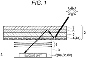
- Fig. 1 is a schematic cross-sectional view of an electronic apparatus 1 according to a first embodiment.
- the electronic apparatus 1 in Fig. 1 is an arbitrary electronic apparatus, such as a smartphone, a mobile phone, a tablet terminal, or a PC, having both a display function and an image capturing function.
- the electronic apparatus 1 in Fig. 1 includes a camera module (imaging unit) disposed on a side opposite to a display surface of a display unit 2.
- the electronic apparatus 1 in Fig. 1 is provided with a camera module 3 on a back side of the display surface of the display unit 2. Therefore, the camera module 3 captures an image through the display unit 2.
- Fig. 2(a) is a schematic external view of the electronic apparatus 1 in Fig. 1
- Fig. 2(b) is a cross-sectional view taken along a line A-A in Fig. 2(a)
- the display screen 1a spreads close to an outer size of the electronic apparatus 1, and a width of a bezel 1b around the display screen 1a is a few mm or less.
- a front camera is often mounted on the bezel 1b
- the camera module 3 that functions as a front camera is disposed on a back surface side of a substantially central portion of the display screen 1a.
- the camera module 3 is disposed on the back surface side of the substantially central portion of the display screen 1a in Fig. 2(a) , in the present embodiment, it is sufficient if the camera module 3 is disposed on the back surface side of the display screen 1a, and for example, the camera module 3 may be disposed near a peripheral edge on the back surface side of the display screen 1a.
- the camera module 3 in the present embodiment is disposed at an arbitrary position on the back surface side, the arbitrary portion overlapping the display screen 1a.
- the display unit 2 is a structure in which a display panel 4, a circularly polarizing plate 5, a touch panel 6, and a cover glass 7 are laminated in this order.
- the display panel 4 may be, for example, an organic light emitting device (OLED) unit, a liquid crystal display unit, a micro LED, or the display unit 2 based on another display principle.
- the display panel 4 such as the OLED unit includes a plurality of layers.
- the display panel 4 is often provided with a member having low transmittance such as a color filter layer.
- a through hole may be formed in a member having a low transmittance in the display panel 4 in accordance with a location where the camera module 3 is disposed. If the through hole is such that subject light passing through the through hole is incident on the camera module 3, image quality of an image captured by the camera module 3 can be improved.
- the circularly polarizing plate 5 is provided to reduce glare and enhance visibility of the display screen 1a even in a bright environment.
- a touch sensor is incorporated in the touch panel 6. There are various kinds of touch sensors such as a capacitive type or a resistive film type, and any type may be used. Furthermore, the touch panel 6 and the display panel 4 may be integrated.
- the cover glass 7 is provided to protect the display panel 4 and the like.
- the camera module 3 has an imaging unit 8 and an optical system 9.
- the optical system 9 is disposed on a light incident surface side of the imaging unit 8, that is, on a side close to the display unit 2, and condenses light on the imaging unit 8, the light passing through the display unit 2.
- the optical system 9 normally includes a plurality of lenses.
- the imaging unit 8 has a plurality of photoelectric conversion units 8a and a plurality of polarizing elements 8b.
- a photoelectric conversion unit 8a photoelectrically converts light incident via the display unit 2.
- the photoelectric conversion unit 8a may be a complementary metal oxide semiconductor (CMOS) sensor or a charge coupled device (CCD) sensor.
- CMOS complementary metal oxide semiconductor
- CCD charge coupled device
- the photoelectric conversion unit 8a may be a photodiode or an organic photoelectric conversion film.
- the plurality of photoelectric conversion units 8a can be arrayed in an arbitrary manner.
- An array system of the plurality of photoelectric conversion units 8a may be a Bayer array, an interline array, a checkered array, a stripe array, or another array.
- a plurality of polarizing elements 8b is disposed on a light incident side of at least one photoelectric conversion unit 8a among the plurality of photoelectric conversion units 8a.
- a polarizing element 8b polarizes incident light that passes through the display unit 2. The light polarized by the polarizing element 8b is incident on a corresponding photoelectric conversion unit 8a and is photoelectrically converted.
- polarization information an output value of a photoelectric conversion unit 8a that photoelectrically converts light polarized by a polarizing element 8b
- a pixel value or pixel information an output value of a photoelectric conversion unit 8a that photoelectrically converts light incident without passing through a polarizing element 8b.
- a combination of a polarizing element 8b and a photoelectric conversion unit 8a that photoelectrically converts light polarized by the polarizing element 8b is referred to as a polarization pixel
- a photoelectric conversion unit 8a that photoelectrically converts light incident without passing through the polarizing element 8b is referred to as a non-polarization pixel.
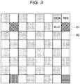
- Fig. 3 is a plan view illustrating an example of a pixel array of a plurality of polarization pixels 81 and a plurality of non-polarization pixels 82.
- the plurality of non-polarization pixels 82 for three RGB colors is disposed in two-dimensional directions, and the plurality of polarization pixels 81 is disposed separately from one another between the plurality of non-polarization pixels 82.
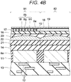
- Fig. 4A is a diagram illustrating a detailed cross-sectional structure of the imaging unit 8 according to the present embodiment.
- a plurality of photoelectric conversion units 8a is disposed in a substrate 11.
- a plurality of wiring layers 12 is disposed on a side close to a first surface 11a of the substrate 11.
- An interlayer insulation film 13 is disposed around the plurality of wiring layers 12.
- a light-shielding layer 15 is disposed in a vicinity of a boundary of a pixel, and a base insulation layer 16 is disposed around the light-shielding layer 15.
- a plurality of polarizing elements 8b is disposed separately from one another.
- Each of the polarizing elements 8b in Fig. 4A is a wire grid polarizing element that has a line-and-space structure and is disposed in a part of an insulation layer 17.
- Fig. 5 is a perspective view illustrating an example of a detailed structure of each of the polarizing elements 8b.
- each of the plurality of polarizing elements 8b has a plurality of line parts 8d having a protruding shape and extending in one direction, and a space part 8e between the respective line parts 8d.
- an angle formed by a direction in which a photoelectric conversion unit 8a is arrayed and a direction in which the line parts 8d extend may be four types of 0 degrees, 45 degrees, 90 degrees, and 135 degrees, or may be other angles.
- the plurality of polarizing elements 8b may polarize only in a single direction.
- a material of the plurality of polarizing elements 8b may be a metal material such as aluminum or tungsten, or an organic photoelectric conversion film.
- each of the polarizing elements 8b has a structure in which a plurality of line parts 8d extending in one direction is disposed separately from one another in a direction intersecting the one direction. There is a plurality of types of polarizing elements 8b with different extending directions of the line parts 8d. These polarizing elements 8b are disposed separately from one another so as to overlap with a part of a two-dimensional array of the plurality of photoelectric conversion units 8a.
- a line part 8d has a laminated structure in which a light reflection layer 8f, an insulation layer 8g, and a light absorption layer 8h are laminated.
- the light reflection layer 8f includes, for example, a metal material such as aluminum.
- the insulation layer 8g includes, for example, SiO2 or the like.
- the light absorption layer 8h is, for example, a metal material such as tungsten.
- a planarization layer 20 is disposed via protection layers 18 and 19.
- a color filter layer 21 is disposed on the planarization layer 20.
- the color filter layer 21 may have filter layers of the three RGB colors, or may have filter layers of cyan, magenta, and yellow that are complementary colors of the three RGB colors.
- a filter layer that transmits color other than visible light such as infrared light may be included, a filter layer having a multispectral characteristic may be included, or a filter layer of subtractive color, such as white, may be included.
- An on-chip lens 22 is disposed on the color filter layer 21.
- the on-chip lens 22 is disposed above the plurality of polarizing elements 8b in the cross-sectional structure in Fig. 4A
- the plurality of polarizing elements 8b may be disposed above the on-chip lens 22.
- the cross-sectional structure in Fig. 4B is similar to the cross-sectional structure in Fig. 4A except that the on-chip lens 22 and the plurality of polarizing elements 8b are laminated in a different order.
- a layer configuration of a part of the cross-sectional structures in Figs. 4A and 4B may be arbitrarily changed.
- the insulation layer 16 on which the plurality of polarizing elements 8b is disposed, and the color filter layer 21 may be integrated into one layer.
- Fig. 6A is a diagram schematically illustrating a state in which flare occurs when an image of a subject is captured by the electronic apparatus 1 in Fig. 1 .
- the flare occurs when a portion of light incident on the display unit 2 of the electronic apparatus 1 is repeatedly reflected by any of members in the display unit 2, and then is incident on the imaging unit 8 and captured in a taken image. If the flare occurs in the taken image, a luminance difference or a change in hue occurs as illustrated in Fig. 6A , and image quality is deteriorated.
- Fig. 6B is a diagram illustrating a signal component included in the taken image in Fig. 6A .
- a captured image includes a subject signal and a flare component.
- Figs. 7A, 7B , and 7C are diagrams conceptually describing correction processing according to the present embodiment.
- the imaging unit 8 according to the present embodiment has a plurality of polarization pixels 81 and a plurality of non-polarization pixels 82.
- Pixel information photoelectrically converted by the plurality of non-polarization pixels 82 illustrated in Fig. 7A includes a subject signal and a flare component as illustrated in Fig. 6B .
- polarization information photoelectrically converted by the plurality of polarization pixels 81 illustrated in Fig. 7A is flare component information.
- the flare component is removed and the subject signal is obtained. If an image based on the subject signal is displayed on the display unit 2, as illustrated in Fig. 7C , a subject image from which the flare existing in Fig. 6A has been removed is displayed.
- a subject image is affected by flare has been described in Figs. 6A to 6B and Figs. 7A to 7C
- the diffracted light may be incident on the imaging unit 8.
- the flare or the diffracted light may be captured in the taken image.
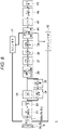
- Fig. 8 is a block diagram illustrating an internal configuration of the electronic apparatus 1 according to the present embodiment.
- the electronic apparatus 1 in Fig. 8 includes the optical system 9, the imaging unit 8, an A/D converter 31, a clamp unit 32, a color output unit 33, a polarization output unit 34, a flare extraction unit 35, a flare correction signal generation unit 36, a defect correction unit 37, a linear matrix unit 38, a gamma correction unit 39, a luminance chroma signal generation unit 40, a focus adjustment unit 41, an exposure adjustment unit 42, a noise reduction unit 43, an edge enhancement unit 44, and an output unit 45.
- the optical system 9 has one or more lenses 9a and an infrared ray (IR) cut filter 9b.
- the IR cut filter 9b may be omitted.
- the imaging unit 8 has the photoelectric conversion unit 8a having the plurality of non-polarization pixels 82 and the plurality of polarization pixels 81.
- Output values of the plurality of polarization pixels 81 and output values of the plurality of non-polarization pixels 82 are input to the A/D converter 31.
- the A/D converter 31 outputs polarization information data obtained by digitizing the output values of the plurality of polarization pixels 81 and digital pixel data obtained by digitizing the output values of the plurality of non-polarization pixels 82.
- the clamp unit 32 performs processing of defining a black level, and subtracts black level data from each of the digital pixel data and the polarization information data. Output data from the clamp unit 32 is branched, and thus RGB digital pixel data is output from the color output unit 33, and polarization information data is output from the polarization output unit 34.
- the flare extraction unit 35 extracts at least either a flare component or a diffracted light component from the polarization information data. In the present specification, at least either the flare component or diffracted light component extracted by the flare extraction unit 35 may be referred to as a correction amount.
- the flare correction signal generation unit 36 corrects the digital pixel data output from the color output unit 33 by performing, on the digital pixel data, processing of subtracting a correction amount extracted in the flare extraction unit 35.
- the output data from the flare correction signal generation unit 36 is digital pixel data from which at least either the flare component or the diffracted light component has been removed.
- the flare correction signal generation unit 36 functions as a correction unit that corrects, on the basis of the polarization information, the taken image photoelectrically converted by the plurality of non-polarization pixels 82.
- the digital pixel data at a pixel position of the polarization pixel 81 has a lower signal level by an amount passing through the polarizing element 8b. Therefore, the defect correction unit 37 regards the polarization pixel 81 as a defect and performs predetermined defect correction processing.
- the defect correction processing in this case may be processing of interpolation by using digital pixel data of surrounding pixel positions.
- the linear matrix unit 38 performs matrix operation on color information such as RGB to perform more correct color reproduction.
- the linear matrix unit 38 is also referred to as a color matrix unit.
- the gamma correction unit 39 performs gamma correction so as to enable display with excellent visibility in accordance with a display characteristic of the display unit 2. For example, the gamma correction unit 39 converts 10 bits into 8 bits while changing a gradient.
- the luminance chroma signal generation unit 40 generates, on the basis of the output data from the gamma correction unit 39, a luminance chroma signal to be displayed on the display unit 2.
- the focus adjustment unit 41 performs autofocus processing on the basis of a luminance chroma signal having been subjected to the defect correction processing.
- the exposure adjustment unit 42 performs exposure adjustment on the basis of the luminance chroma signal having been subjected to the defect correction processing.
- the exposure adjustment may be performed by providing an upper limit clip so that a pixel value of each of the non-polarization pixels 82 does not saturate.
- the pixel value of the saturated non-polarization pixel 82 may be estimated on the basis of a pixel value of a polarization pixel 81 around the non-polarization pixel 82.
- the noise reduction unit 43 performs processing of reducing noise included in the luminance chroma signal.
- the edge enhancement unit 44 performs processing of enhancing an edge in the subject image on the basis of the luminance chroma signal. Noise reduction processing by the noise reduction unit 43 and edge enhancement processing by the edge enhancement unit 44 may be performed only in a case where a predetermined condition is satisfied.
- the predetermined condition is, for example, a case where a correction amount of the flare component or diffracted light component extracted by the flare extraction unit 35 exceeds a predetermined threshold value.
- the more a flare component or diffracted light component included in a taken image the more noise or blurring of the edge occurs in an image from which the flare component or the diffracted light component is removed. Therefore, by performing the noise reduction processing or the edge enhancement processing only in a case where the correction amount exceeds the threshold value, frequency of performing the noise reduction processing or the edge enhancement processing can be reduced.
- Signal processing by at least some of the defect correction unit 37, the linear matrix unit 38, the gamma correction unit 39, the luminance chroma signal generation unit 40, the focus adjustment unit 41, the exposure adjustment unit 42, the noise reduction unit 43, and the edge enhancement unit 44 in Fig. 8 may be executed by a logic circuit in an image sensor having the imaging unit 8, or may be executed by a signal processing circuit in the electronic apparatus 1 equipped with the image sensor.
- signal processing of at least a part of Fig. 8 may be executed by a server or the like on a cloud, the server or the like transmitting and receiving information to and from the electronic apparatus 1 via a network. As illustrated in the block diagram in Fig.
- the flare correction signal generation unit 36 performs various kinds of signal processing on the digital pixel data from which at least either the flare component or the diffracted light component has been removed.
- this is because, in some signal processing such as exposure processing, focus adjustment processing, and white balance adjustment processing, a favorable signal processing result cannot be obtained even if the signal processing is performed in a state where a flare component or a diffracted light component is included.
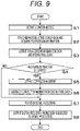
- Fig. 9 is a flowchart illustrating a processing procedure of image capturing processing performed by the electronic apparatus 1 according to the present embodiment.
- the camera module 3 is activated (step S1).
- power supply voltage is supplied to the imaging unit 8, and the imaging unit 8 starts imaging incident light.
- the plurality of non-polarization pixels 82 photoelectrically converts the incident light, and the plurality of polarization pixels 81 acquires polarization information of the incident light (step S2).
- the A/D converter 31 outputs polarization information data obtained by digitizing the output values of the plurality of polarization pixels 81 and digital pixel data obtained by digitizing the output values of the plurality of non-polarization pixels 82 (step S3).
- the flare extraction unit 35 determines whether or not flare or diffraction has occurred (step S4).
- the flare extraction unit 35 extracts a correction amount of the flare component or diffracted light component on the basis of the polarization information data (step S5).
- the flare correction signal generation unit 36 subtracts the correction amount from the digital pixel data to generate digital pixel data from which the flare component or the diffracted light component has been removed (step S6).
- step S7 various kinds of signal processing are performed on the digital pixel data corrected in step S6 or the digital pixel data for which, in step S4, it is determined that flare or diffraction has not occurred (step S7). More specifically, in step S7, as illustrated in Fig. 8 , processing such as defect correction processing, linear matrix processing, gamma correction processing, luminance chroma signal generation processing, exposure processing, focus adjustment processing, white balance adjustment processing, noise reduction processing, or edge enhancement processing is performed. Note that a type and execution order of the signal processing are arbitrary, and signal processing of some blocks illustrated in Fig. 8 may be omitted, or signal processing other than the blocks illustrated in Fig. 8 may be performed.
- the digital pixel data having been subjected to the signal processing in step S7 may be output from the output unit 45 and stored in an unillustrated memory, or may be displayed on the display unit 2 as a live image (step S8).
- the camera module 3 is disposed on the side opposite to the display surface of the display unit 2, and polarization information of light passing through the display unit 2 is acquired by the plurality of polarization pixels 81. A portion of the light passing through the display unit 2 is repeatedly reflected in the display unit 2, and then is incident on the plurality of non-polarization pixels 82 in the camera module 3.
- polarization information by acquiring the above-described polarization information, it is possible to generate a taken image in a state where a flare component or diffracted light component included in light incident on the plurality of non-polarization pixels 82 after being repeatedly reflected in the display unit 2 is simply and reliably removed.
- digital pixel data from which a flare component or a diffracted light component has been removed can be generated by performing, on digital pixel data imaged and A/D-converted by the plurality of non-polarization pixels 82 that photoelectrically converts light incident without passing through a polarizing element 8b, processing of subtracting a correction amount based on polarization information acquired by the plurality of polarization pixels 81.
- a degree of noise removal in the noise reduction processing may be adjusted according to a magnitude of the correction amount by the flare component or the diffracted light component. More specifically, the larger the correction amount, the higher the degree of noise removal in the noise reduction processing. Furthermore, in a case where an edge becomes unclear by further increasing the degree of noise removal in the noise reduction processing, a degree of edge enhancement in the edge enhancement processing may be further increased.
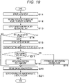
- Fig. 10 is a flowchart illustrating a processing procedure of image capturing processing performed by an electronic apparatus 1 according to the present embodiment. Because the processing from steps S11 to S16 is similar to steps S1 to S6 in Fig. 9 , the description thereof will be omitted.
- step S17 it is determined whether or not the correction amount extracted in step S14 exceeds a predetermined threshold value (step S17). If it is determined that the correction amount exceeds the threshold value, at least either the degree of noise removal in the noise reduction processing or the degree of edge enhancement in the edge enhancement processing is further increased (step S18).
- step S19 normal noise reduction processing and edge enhancement processing are performed.
- step S20 In a case where it is determined in step S14 that no flare or diffraction has occurred, or in a case where the processing in step S18 has ended, or in a case where the processing in step S19 has ended, other signal processing is performed (step S20). When all the signal processing is completed, digital pixel data is output (step S21).
- Fig. 10 illustrates an example in which a degree of noise reduction processing or edge enhancement processing is increased in a case where a correction amount exceeds a threshold value
- a parameter adjustment unit that adjusts a parameter for when performing arbitrary signal processing according to the correction amount. Because it is conceivable that an amount of adjusting the parameter varies depending on content of the signal processing, the parameter adjustment unit may set, according to the correction amount, an optimum parameter for each unit that performs each signal processing.
- the noise reduction unit 43 and the edge enhancement unit 44 also serve as the parameter adjustment unit.
- the noise reduction unit 43 adjusts a parameter for deciding a degree of noise removal
- the edge enhancement unit 44 adjusts a parameter for deciding a degree of edge enhancement.
- a degree of the noise reduction processing or edge enhancement processing is switched in two ways depending on whether or not the correction amount exceeds the threshold value
- the degree of the noise reduction processing or edge enhancement processing may be switched in finer three or more stages according to the correction amount of the flare component or diffracted light component, a state of the subject, or the like.
- an S/N ratio of the digital pixel data having been subjected to the subtraction may decrease by subtracting the correction amount based on the flare component or the diffracted light component from the digital pixel data
- processing of further increasing the degree of noise removal or the degree of edge enhancement is performed.
- each pixel has a divided structure.
- Fig. 11 is a plan view illustrating an example of a pixel array of a plurality of polarization pixels 81 and a plurality of non-polarization pixels 82 according to the third embodiment.
- each of the polarization pixels 81 and each of the non-polarization pixels 82 are divided into four.
- each of photoelectric conversion units 8a includes a plurality of divided photoelectric conversion units, and light polarized by a plurality of polarizing elements 8b is incident on the plurality of divided photoelectric conversion units in some of the photoelectric conversion units 8a. Note that, although Fig.
- each of the polarization pixels 81 and each of the non-polarization pixels 82 are divided into four, each of the polarization pixels 81 and each of the non-polarization pixels 82 may be divided into any number equal to or greater than two.
- the plurality of polarization pixels 81 is provided corresponding to positions and sizes of the plurality of non-polarization pixels 82, and in the example in Fig. 11 , one polarization pixel 81 is provided for five non-polarization pixels 82 in each of a horizontal direction and a vertical direction.
- Each of the polarization pixels 81 is divided into four similarly to each of the non-polarization pixels 82.
- Polarization patterns of four divided pixels in the same polarization pixel 81 are the same.
- the example in Fig. 11 is a case where four types of polarization pixels 81 having different polarization patterns are included, the number of types of the polarization pixels 81 is arbitrary as long as the number of types is three or more.
- each pixel obtained by dividing each of the polarization pixels 81 or each of the non-polarization pixels 82 into four is referred to as a divided pixel.
- an on-chip lens 22 may be separately provided for each of the four divided pixels that constitute each of the non-polarization pixels 82.
- a size of each of the polarization pixels 81 is the same as a size of each of the non-polarization pixels 82, and each of the polarization pixels 81 is disposed according to a location where each of the non-polarization pixels 82 is disposed, the size of each of the polarization pixels 81 or a location where each of the polarization pixels 81 is disposed may be different from the size of each of the non-polarization pixels 82 or a location where each of the non-polarization pixels 82 is disposed.
- Fig. 12 is a plan view illustrating a first modification of the divided structure.
- three of four divided pixels that constitute one pixel are utilized for photoelectric conversion of a corresponding non-polarization pixel 82, and a remaining one divided pixel is utilized as a polarization pixel 81.
- a photoelectric conversion unit 8a includes a plurality of divided photoelectric conversion units, and light polarized by a plurality of polarizing elements 8b is incident on some of the divided photoelectric conversion units in any of the photoelectric conversion units 8a.
- a polarization pixel 81 and a non-polarization pixel 82 are partially disposed inside each pixel.
- an on-chip lens is provided corresponding to each of the four divided pixels that constitute one pixel.
- One polarization pixel 81 is provided for a plurality of non-polarization pixels 82 in the example in Fig. 11 , whereas a non-polarization pixel 82 and a polarization pixel 81 are provided for each pixel in the example in Fig. 12 . Therefore, in the example in Fig. 12 , polarization information in a photoelectric conversion unit 8a can be acquired more accurately than in the example in Fig. 11 .
- the number of types of the polarization patterns is only required to be three or more, and is not limited to four.
- a pixel output value is decided on the basis of output values of divided photoelectric conversion units for three divided pixels that are among two divided pixels each in the vertical and horizontal directions and are utilized as non-polarization pixels 82, and a correction amount is decided on the basis of an output value of a divided photoelectric conversion unit for one divided pixel that is among the two divided pixels each in the vertical and horizontal directions and is utilized as a polarization pixel 81.
- each pixel partially includes non-polarization pixels 82, and therefore it is not necessary to perform defect correction, and signal processing can be simplified.
- a correction amount based on a flare component or diffracted light component can be calculated by a polarization pixel 81 allocated to a part of each pixel, and the flare component or the diffracted light component can be removed from a taken image by subtracting the correction amount from digital pixel data.
- a polarization pixel 81 is allocated to one of four divided pixels obtained by dividing each pixel, and therefore a size of the polarization pixel 81 is very small.
- the polarization pixel 81 includes, for example, line and space parts as illustrated in Fig. 5 , it is not easy to accurately make shapes of line parts 8d uniform or accurately align intervals between two adjacent line parts 8d by using microfabrication technology. Therefore, a size of the polarization pixel 81 may be larger than a size of the non-polarization pixels 82.
- Fig. 13 is a plan view illustrating a second modification of the divided structure.
- one polarization pixel 81 is disposed so as to extend over four pixels disposed adjacent to one another.
- a photoelectric conversion unit 8a includes a plurality of divided photoelectric conversion units, and light polarized by a polarizing element 8b is incident on a divided conversion unit for each unit of two or more photoelectric conversion units 8a.
- a size of the polarization pixel 81 is twice a size of a pixel in the vertical and horizontal directions, and an area of the polarization pixel 81 is four times an area of the pixel.
- Fig. 13 is a plan view illustrating a second modification of the divided structure.
- one polarization pixel 81 is disposed so as to extend over four pixels disposed adjacent to one another.
- a photoelectric conversion unit 8a includes a plurality of divided photoelectric conversion units, and light polarized by a polarizing element 8b is incident on a divided conversion unit for each unit of
- each pixel has divided pixels utilized as non-polarization pixels 82, and therefore it is not necessary to perform defect correction
- an on-chip lens 22 is provided separately. Remaining one divided pixel is, along with other three divided pixels adjacent thereto, provided with one large on-chip lens 22, and is utilized as a polarization pixel 81.
- a large polarizing element 8b by producing a large polarizing element 8b by utilizing a region of four divided pixels disposed adjacent to one another and providing an on-chip lens 22 corresponding to a size of the polarizing element 8b, the polarizing element 8b can be easily manufactured, and highly reliable polarization information can be acquired.
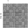
- Fig. 14 is a plan view illustrating a third modification of the divided structure.
- a polarization pixel 81 is disposed on an entire pixel region. More specifically, a plurality of photoelectric conversion units 8a has a plurality of divided photoelectric conversion units, and light polarized by a plurality of polarizing elements 8b is incident on the plurality of photoelectric conversion units 8a. That is, in the example in Fig. 14 , only polarization pixels 81 exist, and non-polarization pixels 82 do not exist. In the example in Fig. 14 , each pixel is divided into four divided pixels, and all of the divided pixels are used as polarization pixels 81.
- a polarization pixel 81 is allocated to all of the divided pixels in all the pixels, and therefore output values of the photoelectric conversion units 8a decrease uniformly. Therefore, gain adjustment processing for entirely increasing the output values of the photoelectric conversion units 8a may be performed. Although an S/N ratio may decrease by performing the gain adjustment processing, it is possible to generate highly reliable digital pixel data by performing processing of further increasing a degree of the noise reduction processing or of the edge enhancement processing, or the like.
- a polarizing element 8b in association with an entire region of a photoelectric conversion unit 8a as illustrated in Fig. 14 , it is possible to acquire polarization information in consideration of an effect of flare or diffracted light incident on an arbitrary location in the photoelectric conversion unit 8a. Therefore, accuracy of the correction amount extracted by a flare extraction unit 35 can be improved.
- Fig. 15 is a plan view illustrating a fourth modification of the divided structure.
- the example in Fig. 15 is common to Fig. 3 and the like in that a polarization pixel 81 is disposed between non-polarization pixels 82, and is different from the above-described other divided structures in that each of the non-polarization pixels 82 is divided into two right and left divided pixels.
- a photoelectric conversion unit 8a has a plurality of divided photoelectric conversion units divided into two or more in one direction and capable of detecting phase difference information, and light polarized by a polarizing element 8b is incident on a plurality of divided photoelectric conversion units in any of the photoelectric conversion units 8a.
- Each of the divided pixels has, for example, a vertically long rectangular shape.
- the two divided pixels can be used for detecting phase difference information. For example, focusing can be performed on the basis of the phase difference information.
- Each of the polarization pixels 81 provided at a ratio of 1 to a plurality of non-polarization pixels 82 (five non-polarization pixels 82, for example) in Fig. 15 has two divided pixel sizes. As described above, because a polarizing element 8b has line and space parts, microfabrication thereof is not easy. However, a polarizing element 8b in Fig. 15 has twice a size of a divided pixel, and therefore manufacturing thereof is relatively easy, and a manufacturing defect is less likely to occur.
- Figs. 11 to 15 described above illustrate representative examples of the divided structure, and there may be a divided structure other than the illustrated divided structures.
- the present embodiment can be applied to all divided structures, and a photoelectric conversion unit 8a may be divided into any shapes and sizes. Therefore, a division shape and division size of the non-polarization pixels 82, and the division number of the non-polarization pixels 82 are arbitrary. Furthermore, the polarization pixels 81 may be divided or may not be divided.
- the non-polarization pixels 82 have a divided structure, if a part of the divided pixels in each pixel is allocated to a polarization pixel 81 to acquire polarization information, and remaining divided pixels are allocated to non-polarization pixels 82 to acquire color information, it is not necessary to perform defect correction on each pixel.
- phase difference information can be detected by each pixel having a divided structure.
- a size of the polarization pixel 81 can be larger than a size of the non-polarization pixels 82, and therefore the polarizing elements 8b can be easily manufactured.
- a structure of a display unit 2 is characterized in an electronic apparatus 1 in which a camera module 3 is disposed on a side opposite to a display surface of the display unit 2.
- a circularly polarizing plate 5 is provided inside the display unit 2 in order to improve visibility.
- the circularly polarizing plate 5 shields at least a portion of light, if subject light that has passed through the display unit 2 is imaged by the camera module 3, a problem such as a dark taken image occurs.
- transmittance of a touch sensor inside the display unit 2, a display panel 4 such as an OLED unit, and the like is not very high. Therefore, in the present embodiment, a through hole is provided in a region overlapping the camera module 3 in the display unit 2 in a front-back direction.
- Fig. 16 is a schematic cross-sectional view of the electronic apparatus 1 according to the fourth embodiment.
- the display unit 2 in the electronic apparatus 1 in Fig. 16 has a plurality of through holes 2a in portions overlapping the camera module 3 in the front-back direction. These through holes 2a are provided in a plurality of layers having low transmittance such as the touch sensor, circularly polarizing plate 5, and display panel 4 in the display unit 2.
- a size of a diameter of a through hole 2a varies with each layer.
- the circularly polarizing plate 5 has a through hole 2a having a diameter of the same size as a diameter of an imaging unit 8 of the camera module 3.
- the touch sensor and the display panel 4 may be provided with a plurality of small through holes 2a within the diameter size of the imaging unit 8 so as not to adversely affect display or touch sensitivity of the display unit 2 as much as possible.
- through holes 2a may slightly affect visibility or touch sensitivity of a display screen 1a of the display unit 2, there is almost no problem in practical use, because a size of a diameter of the camera module 3 is about merely a few mm.
- transmittance of subject light passing through the display unit 2 is improved, and image quality of an image taken by the camera module 3 can be improved.
- Fig. 17 is a cross-sectional view of a first modification in which a structure of the display unit 2 is characterized.
- a polarization member 2b that polarizes light in a specific direction is disposed on a back surface of the display panel 4.
- the polarization member 2b is disposed on a back surface side of a region not vertically overlapping the camera module 3 in the display panel 4.
- the polarization member 2b When light incident on the display unit 2 is incident on the polarization member 2b, the light is polarized in a specific direction when reflected. The reflected light is further reflected by another layer of the display unit 2, for example, and is incident on the imaging unit 8. Because the reflected light is polarized in a specific direction when being incident on the imaging unit 8, polarization information of the light polarized by the polarization member 2b can be reliably acquired by previously providing at least some of a plurality of polarizing elements 8b with the same polarization characteristic as a polarization characteristic of the polarization member 2b.
- polarization member 2b polarized in a specific direction in the display unit 2
- light incident on the imaging unit 8 can be polarized in a specific direction, and a flare component or a diffraction component can be more reliably extracted by a plurality of polarization pixels 81.
- Fig. 18 is a cross-sectional view of a second modification in which a structure of the display unit 2 is characterized.
- the polarization member 2b polarized in a specific direction is provided in a region in the circularly polarizing plate 5, the region overlapping the camera module 3 in the front-back direction.
- the camera module 3 intends to image light incident substantially parallel to an optical axis. Therefore, the polarization member 2b that polarizes light in a direction substantially parallel to the optical axis is provided beforehand in, for example, a region overlapping the camera module 3 of the circularly polarizing plate 5 in the front-back direction.
- transmittance when light passes through the display unit 2 can be improved, and image quality of an image taken by the camera module 3 can be improved.
- transmittance when light passes through the display unit 2 can be improved, and image quality of an image taken by the camera module 3 can be improved.
- the polarization member 2b polarized in a specific direction in at least a part of the display unit 2 by providing the polarization member 2b polarized in a specific direction in at least a part of the display unit 2, light that is repeatedly reflected in the display unit 2 and then is incident on the imaging unit 8 can be polarized in a specific direction, and the light can be reliably received by the polarization pixel 81.
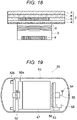
- Fig. 19 is a plan view in a case where the electronic apparatus 1 according to the first to fourth embodiments is applied to a capsule endoscope 50.
- the capsule endoscope 50 in Fig. 19 includes, in a housing 51 with both end surfaces having a hemispherical shape and a central portion having a cylindrical shape for example, a camera (ultracompact camera) 52 for capturing an image of inside a body cavity, a memory 53 for recording image data captured by the camera 52, and a wireless transmitter 55 for transmitting the recorded image data to an outside via an antenna 54 after the capsule endoscope 50 is discharged to outside of a test subject.
- a camera ultracompact camera
- a central processing unit (CPU) 56 and a coil (magnetic force/current conversion coil) 57 are provided in the housing 51.
- the CPU 56 controls image capturing by the camera 52 and operation of accumulating data in the memory 53, and controls data transmission from the memory 53 to a data reception device (not illustrated) outside the housing 51 by the wireless transmitter 55.
- the coil 57 supplies power to the camera 52, the memory 53, the wireless transmitter 55, the antenna 54, and a light source 52b as described later.
- the housing 51 is provided with a magnetic (reed) switch 58 for sensing that the capsule endoscope 50 is set on the data reception device.
- the CPU 56 supplies power from the coil 57 to the wireless transmitter 55 at a time point when the reed switch 58 senses the set on the data reception device and data transmission becomes possible.
- the camera 52 has, for example, an imaging element 52a including an objective optical system 9 for capturing an image in a body cavity, and a plurality of light sources 52b for illuminating the body cavity.
- the camera 52 includes a complementary metal oxide semiconductor (CMOS) sensor, a charge coupled device (CCD), or the like including a light emitting diode (LED) for example, as a light source 52b.
- CMOS complementary metal oxide semiconductor
- CCD charge coupled device
- LED light emitting diode
- a display unit 2 in the electronic apparatus 1 is a concept including a luminous object such as a light source 52b in Fig. 19 .
- the capsule endoscope 50 in Fig. 19 includes, for example, two light sources 52b, and these light sources 52b can be configured by a display panel 4 having a plurality of light source units or an LED module having a plurality of LEDs. In this case, by disposing an imaging unit 8 of the camera 52 below the display panel 4 or the LED module, a restriction on layout arrangement of the camera 52 is reduced, and a smaller capsule endoscope 50 can be implemented.
- Fig. 20 is a rear view in a case where an electronic apparatus 1 according to the first to fourth embodiments is applied to a digital single-lens reflex camera 60.
- the digital single-lens reflex camera 60 or a compact camera includes a display unit 2 that displays a preview screen on a rear surface on a side opposite to a lens.
- a camera module 3 may be disposed on a side opposite to a display surface of the display unit 2 so that a face image of a person who captures the face image can be displayed on a display screen 1a of the display unit 2.
- the camera module 3 can be disposed in a region overlapping the display unit 2, and therefore it is not necessary to provide the camera module 3 on a frame part of the display unit 2, and a size of the display unit 2 can be increased as much as possible.
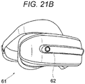
- Fig. 21A is a plan view illustrating an example in which the electronic apparatus 1 according to the first to fourth embodiments is applied to a head mounted display (hereinafter, HMD) 61.
- the HMD 61 in Fig. 21A is utilized for virtual reality (VR), augmented reality (AR), mixed reality (MR), substitutional reality (SR), or the like.
- a current HMD is equipped with a camera 62 on an outer surface thereof, and there is a problem that, although a wearer of the HMD can visually recognize a surrounding image, a human around the wearer of the HMD cannot recognize expression of eyes or face of the wearer of the HMD.
- the display surface of the display unit 2 is provided on an outer surface of the HMD 61, and the camera module 3 is provided on a side opposite to the display surface of the display unit 2.
- the camera module 3 is provided on a side opposite to the display surface of the display unit 2.
- the camera module 3 is provided on a back surface side of the display unit 2, and therefore there is no restriction on an installation location of the camera module 3, and design of the HMD 61 can be highly flexible. Furthermore, because the camera can be disposed at an optimum position, it is possible to prevent a problem such as deviation of a line of sight of the wearer displayed on the display surface.
- the electronic apparatus 1 according to the first to fourth embodiments can be used for various kinds of applications, and a utility value can be enhanced.
- the type of the light source may be estimated in calculating a correction amount of a flare component or a diffracted light component.
- Fig. 22 is a block diagram illustrating a schematic configuration of the electronic apparatus 1 according to a sixth embodiment.
- the electronic apparatus 1 in Fig. 22 includes a light source estimation unit 46 in addition to the configuration in Fig. 8 .
- the light source estimation unit 46 estimates a light source of light incident on the display unit 2.
- the light source estimation unit 46 may estimate the light source on the basis of a difference in sensitivity of each RGB color photoelectrically converted by a photoelectric conversion unit 8a, or may estimate the light source by using an illuminance sensor, a multispectral sensor, or the like.
- a GPS sensor mounted on the electronic apparatus 1 may discriminate whether the electronic apparatus 1 is indoors or outdoors to estimate whether the light source is sunlight or illumination light.
- a tilt angle of the electronic apparatus 1 may be determined by a gyro sensor mounted on the electronic apparatus 1, and the light source may be estimated on the basis of the tilt angle.
- a flare correction signal generation unit 36 adjusts a correction amount of a taken image photoelectrically converted by a plurality of non-polarization pixels 82 on the basis of the light source estimated by the light source estimation unit 46. More specifically, a mathematical formula for calculating the correction amount may be changed for each type of light source. Furthermore, the correction amount may be individually adjusted for each RGB color for each type of light source.
- Fig. 23 is a block diagram illustrating a schematic configuration of the electronic apparatus 1 according to a modification of the sixth embodiment.
- the electronic apparatus 1 in Fig. 23 includes a luminance estimation unit 47 in addition to the configuration in Fig. 8 .
- the luminance estimation unit 47 estimates the display luminance of the display unit 2.
- the luminance estimation unit 47 estimates the display luminance of the display unit 2 on the basis of, for example, a signal from an unillustrated display control unit that performs display control of the display unit 2.
- the flare correction signal generation unit 36 adjusts a correction amount of a taken image photoelectrically converted by the plurality of non-polarization pixels 82 on the basis of the display luminance of the display unit 2 estimated by the luminance estimation unit 47. More specifically, the correction amount may be individually adjusted for each color on the basis of luminance of each RGB color displayed on the display unit 2.
- the electronic apparatus 1 including both the light source estimation unit 46 in Fig. 22 and the luminance estimation unit 47 in Fig. 23 is also conceivable.
- the flare correction signal generation unit 36 adjusts the correction amount on the basis of the type of the light source and the display luminance of the display unit 2.
- a correction amount for correcting an effect of a flare component or a diffracted light component is adjusted in consideration of a type of a light source incident on the electronic apparatus 1 or display luminance of the display unit 2, and therefore the flare component and the diffracted light component can be more appropriately removed from a taken image.
- an optical system 9 of a camera module 3 is different from an optical system 9 of the first to sixth embodiments.
- Fig. 24 is a diagram illustrating a cross-sectional structure of an imaging unit 8 of the camera module 3 mounted on the electronic apparatus 1 according to the seventh embodiment.
- the imaging unit 8 in Fig. 24 has a microlens array 64, instead of a single lens or a lens group in which single lenses are arranged in an optical axis direction.
- the imaging unit 8 in Fig. 24 has a photoelectric conversion unit 8a disposed along a bottom surface of a housing 63, the microlens array 64 disposed above the photoelectric conversion unit 8a, a plurality of light shielding bodies 66 disposed between microlenses 65 adjacent to one another, and a light guide plate 67 disposed above the microlens array 64.
- microlens array 64 as the optical system 9 of the imaging unit 8, it is possible to prevent an effect of an adjacent pixel and to reduce color blurring.
- an electronic apparatus 1 is applicable not only to removal of flare or diffracted light but also, for example, to a purpose of removing shininess of a subject.
- a camera module 3 can be disposed on a side opposite to a display surface of a display unit 2, and therefore, in a case where a wide-angle or fisheye lens is attached to the camera module 3, an entire display surface of the display unit 2 can be imaged by the camera module 3.
- a plurality of polarization pixels 81 having a plurality of polarizing elements 8b may acquire polarization information caused by a shininess component included in subject light.
- a flare extraction unit 35 in Fig. 8 extracts a correction amount based on the shininess component.
- a flare correction signal generation unit 36 generates an image obtained by removing the shininess component from a subject image.
- a camera module 3 is disposed on a side opposite to a display surface of a display unit 2 in each of the above-described embodiments, in a case where there is a reflector plate in a lowermost layer of a display panel 4 such as an OLED unit, a portion of the reflector plate may be hollowed out to dispose the camera module 3 on the hollowed portion, or the camera module 3 may be disposed so as to bite into a portion of the display panel 4.
Landscapes
- Engineering & Computer Science (AREA)
- Signal Processing (AREA)
- Multimedia (AREA)
- Physics & Mathematics (AREA)
- General Physics & Mathematics (AREA)
- Optics & Photonics (AREA)
- Spectroscopy & Molecular Physics (AREA)
- Studio Devices (AREA)
- Solid State Image Pick-Up Elements (AREA)
- Devices For Indicating Variable Information By Combining Individual Elements (AREA)
- Transforming Light Signals Into Electric Signals (AREA)
Applications Claiming Priority (2)
| Application Number | Priority Date | Filing Date | Title |
|---|---|---|---|
| JP2019184761 | 2019-10-07 | ||
| PCT/JP2020/038005 WO2021070867A1 (ja) | 2019-10-07 | 2020-10-07 | 電子機器 |
Publications (2)
| Publication Number | Publication Date |
|---|---|
| EP4044574A1 true EP4044574A1 (de) | 2022-08-17 |
| EP4044574A4 EP4044574A4 (de) | 2022-11-09 |
Family
ID=74942758
Family Applications (1)
| Application Number | Title | Priority Date | Filing Date |
|---|---|---|---|
| EP20874260.1A Withdrawn EP4044574A4 (de) | 2019-10-07 | 2020-10-07 | Elektronische vorrichtung |
Country Status (7)
| Country | Link |
|---|---|
| US (1) | US11917306B2 (de) |
| EP (1) | EP4044574A4 (de) |
| JP (1) | JP7667085B2 (de) |
| KR (1) | KR20220072834A (de) |
| CN (2) | CN212727101U (de) |
| TW (1) | TWI853102B (de) |
| WO (1) | WO2021070867A1 (de) |
Cited By (1)
| Publication number | Priority date | Publication date | Assignee | Title |
|---|---|---|---|---|
| EP4102816A4 (de) * | 2020-02-03 | 2023-08-16 | Sony Semiconductor Solutions Corporation | Elektronische vorrichtung |
Families Citing this family (4)
| Publication number | Priority date | Publication date | Assignee | Title |
|---|---|---|---|---|
| TWI853102B (zh) * | 2019-10-07 | 2024-08-21 | 日商索尼半導體解決方案公司 | 電子機器 |
| WO2021092887A1 (en) * | 2019-11-15 | 2021-05-20 | Qualcomm Incorporated | Display shade compensation for cameras |
| JP2024092602A (ja) * | 2022-12-26 | 2024-07-08 | ソニーセミコンダクタソリューションズ株式会社 | 光検出素子及び電子機器 |
| US20250220315A1 (en) * | 2023-12-27 | 2025-07-03 | Varjo Technologies Oy | High-dynamic range imaging using partial polarisation mask |
Family Cites Families (54)
| Publication number | Priority date | Publication date | Assignee | Title |
|---|---|---|---|---|
| US8022977B2 (en) * | 2005-10-17 | 2011-09-20 | I2Ic Corporation | Camera placed behind a display with a transparent backlight |
| JP4728793B2 (ja) * | 2005-12-14 | 2011-07-20 | 株式会社アイ・オー・データ機器 | ディスプレイ装置およびその制御方法 |
| JP5176397B2 (ja) * | 2006-06-01 | 2013-04-03 | ソニー株式会社 | 表示装置及びその駆動方法 |
| CN102017601B (zh) * | 2008-06-26 | 2013-03-13 | 松下电器产业株式会社 | 图像处理装置及图像合成方法 |
| JP5607911B2 (ja) * | 2009-10-21 | 2014-10-15 | オリンパスイメージング株式会社 | 画像処理装置、撮像装置、画像処理方法、および、画像処理プログラム |
| JP5459085B2 (ja) * | 2010-06-07 | 2014-04-02 | ソニー株式会社 | 画像表示装置、電子機器、画像表示システム、画像取得方法、プログラム |
| US9013613B2 (en) * | 2010-09-21 | 2015-04-21 | Sony Corporation | Sensor-equipped display apparatus and electronic apparatus |
| JP6041495B2 (ja) * | 2011-03-24 | 2016-12-07 | キヤノン株式会社 | 撮像装置及び欠陥画素の判定方法 |
| JP5831024B2 (ja) * | 2011-08-04 | 2015-12-09 | ソニー株式会社 | 画像処理装置、および画像処理方法、並びにプログラム |
| US8947627B2 (en) | 2011-10-14 | 2015-02-03 | Apple Inc. | Electronic devices having displays with openings |
| WO2013175686A1 (ja) * | 2012-05-22 | 2013-11-28 | パナソニック株式会社 | 撮像処理装置および内視鏡 |
| JP2014011754A (ja) * | 2012-07-03 | 2014-01-20 | Sony Corp | 制御装置、制御方法、及びプログラム |
| EP2957215B1 (de) * | 2013-02-15 | 2020-05-06 | Panasonic Intellectual Property Management Co., Ltd. | Bildverarbeitungsvorrichtung und endoskop |
| JP2015026937A (ja) * | 2013-07-25 | 2015-02-05 | ソニー株式会社 | 撮像装置および撮像方法、並びにプログラム |
| JP6379966B2 (ja) * | 2013-12-24 | 2018-08-29 | 株式会社リコー | 画像処理装置、画像処理システム、画像処理方法、画像処理プログラム、及び移動体制御装置 |
| JP6288569B2 (ja) * | 2014-02-28 | 2018-03-07 | パナソニックIpマネジメント株式会社 | 固体撮像素子及びその製造方法 |
| US9945718B2 (en) * | 2015-01-07 | 2018-04-17 | Semiconductor Components Industries, Llc | Image sensors with multi-functional pixel clusters |
| JP2016146583A (ja) * | 2015-02-09 | 2016-08-12 | 株式会社リコー | 撮像装置、移動体機器制御システム及びプログラム |
| EP3264754B1 (de) * | 2015-02-27 | 2022-02-16 | Sony Group Corporation | Bildverarbeitungsvorrichtung, bildverarbeitungsverfahren und bilderfassungselement |
| JP2016171368A (ja) * | 2015-03-11 | 2016-09-23 | 株式会社東芝 | 撮像装置、撮像素子、及び撮像方法 |
| JP6247794B2 (ja) * | 2015-04-23 | 2017-12-13 | 富士フイルム株式会社 | 画像処理装置、撮像装置、画像処理方法、及びプログラム |
| JP2017005111A (ja) * | 2015-06-10 | 2017-01-05 | ソニー株式会社 | 固体撮像装置及び電子機器 |
| JP6566749B2 (ja) * | 2015-07-01 | 2019-08-28 | 株式会社ソニー・インタラクティブエンタテインメント | 撮像素子、イメージセンサ、および情報処理装置 |
| US10298863B2 (en) * | 2015-09-08 | 2019-05-21 | Apple Inc. | Automatic compensation of lens flare |
| CN108293093B (zh) * | 2015-11-19 | 2020-11-03 | 索尼公司 | 图像处理设备和图像处理方法 |
| KR20170111827A (ko) * | 2016-03-29 | 2017-10-12 | 삼성전자주식회사 | 디스플레이 및 카메라를 포함하는 전자 장치 |
| JP6697680B2 (ja) * | 2016-08-17 | 2020-05-27 | ソニー株式会社 | 信号処理装置、信号処理方法、およびプログラム |
| DE112017004203T5 (de) * | 2016-08-24 | 2019-06-13 | Sony Corporation | Bildverarbeitungsvorrichtung, informationserzeugungsvorrichtung und informationserzeugungsverfahren |
| JP2018037722A (ja) * | 2016-08-29 | 2018-03-08 | ソニーセミコンダクタソリューションズ株式会社 | 撮像装置 |
| US10897148B2 (en) | 2016-09-23 | 2021-01-19 | Apple Inc. | Wireless charging mats with multi-layer transmitter coil arrangements |
| JP7070423B2 (ja) * | 2016-10-17 | 2022-05-18 | ソニーグループ株式会社 | 画像処理装置と画像処理方法および撮像装置 |
| EP3544283B1 (de) * | 2016-11-15 | 2023-07-19 | Sony Group Corporation | Bildverarbeitungsvorrichtung |
| US11424284B2 (en) * | 2017-03-03 | 2022-08-23 | Sony Semiconductor Solutions Corporation | Solid-state imaging device and electronic apparatus |
| WO2018173754A1 (ja) * | 2017-03-24 | 2018-09-27 | ソニーセミコンダクタソリューションズ株式会社 | 積層型撮像素子及び固体撮像装置 |
| US10652497B2 (en) * | 2017-04-21 | 2020-05-12 | Trustees Of Dartmouth College | Quanta image sensor with polarization-sensitive jots |
| US11108951B2 (en) * | 2017-06-13 | 2021-08-31 | Sony Corporation | Image capturing device and imaging element, and image processing method |
| JP7105062B2 (ja) * | 2017-12-21 | 2022-07-22 | 株式会社ソニー・インタラクティブエンタテインメント | 画像処理装置、コンテンツ処理装置、コンテンツ処理システム、および画像処理方法 |
| CN112106343A (zh) * | 2018-03-29 | 2020-12-18 | 索尼公司 | 信息处理装置、信息处理方法、程序和信息处理系统 |
| CN108810201B (zh) * | 2018-06-04 | 2020-07-17 | Oppo广东移动通信有限公司 | 电子装置及利用电子装置拍摄照片的方法 |
| EP3805717B1 (de) * | 2018-06-05 | 2023-05-17 | Sony Group Corporation | Vorrichtung zur informationserzeugung, verfahren zur informationserzeugung und programm |
| CN109948410B (zh) * | 2018-07-20 | 2020-09-11 | 华为技术有限公司 | 具有纹路检测功能的电子设备 |
| US11252362B2 (en) * | 2018-08-31 | 2022-02-15 | Sony Semiconductor Solutions Corporation | Imaging element, imaging device, and imaging method |
| KR102534247B1 (ko) * | 2018-10-01 | 2023-05-18 | 삼성전자주식회사 | 편광판을 포함한 3d 이미지 센서, 및 그 3d 이미지 센서를 기반으로 한 깊이 보정방법과 3d 영상 생성방법 |
| JPWO2020085149A1 (ja) * | 2018-10-22 | 2021-09-16 | 富士フイルム株式会社 | 撮像装置及び撮像方法 |
| CN109348195A (zh) * | 2018-11-30 | 2019-02-15 | 德淮半导体有限公司 | 图像传感器及其制造方法、成像方法以及成像设备 |
| JP2020136429A (ja) * | 2019-02-18 | 2020-08-31 | ソニーセミコンダクタソリューションズ株式会社 | 撮像素子および撮像装置 |
| EP3937476A4 (de) * | 2019-04-19 | 2022-05-04 | Sony Group Corporation | Bildaufnahmesystem, bildverarbeitungsvorrichtung und bildverarbeitungsverfahren |
| US11575865B2 (en) * | 2019-07-26 | 2023-02-07 | Samsung Electronics Co., Ltd. | Processing images captured by a camera behind a display |
| TWI853102B (zh) * | 2019-10-07 | 2024-08-21 | 日商索尼半導體解決方案公司 | 電子機器 |
| KR102940711B1 (ko) * | 2019-10-28 | 2026-03-18 | 삼성디스플레이 주식회사 | 표시 장치 |
| US11423864B2 (en) * | 2020-01-21 | 2022-08-23 | Hangzhou Single Micro Electronic Co., Ltd. | Under-display sensor |
| WO2021172284A1 (ja) * | 2020-02-28 | 2021-09-02 | 富士フイルム株式会社 | 撮像装置及び方法 |
| JP7520531B2 (ja) * | 2020-03-05 | 2024-07-23 | キヤノン株式会社 | 撮像装置及びその制御方法 |
| KR102855801B1 (ko) * | 2020-06-09 | 2025-09-05 | 삼성디스플레이 주식회사 | 표시 장치 |
-
2020
- 2020-09-30 TW TW109134285A patent/TWI853102B/zh active
- 2020-10-07 EP EP20874260.1A patent/EP4044574A4/de not_active Withdrawn
- 2020-10-07 KR KR1020227010648A patent/KR20220072834A/ko active Pending
- 2020-10-07 JP JP2021551687A patent/JP7667085B2/ja active Active
- 2020-10-07 WO PCT/JP2020/038005 patent/WO2021070867A1/ja not_active Ceased
- 2020-10-09 CN CN202022234672.2U patent/CN212727101U/zh active Active
- 2020-10-09 CN CN202011075351.0A patent/CN112637387B/zh active Active
-
2021
- 2021-02-25 US US17/185,037 patent/US11917306B2/en active Active
Cited By (2)
| Publication number | Priority date | Publication date | Assignee | Title |
|---|---|---|---|---|
| EP4102816A4 (de) * | 2020-02-03 | 2023-08-16 | Sony Semiconductor Solutions Corporation | Elektronische vorrichtung |
| US12035058B2 (en) | 2020-02-03 | 2024-07-09 | Sony Semiconductor Solutions Corporation | Electronic equipment |
Also Published As
| Publication number | Publication date |
|---|---|
| TWI853102B (zh) | 2024-08-21 |
| CN112637387B (zh) | 2025-09-23 |
| JP7667085B2 (ja) | 2025-04-22 |
| US11917306B2 (en) | 2024-02-27 |
| TW202131671A (zh) | 2021-08-16 |
| KR20220072834A (ko) | 2022-06-02 |
| US20210266425A1 (en) | 2021-08-26 |
| CN112637387A (zh) | 2021-04-09 |
| CN212727101U (zh) | 2021-03-16 |
| JPWO2021070867A1 (de) | 2021-04-15 |
| EP4044574A4 (de) | 2022-11-09 |
| WO2021070867A1 (ja) | 2021-04-15 |
Similar Documents
| Publication | Publication Date | Title |
|---|---|---|
| EP4044574A1 (de) | Elektronische vorrichtung | |
| US9881951B2 (en) | Image sensors with phase detection pixels | |
| US8049801B2 (en) | Image sensor and imaging apparatus | |
| US9842874B2 (en) | Solid state image sensor, method of manufacturing the same, and electronic device | |
| EP2589226B1 (de) | Bildaufnahme mit leuchtkraft- und chrominanzsensoren | |
| US12047670B2 (en) | Electronic equipment | |
| CN113163106B (zh) | 电子设备 | |
| CN113286058B (zh) | 电子设备 | |
| CN115023938B (zh) | 电子装置 |
Legal Events
| Date | Code | Title | Description |
|---|---|---|---|
| STAA | Information on the status of an ep patent application or granted ep patent |
Free format text: STATUS: THE INTERNATIONAL PUBLICATION HAS BEEN MADE |
|
| PUAI | Public reference made under article 153(3) epc to a published international application that has entered the european phase |
Free format text: ORIGINAL CODE: 0009012 |
|
| STAA | Information on the status of an ep patent application or granted ep patent |
Free format text: STATUS: REQUEST FOR EXAMINATION WAS MADE |
|
| 17P | Request for examination filed |
Effective date: 20220329 |
|
| AK | Designated contracting states |
Kind code of ref document: A1 Designated state(s): AL AT BE BG CH CY CZ DE DK EE ES FI FR GB GR HR HU IE IS IT LI LT LU LV MC MK MT NL NO PL PT RO RS SE SI SK SM TR |
|
| REG | Reference to a national code |
Ref country code: DE Ref legal event code: R079 Free format text: PREVIOUS MAIN CLASS: H04N0005225000 Ipc: H04N0007140000 |
|
| A4 | Supplementary search report drawn up and despatched |
Effective date: 20221010 |
|
| RIC1 | Information provided on ipc code assigned before grant |
Ipc: G02B 5/20 20060101ALI20221004BHEP Ipc: H04M 1/02 20060101ALI20221004BHEP Ipc: H04N 5/217 20110101ALI20221004BHEP Ipc: H04N 5/357 20110101ALI20221004BHEP Ipc: H04N 9/04 20060101ALI20221004BHEP Ipc: G02B 5/30 20060101ALI20221004BHEP Ipc: G02B 27/28 20060101ALI20221004BHEP Ipc: H04N 5/335 20110101ALI20221004BHEP Ipc: H04N 5/243 20060101ALI20221004BHEP Ipc: H04N 5/232 20060101ALI20221004BHEP Ipc: H04N 5/225 20060101ALI20221004BHEP Ipc: H04N 7/14 20060101AFI20221004BHEP |
|
| DAV | Request for validation of the european patent (deleted) | ||
| DAX | Request for extension of the european patent (deleted) | ||
| STAA | Information on the status of an ep patent application or granted ep patent |
Free format text: STATUS: EXAMINATION IS IN PROGRESS |
|
| 17Q | First examination report despatched |
Effective date: 20240214 |
|
| STAA | Information on the status of an ep patent application or granted ep patent |
Free format text: STATUS: THE APPLICATION IS DEEMED TO BE WITHDRAWN |
|
| 18D | Application deemed to be withdrawn |
Effective date: 20251108 |