EP4044575B1 - Ensemble carte de circuit imprimé, ensemble photosensible, module de caméra et procédés de préparation d'ensemble carte de circuit imprimé et d'ensemble photosensible - Google Patents
Ensemble carte de circuit imprimé, ensemble photosensible, module de caméra et procédés de préparation d'ensemble carte de circuit imprimé et d'ensemble photosensible Download PDFInfo
- Publication number
- EP4044575B1 EP4044575B1 EP20879658.1A EP20879658A EP4044575B1 EP 4044575 B1 EP4044575 B1 EP 4044575B1 EP 20879658 A EP20879658 A EP 20879658A EP 4044575 B1 EP4044575 B1 EP 4044575B1
- Authority
- EP
- European Patent Office
- Prior art keywords
- circuit board
- electrical connecting
- photosensitive
- conducting medium
- connecting plate
- Prior art date
- Legal status (The legal status is an assumption and is not a legal conclusion. Google has not performed a legal analysis and makes no representation as to the accuracy of the status listed.)
- Active
Links
Images











Classifications
-
- H—ELECTRICITY
- H10—SEMICONDUCTOR DEVICES; ELECTRIC SOLID-STATE DEVICES NOT OTHERWISE PROVIDED FOR
- H10F—INORGANIC SEMICONDUCTOR DEVICES SENSITIVE TO INFRARED RADIATION, LIGHT, ELECTROMAGNETIC RADIATION OF SHORTER WAVELENGTH OR CORPUSCULAR RADIATION
- H10F39/00—Integrated devices, or assemblies of multiple devices, comprising at least one element covered by group H10F30/00, e.g. radiation detectors comprising photodiode arrays
- H10F39/80—Constructional details of image sensors
- H10F39/811—Interconnections
-
- H—ELECTRICITY
- H04—ELECTRIC COMMUNICATION TECHNIQUE
- H04N—PICTORIAL COMMUNICATION, e.g. TELEVISION
- H04N23/00—Cameras or camera modules comprising electronic image sensors; Control thereof
- H04N23/50—Constructional details
- H04N23/54—Mounting of pick-up tubes, electronic image sensors, deviation or focusing coils
-
- H—ELECTRICITY
- H10—SEMICONDUCTOR DEVICES; ELECTRIC SOLID-STATE DEVICES NOT OTHERWISE PROVIDED FOR
- H10F—INORGANIC SEMICONDUCTOR DEVICES SENSITIVE TO INFRARED RADIATION, LIGHT, ELECTROMAGNETIC RADIATION OF SHORTER WAVELENGTH OR CORPUSCULAR RADIATION
- H10F39/00—Integrated devices, or assemblies of multiple devices, comprising at least one element covered by group H10F30/00, e.g. radiation detectors comprising photodiode arrays
- H10F39/80—Constructional details of image sensors
- H10F39/804—Containers or encapsulations
-
- H—ELECTRICITY
- H10—SEMICONDUCTOR DEVICES; ELECTRIC SOLID-STATE DEVICES NOT OTHERWISE PROVIDED FOR
- H10F—INORGANIC SEMICONDUCTOR DEVICES SENSITIVE TO INFRARED RADIATION, LIGHT, ELECTROMAGNETIC RADIATION OF SHORTER WAVELENGTH OR CORPUSCULAR RADIATION
- H10F39/00—Integrated devices, or assemblies of multiple devices, comprising at least one element covered by group H10F30/00, e.g. radiation detectors comprising photodiode arrays
- H10F39/80—Constructional details of image sensors
- H10F39/805—Coatings
- H10F39/8057—Optical shielding
-
- H—ELECTRICITY
- H10—SEMICONDUCTOR DEVICES; ELECTRIC SOLID-STATE DEVICES NOT OTHERWISE PROVIDED FOR
- H10F—INORGANIC SEMICONDUCTOR DEVICES SENSITIVE TO INFRARED RADIATION, LIGHT, ELECTROMAGNETIC RADIATION OF SHORTER WAVELENGTH OR CORPUSCULAR RADIATION
- H10F39/00—Integrated devices, or assemblies of multiple devices, comprising at least one element covered by group H10F30/00, e.g. radiation detectors comprising photodiode arrays
- H10F39/80—Constructional details of image sensors
- H10F39/806—Optical elements or arrangements associated with the image sensors
-
- H—ELECTRICITY
- H04—ELECTRIC COMMUNICATION TECHNIQUE
- H04N—PICTORIAL COMMUNICATION, e.g. TELEVISION
- H04N23/00—Cameras or camera modules comprising electronic image sensors; Control thereof
- H04N23/50—Constructional details
- H04N23/55—Optical parts specially adapted for electronic image sensors; Mounting thereof
-
- H—ELECTRICITY
- H05—ELECTRIC TECHNIQUES NOT OTHERWISE PROVIDED FOR
- H05K—PRINTED CIRCUITS; CASINGS OR CONSTRUCTIONAL DETAILS OF ELECTRIC APPARATUS; MANUFACTURE OF ASSEMBLAGES OF ELECTRICAL COMPONENTS
- H05K1/00—Printed circuits
- H05K1/18—Printed circuits structurally associated with non-printed electric components
- H05K1/181—Printed circuits structurally associated with non-printed electric components associated with surface mounted components
-
- H—ELECTRICITY
- H05—ELECTRIC TECHNIQUES NOT OTHERWISE PROVIDED FOR
- H05K—PRINTED CIRCUITS; CASINGS OR CONSTRUCTIONAL DETAILS OF ELECTRIC APPARATUS; MANUFACTURE OF ASSEMBLAGES OF ELECTRICAL COMPONENTS
- H05K1/00—Printed circuits
- H05K1/18—Printed circuits structurally associated with non-printed electric components
- H05K1/182—Printed circuits structurally associated with non-printed electric components associated with components mounted in printed circuit boards [PCB], e.g. insert-mounted components [IMC]
- H05K1/184—Printed circuits structurally associated with non-printed electric components associated with components mounted in printed circuit boards [PCB], e.g. insert-mounted components [IMC] associated with components inserted in holes through the PCBs and wherein terminals of the components are connected to printed contacts on the walls of the holes or at the edges thereof or protruding over or into the holes
-
- H—ELECTRICITY
- H05—ELECTRIC TECHNIQUES NOT OTHERWISE PROVIDED FOR
- H05K—PRINTED CIRCUITS; CASINGS OR CONSTRUCTIONAL DETAILS OF ELECTRIC APPARATUS; MANUFACTURE OF ASSEMBLAGES OF ELECTRICAL COMPONENTS
- H05K2201/00—Indexing scheme relating to printed circuits covered by H05K1/00
- H05K2201/09—Shape and layout
- H05K2201/09009—Substrate related
- H05K2201/09072—Hole or recess under component or special relationship between hole and component
-
- H—ELECTRICITY
- H05—ELECTRIC TECHNIQUES NOT OTHERWISE PROVIDED FOR
- H05K—PRINTED CIRCUITS; CASINGS OR CONSTRUCTIONAL DETAILS OF ELECTRIC APPARATUS; MANUFACTURE OF ASSEMBLAGES OF ELECTRICAL COMPONENTS
- H05K2201/00—Indexing scheme relating to printed circuits covered by H05K1/00
- H05K2201/09—Shape and layout
- H05K2201/09818—Shape or layout details not covered by a single group of H05K2201/09009 - H05K2201/09809
- H05K2201/09845—Stepped hole, via, edge, bump or conductor
-
- H—ELECTRICITY
- H05—ELECTRIC TECHNIQUES NOT OTHERWISE PROVIDED FOR
- H05K—PRINTED CIRCUITS; CASINGS OR CONSTRUCTIONAL DETAILS OF ELECTRIC APPARATUS; MANUFACTURE OF ASSEMBLAGES OF ELECTRICAL COMPONENTS
- H05K2201/00—Indexing scheme relating to printed circuits covered by H05K1/00
- H05K2201/10—Details of components or other objects attached to or integrated in a printed circuit board
- H05K2201/10007—Types of components
- H05K2201/10121—Optical component, e.g. opto-electronic component
-
- H—ELECTRICITY
- H05—ELECTRIC TECHNIQUES NOT OTHERWISE PROVIDED FOR
- H05K—PRINTED CIRCUITS; CASINGS OR CONSTRUCTIONAL DETAILS OF ELECTRIC APPARATUS; MANUFACTURE OF ASSEMBLAGES OF ELECTRICAL COMPONENTS
- H05K3/00—Apparatus or processes for manufacturing printed circuits
- H05K3/22—Secondary treatment of printed circuits
- H05K3/28—Applying non-metallic protective coatings
- H05K3/284—Applying non-metallic protective coatings for encapsulating mounted components
Definitions
- circuit boards of the camera module are rigid-flexible combination boards, which includes a hard board, a flexible board electrically connected to the hard board, and an electrical connector electrically connected to the flexible board, so that the camera module may be electrically connected to other electronic devices via the electrical connector, and the electrical connection between the hard board and the flexible board is usually realized by ACF (anisotropic conductive film).
- ACF anisotropic conductive film
- the electrical connecting structure formed by the hard board and the flexible board has certain defects, such as uncontrollable electrical conduction performance, high process temperature, and excessive pressing force. Therefore, an improved structure configuration and preparation resolution of the camera module is required to better adapt to the development trend of the camera module.
- Another object of the present application is to provide a photosensitive assembly and a camera module, wherein a photosensitive chip is electrically connected to a circuit board by being pressed against a conducting medium disposed on the circuit board, and the photosensitive chip is bonded to the circuit board via a non-conducting adhesive disposed on the conducting medium, which ensures the stability of the electrical connection between the photosensitive chip and the circuit board, that is to say, compared with the existing FC process, in an example of the present application, the stable electrical connection between the photosensitive chip and the circuit board with relatively low cost and relatively low process difficulty is realized.
- Another object of the present application is to provide a photosensitive assembly and a camera module, wherein the integral connecting structure has a deformable property, and in a possible implementation manner of the present application, while the circuit board main body is electrically connected to the electrical connecting plate by being pressed against the conducting medium disposed on connecting plate electrical connecting terminals, the circuit board main body is bonded to the electrical connecting plate via a non-conducting adhesive disposed on the conducting medium, and in this way, the electrical connection and non-electrical connection between the circuit board main body and the electrical connecting plate may be realized simultaneously, thereby ensuring the stability of the electrical connection between the circuit board main body and the electrical connecting plate.
- the camera module includes a photosensitive assembly 710 and an optical lens 720 disposed on a photosensitive path of the photosensitive assembly 710, so that light collected by the optical lens 720 may generate an imaging effect at the photosensitive assembly 710.
- the chip electrical connecting terminal 7122 of the photosensitive chip 712 corresponds to the circuit board electrical connecting terminal 7113 of the circuit board 711, and the chip electrical connecting terminal 7122 is in contact with the conducting medium 7114 to be electrically connected to the circuit board electrical connecting terminal 7113, and the photosensitive chip 712 is bonded to the lower surface of the circuit board 711 via the non-conducting adhesive 7115, so that the photosensitive chip 712 is electrically connected to the circuit board 711.
- the first way to mount and electrically connect the photosensitive chip to the lower surface of the circuit board is: to dispose conductive silver adhesive between the photosensitive chip and the circuit board, so that the photosensitive chip is electrically connected to the circuit board via the conductive silver adhesive.
- this method may realize the electrical connection between the photosensitive chip and the circuit board, since the bonding strength between the photosensitive chip and the circuit board only depends on the conductive silver adhesive (i.e., the conductive silver adhesive not only exists as a conducting medium, but also acts as an adhesive between the above two components); such a way leads to a low bonding strength between the photosensitive chip and the circuit board, and the stability of electrical connection between the photosensitive chip and the circuit board is not high.
- the second way to mount and electrically connect the photosensitive chip to the lower surface of the circuit board is: to generate a tin ball array on the chip electrical connecting terminal of the photosensitive chip, and then soldering the tin ball of the chip electrical connecting terminal of photosensitive chip to the circuit board electrical connecting terminal by ultrasonic soldering or other methods, and in this way, the photosensitive chip is electrically connected to the circuit board.
- this method may realize the mounting and electrical connection of the photosensitive chip to the circuit board, the process is difficult and the high temperature generated during soldering will affect the performance of the photosensitive assembly (for example, the photosensitive chip is deformed, etc.).
- the bonding between the circuit board 711 and the photosensitive chip 712, and the electrical connection between the circuit board 711 and the photosensitive chip 712 are respectively realized through different media.
- Such a process may simultaneously take into account the bonding strength of the photosensitive chip 712 and the circuit board 711, and the stability of the electrical connection between the photosensitive chip 712 and the circuit board 711, furthermore, the process may also be implemented at relatively low temperature with lower cost.
- the chip electrical connecting terminal 7122 of the photosensitive chip 712 may pass through the non-conducting adhesive 7115 that is not fully cured to be in contact with the conducting medium 7114, and is electrically connected to the circuit board electrical connecting terminal 7113 of the circuit board 711 in this way. Meanwhile the non-conducting adhesive 7115 is also slowly cured, so that after the photosensitive chip 712 is electrically connected to the lower surface of the circuit board 711, the photosensitive chip 712 is also firmly fixed on the lower surface of the circuit board 711 via the non-conducting adhesive 7115.
- the conducting medium 7114 is implemented as a mixture of metal particles (when the diameter of the particles is smaller than a certain threshold, the metal particles is implemented as metal powder) and viscous substance, wherein the metal particles may be gold, silver, aluminum, copper, metal alloy, nonmetal-metal alloy, etc., and the viscous substance may be epoxy resin, ink, and the like.
- the conducting medium 7114 has good electrical conductivity, and the property of the viscous substance in the conducting medium 7114 may be adjusted to make the conducting medium 7114 to be cured in a temperature range of 80-200 degrees Celsius.
- the conducting medium 7114 is disposed on the circuit board conductive terminal 7113 of the circuit board 711, and has a circular convex shape (the reason for this shape is the surface tension of the conducting medium 7114).
- the size of the conducting medium 7114 is smaller than that of the circuit board electrical connecting terminal 7113, and the conducting medium 7114 covers a part of the circuit board electrical connecting terminal 7113.
- Such a dimensional relationship configuration may effectively control the conducting medium 7114 within the range of the circuit board electrical connecting terminal 7113, and prevent the conducting medium 7114 from overflowing and contaminating the structure of the circuit board 711 during the process of electrically connecting the photosensitive chip 712 to the circuit board 711.
- the non-conducting adhesive 7115 is applied on the conducting medium 7114, and preferably completely covers the conducting medium 7114 and the circuit board electrical connecting terminal 7113.
- the non-conducting adhesive 7115 may also cover at least a part of the lower surface of the circuit board 711, so as to enhance the bonding strength between the photosensitive chip 712 and the circuit board 711; in this regard, it is not limited by this application.
- Fig. 4 is a schematic diagram illustrating a process in which the photosensitive chip 712 is electrically connected to the circuit board 711 according to an example of the present application.
- the photosensitive chip 712 is brought close to the circuit board 711, so that the chip electrical connecting terminal 7122 of the photosensitive chip 712 corresponds to the circuit board electrical connecting terminal 7113 of the circuit board 711; further, the distance between the photosensitive chip 712 and the circuit board 711 is gradually shortened (e.g., pressing down the photosensitive chip 712) so that the chip electrical connecting terminals 7122 of the photosensitive chip 712 pass the non-conducting adhesive 7115 that is not fully cured to contact with the conducting medium 7114, thereby realizing the electrical connection between the photosensitive chip 712 and the circuit board 711, and the conducting medium 7114 has a certain adhesiveness which may fix the photosensitive chip
- the non-conducting adhesive 7115 will also be gradually cured, so that during the process of electrically connecting the photosensitive chip 712 to the lower surface of the circuit board 711, the photosensitive chip 712 is also firmly attached to the lower surface of the circuit board 711 via the non-conducting adhesive 7115.
- the stability of electrical connection between the photosensitive chip 712 and the circuit board 711 may be ensured; on the other hand, the bonding strength between the photosensitive chip 712 and the circuit board 711 may also be effectively ensured.
- the photosensitive chip 712 is electrically connected to the lower surface of the circuit board 711, and the photosensitive chip 712 is bonded to the lower surface of the circuit board 711 almost simultaneously, so that the physical bonding between the photosensitive chip 712 and the circuit board 711 via the non-conducting adhesive 7115 may ensure the stability of the electrical connection between the photosensitive chip 712 and the circuit board 711.
- the conducting medium 7114 further includes a conductive film 7116 formed on the surface thereof.
- the conductive film 7116 completely covers the outer surface of the conducting medium 7114.
- the conductive film 7116 may be formed on the surface of the conducting medium 7114 by chemical plating or electroplating, wherein the coating material may be selected from gold, silver, aluminum, copper, and the like.
- the photosensitive chip 712 is electrically connected to the circuit board 711 by directly contacting the conducting medium 7114 disposed on the circuit board 711. In this way, the existing configuration in which the photosensitive chip 712 and the circuit board 711 are electrically connected by wires is cancelled, so as to shorten the conduction distance, enhance the conductivity and signal transmission ability, and reduce the loss of the signal during transmission.
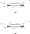
- Fig. 6 is a schematic diagram illustrating yet another modified implementation of the photosensitive assembly 710 according to an example of the present application, wherein in this modified implementation, a structural configuration of the circuit board main body 7111 is adjusted to change the manner of mounting the photosensitive chip 712 on the circuit board 711. Particularly, as shown in Fig. 6 , in this modified implementation, the lower surface of the circuit board 711 located around the through hole 7112 is recessed upward to form a groove 7117 communicating with the through hole 7112, wherein the circuit board electrical connecting terminal 7113 is disposed within the groove 7117.
- the photosensitive chip 712 when the lower surface of the circuit board 711 located around the through hole 7112 is recessed upward, the groove 7117 and the through hole 7112 form a receiving cavity 7118, and the photosensitive chip 712 is mounted in the receiving cavity 7118.
- the photosensitive chip 712 has a specific height, so that when the photosensitive chip 712 is mounted and electrically connected to the receiving cavity 7118 in the above-mentioned manner, the bottom surface of the photosensitive chip 712 is flush with the bottom surface of the circuit board 711, i.e., the photosensitive assembly 710 has a flat bottom surface.
- the photosensitive chip 712 may also have other height configurations.
- the photosensitive chip 712 has a specific height, so that when the photosensitive chip 712 is mounted and electrically connected in the receiving cavity 7118 in the above-mentioned manner, the bottom surface of the photosensitive chip 712 protrudes from the bottom surface of the circuit board 711.
- the bottom surface of the photosensitive chip 712 is lower than the bottom surface of the circuit board 711.
- the photosensitive assembly 710 further includes at least one electronic component 713 disposed on the circuit board 711. It should be understood that, in an example of the present application, since the photosensitive chip 712 is electrically connected to the lower surface of the circuit board 711, compared with the existing photosensitive assembly 710 packaged by the COB process, the upper surface of the circuit board 711 has a relatively larger area for mounting the electronic components 713.
- a relatively larger number of the electronic component 713 is disposed on the upper surface of the circuit board 711 (even all the electrical components are disposed on the upper surface of the circuit board 711), and a relatively small number of the electronic component 713 are disposed on the lower surface of the circuit board 711.
- the at least one electronic component 713 may also be all disposed on the lower surface of the circuit board 711; in this regard, it is not limited by the present application.
- the electronic component 713 includes capacitor, resistor, inductor, and the like.
- the packaging body 714 may be integrally formed on the lower surface of the circuit board 711 by a molding process or mold pressing process, wherein the packaging body 714 embeds at least a part of the lower surface of the circuit board 711, the lower surface and side surface of the photosensitive chip 712, and at least one electronic component 713 disposed on the lower surface of the circuit board 711.
- the size of the shielding case 715 is slightly larger than that of the photosensitive chip 712, so that after being disposed on the lower surface of the circuit board 711, the shielding case 715 completely accommodates the photosensitive chip 712 in the receiving cavity 7118 defined by itself, thereby preventing the photosensitive chip 712 from being interfered during the working process.
- the shielding case 715 may be bonded to the lower surface of the circuit board 711 by soldering, gluing, or the like.
- the photosensitive assembly 710 further includes a packaging body 714, wherein the packaging body 714 is integrally formed on the lower surface of the circuit board 711 and embeds at least a part of the lower surface of the circuit board 711, the shielding case 715, and at least a part of at least one electronic component 713 disposed on the lower surface of the circuit board 711.
- the packaging body 714 may be integrally formed on the lower surface of the circuit board 711 by a molding process or a mold pressing process, wherein the packaging body 714 embeds at least a part of the lower surface of the circuit board 711, the outer surface of the shielding case 715, and at least one electronic component 713 disposed on the lower surface of the circuit board 711.
- the shielding case 715 may effectively prevent the molding material or the mold pressing material from penetrating into the photosensitive area 7121 of the photosensitive chip 712, causing pollution to the photosensitive chip 712; at the same time, the shielding case 715 may also protect the photosensitive chip 712 from being directly contacted and/or impacted by the packaging material during the process of back surface packaging, or protect the photosensitive chip 712 from being directly affected by the pressing force from the mold, which has the function of protecting the photosensitive chip 712 from deformation, cracking and displacement.
- the shielding case 715 may also be disposed on the lower surface of the circuit board 711 in other ways.
- the size of the shielding case 715 corresponds to the size of the lower surface of the circuit board 711, wherein the shielding case 715 is mounted on the edge area of the circuit board 711 to cover the photosensitive chip 712 and the at least one electronic component 713 disposed on the lower surface of the circuit board 711.
- the photosensitive assembly 710 is not provided with the packaging body 714, since the shielding case 715 per se may realize the function of the packaging body 714.
- the shielding case 715 may not only create a good electromagnetic shielding environment for the photosensitive chip 712, but also may protect the lower surface of the circuit board 711, the photosensitive chip 712 mounted and electrically connected to the lower surface of the circuit board 711, and at least one electronic component 713 disposed on the lower surface of the circuit board 711.
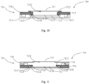
- Fig. 11 is a schematic diagram illustrating yet another modified implementation of the photosensitive assembly 710 according to an example of the present application.
- the photosensitive assembly 710 when the photosensitive chip 712 is mounted on the lower surface of the circuit board 711 in the manner as shown in Fig. 6 or Fig. 8 , and the at least one electronic component 713 is disposed on the upper surface of the circuit board 711, the photosensitive assembly 710 further includes a reinforcing plate 716 disposed on the lower surface of the circuit board 711.
- the photosensitive assembly 710 is not provided with the shielding case 715 and the packaging body 714, the reason is that: when the reinforcing plate 716 is mounted on the lower surface of the circuit board 711, the reinforcing plate 716 seals the receiving cavity 7118 formed by the groove 7117 of the circuit board main body 7111 and the through hole 7112, so as to seal the photosensitive chip 712 in the receiving cavity 7118, thereby creating a good, enclosed electromagnetic environment for the photosensitive chip 712. Meanwhile, the reinforcing plate 716 mounted on the lower surface of the circuit board 711 may effectively protect the lower surface of the circuit board 711.
- the reinforcing plate 716 is preferably implemented as a metal plate, so as to enhance the effect of heat dissipation.
- the reinforcing plate 716 may also be implemented as a plate of other materials, such as ceramics; in this regard, it is not limited by the present application.
- the photosensitive assembly 710 further includes a filter element 717 disposed on the upper surface of the circuit board 711 and corresponding to the through hole 7112, wherein the function of the filter element 717 is to filter the light entering the photosensitive chip 712.
- the filter element 717 is directly disposed on the upper surface of the circuit board 711, i.e., in an example of the present application, the photosensitive assembly 710 is not provided with a conventional bracket structure, thereby reducing the overall height of the photosensitive assembly 710 and/or the camera module.
- the filter element 717 may be implemented as different types, including but not limited to, the filter element 717 may be implemented as an infrared cut filter, a fully transparent spectral filter, and other filters or a combination of multiple filters.
- the filter element 717 when the filter element 717 is implemented as a combination of an infrared cut-off filter and a fully transparent spectral filter, i.e., the infrared cut-off filter and the fully transparent spectral filter may be switched to be selectively located on the photosensitive path of the photosensitive chip 712, so that the infrared cut-off filter may be switched to the photosensitive path of the photosensitive chip 712 when it is used in an environment with sufficient light such as during the day, thereby filtering the infrared rays in the light which is reflected by the object and enters into the photosensitive chip 712 by the infrared cut-off filter; in addition, when it is used in a dark environment such as night, the fully transparent spectral filter may be switched to the photosensitive path of the photosensitive chip 712, thereby allowing the infrared part of the light which is reflected by the object and enters into the photosensitive chip 712 to pass through the filter.
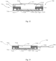
- Fig. 12 is a schematic diagram illustrating yet another modified implementation of the photosensitive assembly 710 according to an example of the present application.
- the photosensitive assembly 710 further includes a filter element bracket 718 disposed on the upper surface of the circuit board 711, wherein the filter element 717 is mounted on the upper surface of the filter element bracket 718.
- the filter element 717 may also be disposed at other positions of the camera module (for example, on the top side of the optical lens 720); in this regard, it is not limited by this application.
- the optical lens 720 is directly disposed on the upper surface of the circuit board 711, so that the overall height of the photosensitive assembly 710 and/or the camera module is further reduced.
- the optical lens 720 is mounted on the lens bracket.
- the reason why the optical lens 720 may be directly mounted on the upper surface of the circuit board 711 is that: the photosensitive chip 712 is disposed on the back side of the circuit board 711, and such a structural configuration may increase the optical back focal length of the camera module.
- the optical lens 720 may be implemented as an integral lens or a split lens (assembled from a plurality of lens parts); in this regard, it is not limited by the present application.
- Fig. 13 is a schematic diagram illustrating yet another modified implementation of the photosensitive assembly 710 according to an example of the present application.
- the photosensitive assembly 710 further includes a flexible board connecting plate 7191 electrically connected to the circuit board 711 and an electrical connector 7192 electrically connected to the flexible board connecting plate 7191, so as to realize the electrical connection between the camera module and/or the photosensitive assembly 710 and the external device through the electrical connector 7192.
- the flexible board connecting plate 7191 is integrally combined with the circuit board 711.
- the flexible board connecting plate 7191 is embedded into the circuit board main body 7111 (e.g., in the middle position) to be integrated with the circuit board 711.
- the flexible board connecting plate 7191 may also be combined with the circuit board 711 in other ways, for example, in another modified implementation of the photosensitive assembly 710 as shown in Fig. 14 , the flexible board connecting plate 7191 is mounted and electrically connected to the upper surface of the circuit board 711 through a conducting medium 7114 and a non-conducting adhesive 7115; for another example, in another modified implementation of the photosensitive assembly 710 as shown in Fig. 15 , the flexible board connecting plate 7191 is mounted and electrically connected to the lower surface of the circuit board 711; in this regard, it is not limited by this application.
- the photosensitive chip 712 in the photosensitive assembly 710 is electrically connected to the circuit board 711 by directly contacting the conducting medium 7114 disposed on the circuit board 711.
- the current configuration in which the photosensitive chip 712 and the circuit board 711 are electrically connected by wires is cancelled, so as to shorten the conduction distance, enhance the conductivity and signal transmission ability, and reduce the loss of the signal during the transmission process.
- the photosensitive chip 712 is electrically connected to the circuit board 711 by being pressed against the conducting medium 7114 disposed on the circuit board 711, and the photosensitive chip 712 is bonded to the circuit board 711 through the non-conducting adhesive 7115 disposed on the conducting medium 7114, thereby ensuring the stability of the electrical connection between the photosensitive chip 712 and the circuit board 711. That is to say, compared with the existing FC process, in an example of the present application, the photosensitive chip 712 realizes stable electrical connection between the photosensitive chip 712 and the circuit board 711 with relatively low cost and relatively low process difficulty.
- the photosensitive assembly 710 is at a relatively low temperature (about 80° to 150°). That is to say, in an implementation of the present application, the process of electrically connecting the photosensitive chip 712 to the circuit board 711 is performed at a relatively low temperature, so as to reduce the difficulty of the process on one hand, and on the other hand to reduce the amount of expansion and contraction of the non-conducting adhesive 7115 disposed between the photosensitive chip 712 and the circuit board 711, thereby reducing the deformability of the non-conducting adhesive 7115 to the photosensitive chip 712.
- the photosensitive chip 712 is disposed on the lower surface of the circuit board 711, and in an example of the present application, the filter element 717 may be directly disposed on the upper surface of the circuit board 711. That is to say, in an example of the present application, the photosensitive assembly 710 is not provided with a traditional bracket structure, so that the overall height of the photosensitive assembly 710 and/or the camera module may be reduced.
- the photosensitive chip 712 is disposed on the back side of the circuit board 711, and such a structural configuration may increase the optical back focal length of the camera module, so that it is still guaranteed that the camera module may be configured with an optical lens having a longer focal length, under the premise that the thickness of the camera module is reduced.
- the above camera module is exemplarily implemented as a fixed-focus camera module
- the camera module referred in the present application may also be implemented as a moving-focus camera module, i.e., the camera module further includes a driving element (not shown) disposed between the optical lens 720 and the photosensitive assembly 710, so as to carry the optical lens to move along the photosensitive path via the driving element, thereby changing the distance between the optical lens and the photosensitive assembly 710.
- the camera module referred in the present application may also be implemented as an optical anti-shake camera module, i.e., the camera module further includes an anti-shake motor (not shown) disposed between the optical lens 720 and the photosensitive assembly 710, thereby eliminating the influence of inadvertent shake during the shooting process on the image quality via the anti-shake motor; in this regard, it is not limited by this application.
- an anti-shake motor not shown
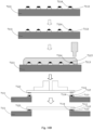
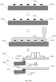
- a manufacturing process of the photosensitive assembly 710 according to an example of the present application is illustrated. And the manufacturing process as shown in Figs. 16A-16C is taken as an example of manufacturing the photosensitive assembly 710 as shown in Fig. 2 .
- the circuit board 711 includes a circuit board main body 7111, a through hole 7112 formed through the circuit board main body 7111, and a set of circuit board electrical connecting terminals 7113 disposed on a lower surface of the circuit board main body 7111.
- An upper surface of the photosensitive chip 712 includes a photosensitive area 7121, a non-photosensitive area 7121 located around the photosensitive area 7121, and a chip electrical connecting terminal 7122 disposed in the non-photosensitive area 7121.
- a conducting medium 7114 is formed on the electrical connecting terminals 7113 of the circuit board 711, respectively.
- forming a conducting medium 7114 on the circuit board electrical connecting terminal 7113 includes: firstly, providing a layer of mask 730 or a printing plate on the lower surface of the circuit board 711, wherein the mask 730 has a series of openings 7300 passing through it and corresponding to the circuit board electrical connecting terminals 7113 respectively; and applying excess conducting medium 7114 on the mask 730; then removing the redundant conducting medium 7114 from the surface of the mask 730; and then, removing the mask 730 to form the conducting medium 7114 at positions corresponding to the openings 7300.
- the size of the opening 7300 is smaller than that of the circuit board electrical connecting terminal 7113, so that the mask 730 is removed to form the conducting medium 7114 at the corresponding position of the opening 7300, wherein the conducting medium has the following properties: the size of the conducting medium 7114 is smaller than that of the circuit board electrical connecting terminal 7113, and the conducting medium 7114 covers a part of the circuit board electrical connecting terminal 7113.
- the size of the opening 7300 of the mask 730 may correspond to that of the circuit board electrical connecting terminal 7113, so that the mask 730 is removed to form the conducting medium 7114 at the corresponding position of the opening 7300, wherein the conducting medium has the following properties: the size of the conducting medium 7114 is equal to that of the circuit board electrical connecting terminal 7113, and the conducting medium 7114 completely covers the circuit board electrical connecting terminal 7113.
- the size of the opening 7300 of the mask 730 may be larger than that of the circuit board electrical connecting terminal 7113, so that the mask 730 is removed to form the conducting medium 7114 at the corresponding positions of the opening 7300, wherein the conducting medium has the following properties: the size of the conducting medium 7114 is larger than that of the circuit board electrical connecting terminal 7113, and the conducting medium 7114 covers the circuit board electrical connecting terminal 7113 therein.
- the conducting medium 7114 will become a conductive round convex shape with a structure of small upper part and big lower part due to the effect of gravity, and its upper surface is a cambered surface. Further, the conducting medium 7114 may be pre-cured by heating, so as to be fixed on the circuit board electrical connecting terminal 7113.
- a non-conducting adhesive 7115 is applied on the conducting medium 7114.
- the chip electrical connecting terminal 7122 is pressed against on the conducting medium 7114 to electrically connect the chip electrical connecting terminal 7122 and the circuit board electrical connecting terminal 7113, and the photosensitive chip 712 is bonded to the lower surface of the circuit board 711 via a non-conductive adhesive 7115; and in this way, the photosensitive chip 712 is electrically connected to the circuit board 711.
- the conducting medium 7114 and the non-conducting adhesive 7115 are configured to have the following properties: during the process of electrically connecting the photosensitive chip 712 to the circuit board 711, the photosensitive assembly 710 is heated to a specific temperature range, wherein the conducting medium 7114 has deformable property within the specific temperature range, and at the same time, the non-conducting adhesive 7115 is cured in this specific temperature range.
- the photosensitive chip 712 and the circuit board 711 are heated to 80°C-150°C; wherein the conducting medium 7114 has deformable property and at the same time the non-conducting adhesive 7115 is cured in this specific temperature range.
- the photosensitive chip 712 is brought close to the circuit board 711, so that the chip electrical connecting terminal 7122 of the photosensitive chip 712 corresponds to the circuit board electrical connecting terminal 7113 of the circuit board 711; further, the distance between the photosensitive chip 712 and the circuit board 711 is gradually shortened (for example, the photosensitive chip 712 is pressed down), so that the chip electrical connecting terminal 7122 of the photosensitive chip 712 passes through the incompletely cured non-conducting adhesive 7115 to contact the conducting medium 7114, thereby realizing the electrical connection between the photosensitive chip 712 and the circuit board 711; secondly, the distance between the photosensitive chip 712 and the circuit board 711 is continuously shortened (for example, continuing to press down the photosensitive chip
- the non-conducting adhesive 7115 will also be gradually cured, so that during the process of electrically connecting the photosensitive chip 712 to the lower surface of the circuit board 711, the photosensitive chip 712 is also firmly attached to the lower surface of the circuit board 711 via the non-conducting adhesive 7115.
- the stability of electrical connection between the photosensitive chip 712 and the circuit board 711 may be ensured; on the other hand, the bonding strength between the photosensitive chip 712 and the circuit board 711 may also be effectively ensured.
- the photosensitive chip 712 is electrically connected to the lower surface of the circuit board 711, and the photosensitive chip 712 is bonded to the lower surface of the circuit board 711 almost simultaneously, so that the physical bonding between the photosensitive chip 712 and the circuit board 711 via the non-conducting adhesive 7115 may ensure the stability of the electrical connection between the photosensitive chip 712 and the circuit board 711.
- a conductive film 7116 may also be formed on the surface of the conducting medium 7114, for example, by means of chemical coating or electroplating.
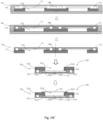
- the exemplary manufacturing process further includes: integrally forming a packaging body 714 on the lower surface of the circuit board 711, wherein the packaging body 714 embeds at least a part of the lower surface of the circuit board 711, the photosensitive chip 712, and at least a part of at least one electronic component 713 disposed on the lower surface of the circuit board 711.
- the component formed by the circuit board 711, the photosensitive assembly 710 and the at least one electronic component 713 is placed in a molding cavity 7400 of a molding die 740, and then the molding cavity 7400 is filled with molding material, after the molding material is cured and molded, the packaging body 714 is formed on the corresponding position of the lower surface of the circuit board 711.
- the packaging body 714 before the packaging body 714 is formed on the lower surface of the circuit board 711 through a molding process, it further includes: disposing a shielding case 715 on the lower surface of the circuit board 711, wherein the shielding case 715 covers the photosensitive chip 712 therein.
- a packaging body 714 is integrally formed on the lower surface of the circuit board 711, wherein the packaging body 714 is integrally formed on the lower surface of the circuit board 711 and embeds at least a part of the lower surface of the circuit board 711, the shielding case 715, and at least a part of at least one electronic component 713 disposed on the lower surface of the circuit board 711.
- an air escape channel may be disposed on the circuit board 711 to pass through it and communicate with the airtight chamber.
- the air escape channel needs to be resealed.
- the shielding case 715 when the size of the shielding case 715 corresponds to that of the lower surface of the circuit board 711, the shielding case 715 may be mounted on the edge area of the circuit board 711 to cover the photosensitive chip 712 and at least one electronic component 713 disposed on the lower surface of the circuit board 711. In this case, the photosensitive assembly 710 may not need to be provided with the packaging body 714.
- the shielding case 715 may be disposed on the lower surface of the circuit board 711, wherein the shielding case 715 covers the photosensitive chip 712 and the lower surface of the circuit board 711 therein.
- the manufacturing process further includes: mounting a reinforcing plate 716 on the lower surface of the circuit board 711, wherein the reinforcing plate 716 covers at least a part of the lower surface of the circuit board 711 and the photosensitive chip 712.
- it further includes: disposing a filter element 717 on the upper surface of the circuit board 711, wherein the filter element 717 corresponds to the through hole 7112 of the circuit board 711.
- the photosensitive chip 712 is mounted and electrically connected to the lower surface of the circuit board 711, and then the filter element 717 is mounted on the upper surface of the circuit board 711, before the filter element 717 is mounted, the photosensitive area 7121 of the photosensitive chip 712 of the photosensitive chip 712 is exposed, and no effective isolation measures are provided, thus the photosensitive area 7121 may be contaminated by dirty substance such as dust, or scratched by sharp objects.
- an isolation layer e.g., an adhesive layer
- an isolation layer may be applied on at least the photosensitive area 7121 of the photosensitive chip 712 in advance, thereby preventing the photosensitive chip 712 from being contaminated or scratched.
- the isolation layer (for example, when the isolation layer is an adhesive layer, the isolation layer may be removed by washing with water or dissolving with an organic solvent) is removed, and then the filter element 717 is mounted again.
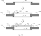
- the filter element 717 may also be mounted on the upper surface of the circuit board 711 optionally, so that when the photosensitive chip 712 is attached and electrically connected to the lower surface of the circuit board 711 through the above-mentioned manufacturing process, the photosensitive area 7121 of the photosensitive chip 712 is located in a closed chamber surrounded by the filter element 717, the circuit board 711 and the photosensitive chip 712, thereby preventing the photosensitive chip 712 from being contaminated or scratched.
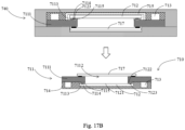
- Figs. 17A-17B such an exemplary process is illustrated in Figs. 17A-17B .
- the filter element 717 is mounted on the upper surface of the circuit board 711;
- the photosensitive chip 712 is mounted and electrically connected to the lower surface of the circuit board 711 through the manufacturing process mentioned above, so that the photosensitive area 7121 of the photosensitive chip 712 is located in an airtight chamber surrounded by the filter element 717, the circuit board 711 and the photosensitive chip 712, thereby preventing the photosensitive chip 712 from being contaminated or scratched;
- the shielding case 715 is mounted on the lower surface of the circuit board 711;
- the molded body is formed on the lower surface of the circuit board 711 through a molding process.
- the photosensitive assembly 710 may be prepared in a manner of jointed panel manufacturing, i.e., the circuit board 711 is implemented as a jointed panel of the circuit board 711, and includes at least two monomers of the circuit board 711.
- the flexible board connecting plate 7191 and the electrical connector 7192 may also be pre-configured on the circuit board 711; in this regard, it should be easily understood by those of ordinary skill in the art.
- the electrical connection between the hard board and the flexible board in the circuit board of the camera module is realized by ACF (Anisotropic Conductive Film).
- ACF Advanced Conductive Film
- the electrical connecting structure formed by the hard board and the flexible board has certain defects, such as uncontrollable electrical conduction performance, high process temperature, and excessive pressing force.
- Fig. 18 is a schematic diagram illustrating the structure of a conventional ACF.
- ACF mainly includes resin adhesive and conductive particles, and its conduction principle is: electrically connecting the electrical connecting terminals of the hard board and the flexible board via conductive particles, and at the same time avoiding the short circuit of the adjacent electrical connecting terminals, thereby achieving the purpose of conduction only in the Z-axis direction. That is to say, ACF may realize that the resistance characteristics of the Z-axis electrical conduction direction and the XY insulation plane are significantly different; when the difference between the conducting resistance value in the Z-axis direction and the insulating resistance value of the XY plane exceeds a certain ratio, it may be called good conductivity and anisotropy.
- the anisotropic conductive properties mainly depend on the filling rate of the conductive particles.
- the conductivity of ACF will be increased with the increase of the filling rate of conductive particles, at the same time, the probability of short circuit caused by contacting each other between the conductive particles will also be increased.
- the particle size distribution and distribution uniformity of the conductive particles will also affect the anisotropic conductive properties.
- conductive particles must have good particle size uniformity and roundness to ensure consistent contact area between electrodes and conductive particles, thereby maintaining the same conducting resistance, and at the same time avoiding some electrodes not contacting conductive particles to result in an open circuit.
- the common particle size range is 3-5 ⁇ m, too large conductive particles will reduce the number of particles in contact with each electrode, and at the same time, it is easy to cause contact between the conductive particles of adjacent electrodes and result in short circuit; too small conductive particles are easy to cause the problem of particle aggregation and result in uneven particle distribution density.
- the conductive particles are mainly metal powders and polymer plastic ball coated with metal. Commonly used metal powders include nickel (Ni), gold (Au), gold plating on nickel, silver and tin alloy.
- the conductive particles in the ACF are uniformly distributed in the binder and do not contact each other, i.e., the ACF film is non-conducting in the non-usage state.
- the ACF film is pressurized and heated; typically, the pressurizing and heating are performed in two times, the first time is for pre-positioning with a heating temperature of 60-100°C and a pressure of (3-10) ⁇ 10 4 Pa, and the second time is for fixing with a heating temperature of about 150-200°C and a pressure of (20-40) ⁇ 10 4 Pa.
- the insulating film of the conductive particles is ruptured and squeezed together in the part having the circuit to result in conduction.
- the gaps of the upper and lower electrical connecting terminals are filled with fluidity by ACF, similarly the gaps of the upper and lower electrical connecting terminals are filled with fluidity by the conductive particles in the ACF.
- the conductive particles may flow into the gap, and the accuracy is not very controllable; in the other hand, there are also conductive particles exist between the lateral electrical connecting terminals, excessive or large conductive particles may contact and connect with each other between adjacent lateral electrical connecting terminals during the pressing process, resulting in a short circuit of lateral conduction and abnormal electrical function.
- the pressing force required in this process is large, and the process is difficult.
- the temperature required in this process is high (the temperature of the second heating is about 150-200°C), and an excessively high temperature will cause a large amount of expansion and contraction of the hard board, resulting in bending of the hard board.
- the basic idea of the present application is to provide an integral connecting structure, which includes a conducting medium and a non-conducting adhesive adjacent to each other, so as to realize the electrical connection between the circuit board main body and the electrical connecting plate through the integral connecting structure.
- the present application provides a circuit board assembly, which includes a circuit board main body, an electrical connecting plate, and an electrical connector.
- the circuit board main body has a circuit board electrical connecting terminal disposed on the surface thereof.
- the electrical connecting plate has a connecting plate electrical connecting terminal disposed on the surface thereof and corresponding to the circuit board electrical connecting terminal.
- the circuit board assembly further includes an integral connecting structure disposed between the connecting plate electrical connecting terminal and the circuit board electrical connecting terminal.
- the integral connecting structure includes a conducting medium and a non-conducting adhesive adjacent to each other, wherein the connecting plate electrical connecting terminal is electrically connected to the circuit board electrical connecting terminal via the conducting medium, while the electrical connecting plate is bonded to the circuit board via the non-conducting adhesive. In this way, conduction between the circuit board main body and the electrical connecting plate is achieved through the integral connecting structure and the corresponding electrical conduction process.
- the circuit board assembly 810 is a circuit board assembly for a camera module, which includes a circuit board main body 811, and the electrical connecting plate 812 electrically connected to the circuit board main body 811, and an electrical connector 813 electrically connected to the electrical connecting plate 812, wherein the electrical connector 813 is used to conduct the camera module and other electrical components.
- the electrical connecting plate 812 is electrically connected to the circuit board main body 811 through an integral connecting structure 8110.
- the circuit board main body 811 is generally implemented as a hard board, which includes a set of circuit board electrical connecting terminals 8113 disposed on the surface thereof.
- the electrical connecting plate 812 is generally implemented as a flexible board, which includes a connecting plate electrical connecting terminal 8122 disposed on the surface thereof, wherein the connecting plate electrical connecting terminals 8122 correspond to the circuit board electrical connecting terminal 8113.
- the integral connecting structure 8110 is formed on the circuit board main body 811, wherein the conducting medium 8114 is formed on the circuit board electrical connecting terminal 8113, the non-conducting adhesive 8115 is applied to the conducting medium 8114 to form the integral connecting structure 8110.
- the electrical connecting plate 812 is pressed against the integral connecting structure 8110, so that the connecting plate electrical connecting terminal 8113 is electrically connected to the circuit board main body 811 via the conducting medium 8114, while the electrical connecting plate 812 is bonded to the circuit board main body 811 via the non-conducting adhesive 8115.
- the physical bonding between the circuit board main body 811 and the electrical connecting plate 812, and the electrical connection between the circuit board main body 811 and the electrical connecting plate 812 are synchronized and realized through the integral connecting structure 8110.
- the integral connecting structure 8100 is used as a medium for integration, thereby synchronously realizing the electrical connection and the non-electrical connection between the electrical connecting plate 812 and the circuit board 811.
- Such a process may simultaneously take into account the bonding strength of the electrical connecting plate 812 and the circuit board main body 811, and the stability of the electrical connection between the electrical connecting plate 812 and the circuit board main body 811. It is worth mentioning that, such a process may also be carried out at relatively low temperatures and requires only relatively small pressing force.
- the key point to the implementation of this process is that: there is a special relationship between the properties of the conducting medium 8114 and the non-conducting adhesive 8115 in the integral connecting structure 8110.
- the conducting medium 8114 and the non-conducting adhesive 8115 are configured to have the following properties: during the process of electrically connecting the electrical connecting plate 812 to the circuit board main body 811, the circuit board assembly 810 is heated to a specific temperature range, wherein the conducting medium 8114 has deformable property in such specific temperature range, and at the same time, the non-conducting adhesive 8115 will be cured in this specific temperature range.
- the connecting plate electrical connecting terminal 8122 of the electrical connecting plate 812 may pass through the non-conducting adhesive 8115 that is not fully cured to be in contact with the conducting medium 8114, and is electrically connected to the circuit board electrical connecting terminal 8113 of the circuit board main body 811 in this way, at the same time the non-conducting adhesive 8115 is also slowly cured, so that after the electrical connecting plate 812 is electrically connected to the lower surface of the circuit board main body 811, the electrical connecting plate 812 is also firmly attached to the lower surface of the circuit board main body 811 via the non-conducting adhesive 8115.
- the non-conducting adhesive 8115 includes a resin material such as epoxy resin or polyimide resin, which will be cured in a temperature range of 80-200°C.
- the circuit board assembly 810 is heated to a specific temperature range, preferably, the specific temperature range is 80 °C-150°C.
- the conducting medium 8114 includes an adhesive with flexible characteristics, and the non-conducting adhesive 8115 also has good flexibility.
- the integral connecting structure 8110 has a deformable property, which facilitates the electrical connecting plate 812 to synchronously realize the electrical connection and non-electrical connection between the electric connecting plate 812 and the circuit boards 811 in a manner of pressing the electric connecting plate 812 against the integral connecting structure 8110.
- the required pressing force is 0.5-5N.
- the electrical connection and the non-electrical connection between the electrical connecting plate 812 and the circuit board main body 811 may be realized simultaneously with a relatively small pressing force, and the process difficulty is lower; in addition, the low pressing force may also protect the electrical connecting plate 812 to avoid being deformed, broken, and other undesirable phenomena; while in the existing FC process, the pressing force is usually above 10N (usually is set to 30N), and the pressing force is relatively large, the photosensitive chip is at risk of being deformed or even broken.
- the circuit board assembly 810 is heated to a relatively low temperature (at 80-150°).
- the process of electrically connecting the electrical connecting plate 812 to the circuit board main body 811 is performed at a relatively low temperature, so that the difficulty of the process is reduced on one hand; and on the other hand, the amount of expansion and contraction of the non-conducting adhesive 8115 disposed between the electrical connecting plate 812 and the circuit board main body 811 is also reduced, thereby reducing the deformability of the non-conducting adhesive 8115 on the circuit board main body 811 and the electrical connecting plate 812, and improving the flatness of the circuit board main body 811 and the electrical connecting plate 812.
- the process of electrically connecting the electrical connecting plate 812 to the circuit board main body 811 is performed at a relatively low temperature, the self-expansion of the circuit board main body 811 will be relatively reduced, thereby facilitate to improve the surface flatness of the circuit board main body 811.
- the conducting medium 8114 is disposed on the circuit board electrical connecting terminal 8113 of the circuit board main body 811, wherein the conducting medium 8114 has a circular convex shape (the reason for having such a shape is the surface tension of the conducting medium 8114).
- the size of the conducting medium 8114 is smaller than that of the circuit board electrical connecting terminal 8113, and the conducting medium 8114 covers a part of the circuit board electrical connecting terminal 8113, such a configuration of size relationship may effectively control the conducting medium 8114 within the range of the circuit board electrical connecting terminal 8113, so as to prevent the conducting medium 8114 from overflowing to contaminate the structure of the circuit board main body 811, during the process of electrically connecting the electrical connecting plate 812 to the circuit board main body 811.
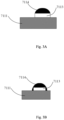
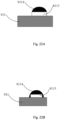
- the size relationship between the conducting medium 8114 and the circuit board electrical connecting terminal 8113 may also be configured in other types, for example, the size of the conducting medium 8114 is equal to that of the circuit board electrical connecting terminal 8113, and the conducting medium 8114 completely covers the circuit board electrical connecting terminal 8113 (as shown in Fig. 22A ); alternatively, the size of the conducting medium 8114 is larger than that of the circuit board electrical connecting terminal 8113, and the conducting medium 8114 covers the circuit board electrical connecting terminal 8113 therein (as shown in Fig. 22B ); in this regard, it is not limited by this application.
- the contact area between the conductive medium 8114 and the circuit board electrical connecting terminal 8113 may be increased, thereby improving the electrical conductivity.
- the contact area between the conducting medium 8114 and the circuit board electrical connecting terminal 8113 may be maximized, thereby further improving the electrical conductivity.
- the conducting medium 8114 when the size of the conducting medium 8114 is larger than that of the circuit board electrical connecting terminal 8113, and the conducting medium 8114 covers the circuit board electrical connecting terminal 8113 therein, it is necessary to control the distance between each of the conducting mediums 8114 disposed on the different circuit board electrical connecting terminals 8113, thereby preventing the circuit from being short-circuit and failing.
- the non-conducting adhesive 8115 is further applied on the conducting medium 8114, and preferably completely covers the conducting medium 8114 and the circuit board electrical connecting terminals 8113.
- the conducting medium 8114 and the non-conducting adhesive 8115 have a layered structure, i.e., the conducting medium 8114 and the non-conducting adhesive 8115 are not mixed with each other.
- the conductive particles are uniformly distributed in the adhesive (i.e., the conductive particles and the adhesive are mixed with each other); in addition, during the process of electrical connection between the hard board and the flexible board via ACF glue, the ACF glue is heated and pressurized to rupture the insulating film of the conductive particles to form conduction.
- the metal particles in the conducting medium 8114 are stacked, and the circuit board electrical connecting terminal 8113 of the circuit board main body 811 and the connecting plate electrical connecting terminal 8122 of the electric circuit board 812 are in contact with the metal particles in the conducting medium in both vertical and horizontal directions. In this way, the electrical conductivity between the circuit board main body 811 and the electrical connecting plate 812 is improved (especially conduction rate in the vertical direction).
- the gaps of the upper and lower electrical connecting terminals are filled with fluidity by ACF, similarly the gaps of the upper and lower electrical connecting terminals are filled with fluidity by the conductive particles in the ACF.
- the conductive particles may flow into the gap, and the accuracy is not very controllable; in the other hand, there are also conductive particles exist between the lateral electrical connecting terminals, excessive or large conductive particles may contact and connect with each other between adjacent lateral electrical connecting terminals during the pressing process, resulting in a short circuit of lateral conduction and abnormal electrical function.
- the non-conducting adhesive 8115 in the integral connecting structure 8110 covers the circuit board electrical connecting terminal 8113 and the conducting medium 8114, so that two adjacent circuit board electrical connecting terminals 8113 are blocked by the non-conducting adhesive 8115, thereby preventing a short circuit between the two circuit board electrical connecting terminals 8113.
- Fig. 23 is a schematic diagram illustrating a process of electrically connecting the electrical connecting plate 812 to the circuit board main body 811 according to an example of the present application.
- the temperature of the process environment is raised to 80-150°C
- firstly the electrical connecting plate 812 is brought close to the circuit board main body 811, so that the connecting plate electrical connecting terminal 8122 of the electrical connecting plate 812 corresponds to the circuit board electrical connecting terminal 8113 of the circuit board main body 811; secondly the distance between the electrical connecting plate 812 and the circuit board main body 811 is slowly reduced (for example, pressing down the electrical connecting plate 812), so that the connecting plate electrical connecting terminal 8122 of the electrical connecting plate 812 passes through the non-conducting adhesive 8115 that is not fully cured to be in contact with the conducting medium 8114, so as to realize the electrical connection between the electrical connecting plate 812 and the circuit board main body 811, and the conducting medium 8114 has
- the non-conducting adhesive 8115 will also be gradually cured, so that during the process of electrically connecting the electrical connecting plate 812 to the circuit board main body 811, the electrical connecting plate 812 is also firmly attached to the circuit board main body 811 via the non-conducting adhesive 8115.
- the stability of the electrical connection between the electric connecting plate 812 and the circuit board main body 811 may be ensured, and on the other hand the bonding strength between the electrical connecting plate 812 and the circuit board main body 811 may also be effectively ensured.
- the electrical connecting plate 812 is electrically connected to the circuit board main body 811, and the electrical connecting plate 812 is bonded to the circuit board main body 811 almost simultaneously, so that the physical bonding between the electrical connecting plate 812 and the circuit board main body 811 formed through the non-conducting adhesive 8115 may ensure the stability of the electrical connection between electrical connecting plate 812 and the circuit board main body 811.
- the conducting medium 8114 further includes a conductive film 8116 formed on the surface thereof.
- the conductive film 8116 completely covers the outer surface of the conducting medium 8114.
- the conductive film 8116 may be formed on the surface of the conducting medium 8114 by chemical plating or electroplating, wherein the coating material may be selected from gold, silver, aluminum, copper, and the like.
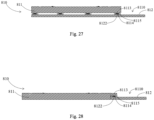
- the circuit board electrical connecting terminal 8113 is formed on the upper surface of the circuit board main body 811, more particularly, formed on an edge area of the upper surface; the connecting plate electrical connecting terminal 8122 is formed on the lower surface of the electrical connecting plate 812, more particularly, formed on an edge area of the lower surface thereof. That is to say, in an example of the present application, the electrical connecting plate 812 is mounted and electrically connected to the upper surface of the circuit board main body 811.
- the bonding position between the electrical connecting plate 812 and the circuit board main body 811 may also be implemented in other types.
- the edge area of the upper surface of the circuit board main body 811 is recessed downward to form a concave part, and the electrical connecting plate 812 is mounted and electrically connected to the concave part of the circuit board main body 811.
- the upper surface of the electrical connecting plate 812 is flush with the upper surface of the circuit board main body 811.
- the electrical connecting plate 812 is mounted and electrically connected to the lower surface of the circuit board main body 811. More particularly, in the modified implementation of the circuit board assembly as shown in Fig.
- the circuit board electrical connecting terminal 8113 is formed on the edge area of the lower surface of the circuit board main body 811, and the connecting plate electrical connecting terminals 8122 is formed on the edge area of the upper surface of the electrical connecting plate 812.
- the circuit board electrical connecting terminal 8113 is formed on the lower surface of the circuit board main body 811, and the connecting plate electrical connecting terminal 8122 is formed on the upper surface of the electrical connecting plate 812.
- the edge area of the lower surface of the circuit board main body 811 is recessed upward to form a concave part, and the electrical connecting plate 812 is mounted and electrically connected to the concave part of the circuit board main body 811, and preferably the lower surface of the electrical connecting plate 812 is flush with the lower surface of the circuit board main body 811.
- circuit board assembly 810 according to the examples of the present application has been illustrated, which has at least the following advantages.
- the electrical connection and the non-electrical connection between the circuit board main body 811 and the electrical connecting plate 812 is synchronously realized through the integral connecting structure 8110 composed of the conducting medium 8114 and the non-conducting adhesive 8115 which are disposed between the circuit board main body 811 and the electrical connecting plate 812. In this way, the stability of the electrical connection between the circuit board main body 811 and the electrical connecting plate 812 is improved.
- the conducting medium 8114 in the integral connecting structure 8110 is in contact with the circuit board main body 811 and the electrical connecting plate 812 in both vertical and horizontal directions, thereby improving the electrical conductivity (especially the conductivity in the vertical direction).
- the pressing force required for pressing the electrical connecting plate 812 against the circuit board main body 811 is relatively small, about 0.5-5N. That is to say, in an example of the present application, the electrical connection and the non-electrical connection between the circuit board main body 811 and the electrical connecting plate 812 may be realized simultaneously with a small pressing force, and the process difficulty is lower.
- the circuit board assembly 810 is heated to a relative low temperature (at 80-150°).
- the process of electrically connecting the electrical connecting plate 812 to the circuit board main body 811 is performed at a relatively low temperature, so as to reduce the difficulty of the process on one hand; and on the other hand the amount of expansion and contraction of the non-conducting adhesive 8115 disposed between the circuit board main body 811 and the electrical connecting plate 812 is reduced, thereby reducing the deformability of the non-conducting adhesive 8115 to the circuit board main body 811, and improving the flatness of the circuit board main body 811.
- the non-conducting adhesive 8115 in the integral connecting structure 8110 covers the circuit board electrical connecting terminal 8113 and the conducting medium 8114, so that two adjacent circuit board electrical connecting terminals 8113 are isolated by the non-conducting adhesive 8115, thereby preventing a short circuit between the two circuit board electrical connecting terminals 8113.
- integral connecting structure 8110 formed on the circuit board main body 811 is taken as an example and described above, those skilled in the art should know that in other examples of the present application, firstly the integral connecting structure 8110 may also be formed on the electrical connecting plate 812, i.e., the conducting medium 8114 is formed on the connecting plate electrical connecting terminal 8122, and the non-conducting adhesive 8115 is applied to the conducting medium 8114 to form the integral connecting structure 8110.
- the circuit board main body 811 is pressed against the integral connecting structure 8110 which is formed on the electrical connecting plate 812, so that the circuit board electrical connecting terminals 8113 is electrically connected to the connecting plate electrical connecting terminal 8122 via the conducting medium 8114, while the circuit board main body 811 is bonded to the electrical connecting plate 812 by the non-conducting adhesive 8115; in this regard, it is not limited by this application.
- circuit board assembly 810 as shown in Figs. 21-28 , it is only illustrated that the circuit board assembly 810 includes the circuit board main body 811, the electrical connecting plate 812 and the electrical connecting terminal 813, a person of ordinary skill in the art should know that in an actual product, the circuit board assembly 810 further includes at least one electronic component (e.g., capacitor, inductor, resistor, etc.) disposed on the circuit board main body 811; in this regard, it is not limited by this application.
- at least one electronic component e.g., capacitor, inductor, resistor, etc.
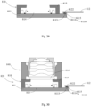
- the circuit board assembly 810 may cooperate with other components to form a photosensitive assembly 820, wherein the photosensitive assembly 820 includes the circuit board assembly 810 described above and a photosensitive chip 814 electrically connected to the circuit board main body 811, and other necessary components, such as a packaging body 815 formed on the circuit board main body 811, a filter element 816 supported on the photosensitive chip 814, etc., since it is not the focus of this application, it will not be repeated herein.
- the photosensitive assembly 820 may also cooperate with an optical lens 840 to form a camera module, wherein the optical lens 840 is maintained in the photosensitive path of the photosensitive assembly 820.
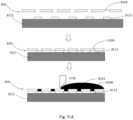
- FIGs. 31A-31B the first manufacturing process of the circuit board assembly according to an example of the present application is illustrated, wherein the manufacturing process as shown in Figs. 31A-31B is taken as an example for manufacturing the circuit board assembly 810 as shown in Fig. 21 .
- a circuit board main body 811 and an electrical connecting plate 812 are provided, wherein the circuit board main body 811 has circuit board electrical connecting terminals 8113 disposed on the surface thereof, and the electrical connecting plate 812 has connecting plate electrical connecting terminals 8122 disposed on the surface thereof.
- a conductive medium 8114 are formed on the circuit board electrical connecting terminals 8113 respectively.
- a conducting medium 8114 on the circuit board electrical connecting terminals 8113 including: Firstly, a layer of mask 830 or a printing plate is disposed on the upper surface of the circuit board main body 811, wherein the mask 830 has a series of openings 8300 passing through it and corresponding to the circuit board electrical connecting terminals 8113 respectively. Then, excess conducting medium 8114 is applied over the mask 830. Next, the redundant conducting medium 8114 on the surface of the mask 830 is removed. Then, the mask 830 is removed to form the conducting medium 8114 at positions corresponding to the openings 8300.
- the size of the opening 8300 is smaller than that of the circuit board electrical connecting terminal 8113, so that the mask 830 is removed to form the conducting medium 8114 at the corresponding position of the opening 8300, wherein the conducting medium has the following properties: the size of the conducting medium 8114 is smaller than that of the circuit board electrical connecting terminal 8113, and the conducting medium 8114 covers a part of the circuit board electrical connecting terminal 8113.
- the size of the opening 8300 of the mask 830 may correspond to that of the circuit board electrical connecting terminal 8113, so that the mask 830 is removed to form the conducting medium 8114 at the corresponding position of the opening 8300, wherein the conducting medium has the following properties: the size of the conducting medium 8114 is equal to that of the circuit board electrical connecting terminal 8113, and the conducting medium 8114 completely covers the circuit board electrical connecting terminal 8113.
- the size of the opening 8300 of the mask 830 may be larger than that of the circuit board electrical connecting terminal 8113, so that the mask 830 is removed to form the conducting medium 8114 at the corresponding position of the opening 8300, wherein the conducting medium has the following properties: the size of the conducting medium 8114 is larger than that of the circuit board electrical connecting terminal 8113, and the conducting medium 8114 covers the circuit board electrical connecting terminal 8113 therein.
- the conducting medium 8114 will become a conductive round convex with a structure of small upper part and big lower part due to the effect of gravity, and its upper surface is a cambered surface. Further, the conducting medium 8114 may be pre-cured by heating, so as to be fixed on the circuit board electrical connecting terminal 8113.
- a non-conducting adhesive 8115 is applied on the conducting medium 8114.
- the connecting plate electrical connecting terminal 8122 is pressed against the conducting medium 8114 to electrically connect the connecting plate electrical connecting terminal 8122 and the circuit board electrical connecting terminal 8113, and the electrical connecting plate 812 is bonded to the lower surface of the circuit board main body 811 through the non-conducting adhesive 8115, and in this way the electrical connecting plate 812 is electrically connected to the circuit board main body 811.
- the electrical connection and the non-electrical connection between the electrical connecting plate 812 and the circuit board main body 811 are realized through an integral connecting structure 8110 formed by the conducting medium 814 and the non-conducting adhesive 815 which are disposed between the circuit board main body 811 and the electrical connecting plate 812, thereby ensuring the stability of the electrical connection between the electrical connecting plate 812 and the circuit board main body 811, and reducing the process difficulty.
- the conducting medium 8114 and the non-conducting adhesive 8115 are configured to have the following properties: during the process of electrically connecting the electrical connecting plate 812 to the circuit board main body 811, the circuit board assembly 810 is heated to a specific temperature range, wherein the conducting medium 8114 has deformable property in this specific temperature range, and at the same time, the non-conducting adhesive 8115 is cured in this specific temperature range.
- the electrical connecting plate 812 and the circuit board main body 811 are heated to 80-150°C; in this temperature range, the conducting medium 8114 has deformable property, and at the same time the non-conducting adhesive 8115 is cured.
- the circuit board assembly 810 is heated to a relatively low temperature (at 80-150°). That is to say, in an example of the present application, the process of electrically connecting the electrical connecting plate 812 to the circuit board main body 811 is performed at a relatively low temperature.
- the electrical connecting plate 812 is brought close to the circuit board main body 811, so that the connecting plate electrical connecting terminals 8122 of the electrical connecting plate 812 correspond to the circuit board electrical connecting terminals 8113 of the circuit board main body 811; secondly the distance between the electric connecting plate 812 and the circuit board main body 811 is gradually shortened (for example, pressing down the electrical connecting plate 812), so that the connecting plate electrical connecting terminals 8122 of the electrical connecting plate 812 pass through the non-conducting adhesive 8115 that is not fully cured to be in contact with the conducting medium 8114, thereby achieving the electrical connection between the electrical connecting plate 812 and the circuit board main body 811; then the distance between the electrical connecting plate 812 and the circuit
- the non-conducting adhesive 8115 will be gradually cured, so that during the process of electrically connecting the electrical connecting plate 812 to the upper surface of the circuit board main body 811, the electrical connecting plate 812 is also firmly attached to the upper surface of the circuit board main body 811 via the non-conducting adhesive 8115.
- the stability of electrical connection between the electrical connecting plate 812 and the circuit board main body 811 may be ensured on one hand, and on the other hand the bonding strength between the electrical connecting plate 812 and the circuit board main body 811 may also be effectively ensured.
- electrically connecting the electrical connecting plate 812 to the upper surface of the circuit board main body 811, and bonding the electrical connecting plate 812 to the upper surface of the circuit board main body 811 are performed almost simultaneously, so that the physical bonding between the electrical connecting plate 812 and the circuit board main body 811 formed by the non-conducting adhesive 8115 may ensure the stability of the electrical connection between the electrical connecting plate 812 and the circuit board main body 811.
- the required pressing force is 0.5-5N. That is to say, in the present application, the electrical connection and the non-electrical connection between the electrical connecting plate 812 and the circuit board main body 811 may be realized simultaneously with a relatively small pressing force, and the process difficulty is lower; in addition, the low pressing force may also protect the electrical connecting plate 812 to avoid being deformed, broken and other undesirable phenomena; while in the existing FC process, the pressing force is usually above 10N (usually is set to 30N), and the pressing force is relatively large, so that the photosensitive chip is at risk of being deformed or even broken.
- a conductive film 8116 may also be formed on the surface of the conducting medium 8114, for example, by chemical plating or electroplating.
- FIG. 32A and Fig. 32B the second manufacturing process of the circuit board assembly according to an example of the present application is illustrated, wherein the manufacturing process as shown in Fig. 32A and Fig. 32B is taken as an example for manufacturing the circuit board assembly 810 as shown in Fig. 21 .
- a circuit board main body 811 and an electrical connecting plate 812 are provided, wherein the circuit board main body 811 has circuit board electrical connecting terminals 8113 disposed on the surface thereof, and the electrical connecting plate 812 has connecting plate electrical connecting terminals 8122 disposed on the surface thereof.
- a conductive medium 8114 are formed on the connecting plate electrical connecting terminals 8122 respectively.
- a conducting medium 8114 on the connecting plate electrical connecting terminals 8122 including: Firstly, a layer of mask 830 or a printing plate is disposed on the lower surface of the electrical connecting plate 812, wherein the mask 830 has a series of openings 8300 passing through it and corresponding to the connecting plate electrical connecting terminals 8122 respectively. Then, excess conducting medium 8114 is applied over the mask 830. Next, the redundant conducting medium 8114 on the surface of the mask 830 is removed. Then, the mask 830 is removed to form the conducting medium 8114 at positions corresponding to the openings 8300.
- the size of the opening 8300 is smaller than that of the connecting plate electrical connecting terminal 8122, so that the mask 830 is removed to form the conducting medium at the corresponding position of the opening 8300, wherein the conducting medium 8114 has the following properties: the size of the conducting medium 8114 is smaller than that of the connecting plate electrical connecting terminal 8122, and the conducting medium 8114 covers a part of the connecting plate electrical connecting terminal 8122.
- the size of the opening 8300 of the mask 830 may correspond to that of the connecting plate electrical connecting terminal 8122, so that the mask 830 is removed to form the conducting medium 8114 at the corresponding position of the opening 8300, wherein the conducting medium 8114 has the following properties: the size of the conducting medium 8114 is equal to that of the connecting plate electrical connecting terminal 8122, and the conducting medium 8114 completely covers the connecting plate electrical connecting terminal 8122.
- the size of the opening 8300 of the mask 830 may be larger than that of the connecting plate electrical connecting terminal 8122, so that the mask 830 is removed to form the conducting medium 8114 at the corresponding position of the opening 8300, wherein the conducting medium 8114 has the following properties: the size of the conducting medium 8114 is larger than that of the connecting plate electrical connecting terminal 8122, and the conducting medium 8114 covers the connecting plate electrical connecting terminal 8122 therein.
- the conducting medium 8114 will become a conductive round convex with a structure of small upper part and big lower part due to the effect of gravity, and its upper surface is a cambered surface. Further, the conducting medium 8114 may be pre-cured by heating, so as to be fixed on the connecting plate electrical connecting terminals 8122.
- a non-conducting adhesive 8115 is applied on the conducting medium 8114.
- the circuit board electrical connecting terminals 8113 are pressed against the conducting medium 8114 to electrically connect the circuit board electrical connecting terminals 8113 to the connecting plate electrical connecting terminals 8122, and the circuit board main body 811 is bonded to the lower surface of the electrical connecting plate 812 through the non-conducting adhesive 8115, and in this way the electrical connecting plate 812 is electrically connected to the circuit board main body 811.
- the electrical connection and non-electrical connection between the electrical connecting plate 812 and the circuit board main body 811 are realized through an integral connecting structure 8110 formed by the conducting medium 814 and the non-conducting adhesive 815 which are disposed between the circuit board main body 811 and the electrical connecting plate 812, thereby ensuring the stability of electrical connection between the electrical connecting plate 812 and the circuit board main body 811, and reducing the process difficulty.
- the conducting medium 8114 and the non-conducting adhesive 8115 are configured to have the following properties: during the process of electrically connecting the electrical connecting plate 812 to the circuit board main body 811, the circuit board assembly 810 is heated to a specific temperature range, wherein the conducting medium 8114 has deformable property in this specific temperature range, and at the same time the non-conducting adhesive 8115 is cured in this specific temperature range.
- the electrical connecting plate 812 and the circuit board main body 811 are heated to 80-150°C; in this temperature range, the conducting medium 8114 has deformable property, and at the same time the non-conducting adhesive 8115 will be cured.
- the circuit board assembly 810 is heated to a relatively low temperature (at 80-150°). That is to say, in an example of the present application, the process of electrically connecting the circuit board main body 811 to the electrical connecting plate 812 is performed at a relatively low temperature.
- the circuit board main body 811 is brought close to the electrical connecting plate 812, so that the circuit board electrical connecting terminals 8113 of the circuit board main body correspond to the connecting plate electrical connecting terminals 8122 of the electrical connecting plate 812; secondly the distance between the electrical connecting plate 812 and the circuit board main body 811 is gradually shortened (for example, pressing down the electrical connecting plate 812), so that the circuit board electrical connecting terminals 8113 of the circuit board main body 811 pass through the non-conducting adhesive 8115 that is not fully cured to be in contact with the conducting medium 8114, thereby realizing the electrical connection between the electrical connecting plate 812 and the circuit board main body 811; then the distance between the electrical connecting plate 812 and the circuit board main body 811;
- the non-conducting adhesive 8115 will also be gradually cured, so that during the process of electrically connecting the circuit board main body 811 to the lower surface of the electrical connecting plate 812, the circuit board main body 811 is also firmly attached to the lower surface of the electrical connecting plate 812 via the non-conducting adhesive 8115.
- the stability of the electrical connection between the electrical connecting plate 812 and the circuit board main body 811 may be ensured on one hand, and on the other hand the bonding strength between the electrical connecting plate 812 and the circuit board main body 811 may also be effectively ensured.
- electrically connecting the circuit board main body 811 to the lower surface of the electrical connecting plate 812, and bonding the circuit board main body 811 to the lower surface of the electrical connecting plate 812 are performed almost simultaneously, so that the stability of the electrical connection between the electrical connecting plate 812 and the circuit board main body 811 may be ensured through the physical bonding between the electrical connecting plate 812 and the circuit board main body 811 formed by the non-conducting adhesive 8115.
- the required pressing force is 0.5-5N. That is to say, in the present application, the electrical connection and the non-electrical connection between the electrical connecting plate 812 and the circuit board main body 811 may be realized simultaneously with a relatively small pressing force, and the process is less difficult; in addition, the low pressing force may also protect the electrical connecting plate 812 from being deformed, broken and other undesirable phenomena; while in the existing FC process, the pressing force is usually above 10N (usually set to 30N), and the pressing force is relatively large, so that the photosensitive chip is at risk of being deformed or even broken.
- a conductive film 8116 may also be formed on the surface of the conducting medium 8114, for example, by chemical coating or electroplating.
Landscapes
- Engineering & Computer Science (AREA)
- Multimedia (AREA)
- Signal Processing (AREA)
- Combinations Of Printed Boards (AREA)
- Electric Connection Of Electric Components To Printed Circuits (AREA)
- Camera Bodies And Camera Details Or Accessories (AREA)
Claims (15)
- Une assemblage photosensible comprenant:une carte de circuit imprimé (711), qui comprend un corps principal de carte de circuit imprimé (7111), un trou traversant (7112) formé à travers le corps principal de carte de circuit imprimé (7111), un ensemble de bornes de connexion électrique de carte de circuit imprimé (7113) disposées sur un côté inférieur surface du corps principal de carte de circuit imprimé (7111), un milieu conducteur (7114) disposé sur les bornes de connexion électrique de la carte de circuit imprimé (7113), et un adhésif non conducteur (7115) recouvrant le milieu conducteur (7114) et les bornes de connexion électrique de la carte de circuit imprimé (7113) ; etune puce photosensible (712), dans lequel une surface supérieure de la puce photosensible (712) comprenant une zone photosensible, une zone non photosensible située autour de la zone photosensible, et des bornes de connexion électrique de puce (7122) disposées dans la zone non photosensible ;dans lequel les bornes de connexion électrique de puce (7122) de la puce photosensible (712) correspondent aux bornes de connexion électrique de carte de circuit imprimé (7113), et les bornes de connexion électrique de puce (7122) sont en contact avec le milieu conducteur (7114) pour être électriquement connecté aux bornes de connexion électrique de la carte de circuit imprimé (7113), et la puce photosensible (712) est liée à la surface inférieure de la carte de circuit imprimé (711) via l'adhésif non conducteur (7115), de sorte que la puce photosensible (712) soit connectée électriquement à la carte de circuit imprimé (711) ; etdans lequel la zone photosensible de la puce photosensible (712) correspond au trou traversant (7112), de sorte que la lumière externe atteit la zone photosensible via le trou traversant (7112), caractérisé en ce que l'ensemble photosensible comprend en outre un boîtier de protection (715), qui est disposé sur la surface inférieure de la carte de circuit imprimé (711) et recouvre la puce photosensible (712) dans celui-ci, pour empêcher le matériau de moulage ou le matériau de pressage du moule de pénétrant dans la zone photosensible de la puce photosensible (712).
- L'ensemble photosensible selon la revendication 1, dans lequel les bornes de connexion électrique de la puce (7122) sont connectées électriquement aux bornes de connexion électrique de la carte de circuit imprimé (7113) dans un état de pression contre le milieu conducteur (7114).
- L'ensemble photosensible selon la revendication 2, dans lequel le milieu conducteur (7114) a une propriété déformable lorsque l'ensemble photosensible est chauffé dans une plage de températures spécifique pendant un processus de connexion électrique du photosensible, et l'adhésif non conducteur (7115) peut durcir en la plage de températures spécifique, de préférence la plage de températures spécifique est de 80° à 150°.
- L'ensemble photosensible selon la revendication 1, dans lequel le milieu conducteur (7114) est un mélange de particules métalliques et de substances visqueuses, de préférence le milieu conducteur (7114) a une forme circulaire convexe.
- L'ensemble photosensible selon la revendication 4, dans lequel la taille du milieu conducteur (7114) est inférieure à celle de la borne de connexion électrique de la carte de circuit imprimé (7113), et le milieu conducteur (7114) recouvre une partie de la borne de connexion électrique de la carte de circuit imprimé (7113), ou une taille du milieu conducteur (7114) est égale à celle de la borne de connexion électrique de la carte de circuit imprimé (7113) et le milieu conducteur (7114) recouvre complètement la borne de connexion électrique de la carte de circuit imprimé (7113), ou une taille du milieu conducteur (7114) est plus grande que celle de la borne de connexion électrique de la carte de circuit imprimé (7113) et le milieu conducteur (7114) recouvre la borne de connexion électrique de la carte de circuit imprimé (7113) dans celui-ci, de préférence le milieu conducteur (7114) comprend en outre un film conducteur formé sur sa surface.
- L'ensemble photosensible selon la revendication 1, dans lequel la surface inférieure de la carte de circuit imprimé (711) située autour du trou traversant (7112) est évidée vers le haut pour former une rainure (7117) communiquant avec le trou traversant (7112), et la carte de circuit imprimé une borne de connexion électrique (7113) est disposée à l'intérieur de la rainure (7117).
- L'ensemble photosensible selon la revendication 6, dans lequel la puce photosensible (712) est montée dans une cavité de réception définie par la rainure (7117) et le trou traversant (7112), et une surface inférieure de la puce photosensible (712) affleure la surface inférieure de la carte de circuit imprimé (711) ou dépasse de la surface inférieure de la carte de circuit imprimé (711) ou est inférieure à la surface inférieure de la carte de circuit imprimé (711).
- L'ensemble photosensible selon la revendication 1, comprenant en outre au moins un composant électronique (713) disposé sur une surface supérieure de la carte de circuit imprimé (711), ou sur la surface inférieure de la carte de circuit imprimé (711), ou sur les deux surfaces supérieure et la surface inférieure de la carte de circuit imprimé (711).
- L'ensemble photosensible selon la revendication 8, comprenant en outre un corps d'emballage (714) qui est formé d'un seul tenant sur la surface inférieure de la carte de circuit imprimé (711) et incorpore au moins une partie de la surface inférieure de la carte de circuit imprimé (711), le puce photosensible, et au moins une partie d'au moins un composant électronique (713) disposé sur la surface inférieure de la carte de circuit imprimé (711).
- L'ensemble photosensible selon la revendication 8, comprenant en outre un corps d'emballage (714),dans lequel le corps d'emballage (714) est formé d'un seul tenant sur la surface inférieure de la carte de circuit imprimé (711) et intègre au moins une partie de la surface inférieure de la carte de circuit imprimé (711), le boîtier de protection (715) et au moins un une partie d'au moins un composant électronique (713) disposée sur la surface inférieure de la carte de circuit imprimé (711), oule corps d'emballage (714) qui est monté sur la surface inférieure de la carte de circuit imprimé (711) et recouvre au moins une partie de la surface inférieure de la carte de circuit imprimé (711), le boîtier de protection (715) et au moins une partie d'au moins un composant électronique (713) disposé sur la surface inférieure de la carte de circuit imprimé (711).
- L'ensemble photosensible selon la revendication 7, comprenant en outre une plaque de renforcement (716) disposée sur la surface inférieure de la carte de circuit imprimé (711).
- L'ensemble photosensible selon l'une quelconque des revendications 9 à 11, comprenant en outre un élément filtrant (717) qui est disposé sur la surface supérieure de la carte de circuit imprimé (711) et correspond au trou traversant (7112).
- L'ensemble photosensible selon l'une quelconque des revendications 9 à 11, comprenant en outre une plaque de connexion de carte flexible (7191) qui est électriquement connectée à la carte de circuit imprimé (711) et un connecteur électrique (7192) qui est connecté électriquement à la carte flexible de connexion. plaque (7191).
- L'ensemble photosensible selon la revendication 13, dans lequel la plaque de connexion de carte flexible (7191) est intégralement combinée avec la carte de circuit imprimé (711) ou montée sur et connectée électriquement à la surface supérieure de la carte de circuit imprimé (711) ou montée sur et connectée électriquement. à la surface inférieure de la carte de circuit imprimé (711).
- Un module de caméra, caractérisé en ce qu'il comprend :l'ensemble photosensible selon l'une quelconque des revendications 1 à 14 ; etune lentille optique, qui est maintenue sur un trajet photosensible de l'ensemble photosensible.
Applications Claiming Priority (3)
| Application Number | Priority Date | Filing Date | Title |
|---|---|---|---|
| CN201910999211.3A CN112770476A (zh) | 2019-10-21 | 2019-10-21 | 线路板组件、感光组件、摄像模组和线路板组件制备方法 |
| CN201910999377.5A CN112770019B (zh) | 2019-10-21 | 2019-10-21 | 感光组件及其制备方法和摄像模组 |
| PCT/CN2020/122405 WO2021078138A1 (fr) | 2019-10-21 | 2020-10-21 | Ensemble carte de circuit imprimé, ensemble photosensible, module de caméra et procédés de préparation d'ensemble carte de circuit imprimé et d'ensemble photosensible |
Publications (3)
| Publication Number | Publication Date |
|---|---|
| EP4044575A1 EP4044575A1 (fr) | 2022-08-17 |
| EP4044575A4 EP4044575A4 (fr) | 2022-11-02 |
| EP4044575B1 true EP4044575B1 (fr) | 2024-12-04 |
Family
ID=75619657
Family Applications (1)
| Application Number | Title | Priority Date | Filing Date |
|---|---|---|---|
| EP20879658.1A Active EP4044575B1 (fr) | 2019-10-21 | 2020-10-21 | Ensemble carte de circuit imprimé, ensemble photosensible, module de caméra et procédés de préparation d'ensemble carte de circuit imprimé et d'ensemble photosensible |
Country Status (4)
| Country | Link |
|---|---|
| US (2) | US12408465B2 (fr) |
| EP (1) | EP4044575B1 (fr) |
| CN (1) | CN114731358B (fr) |
| WO (1) | WO2021078138A1 (fr) |
Families Citing this family (1)
| Publication number | Priority date | Publication date | Assignee | Title |
|---|---|---|---|---|
| CN114125114B (zh) * | 2021-11-01 | 2024-05-14 | 维沃移动通信有限公司 | 声学模组及电子设备 |
Family Cites Families (17)
| Publication number | Priority date | Publication date | Assignee | Title |
|---|---|---|---|---|
| US7654432B2 (en) * | 1997-05-27 | 2010-02-02 | Wstp, Llc | Forming solder balls on substrates |
| JP2001332846A (ja) | 2000-05-23 | 2001-11-30 | Matsushita Electric Ind Co Ltd | 電子部品の実装方法および実装体 |
| US6791842B2 (en) | 2002-11-12 | 2004-09-14 | Kingpak Technology Inc. | Image sensor structure |
| CN2645377Y (zh) * | 2003-08-27 | 2004-09-29 | 飞信半导体股份有限公司 | 薄型摄影模组 |
| US20060016973A1 (en) * | 2004-07-21 | 2006-01-26 | Advanced Semiconductor Engineering, Inc. | Multi-chip image sensor package module |
| KR20060019680A (ko) | 2004-08-28 | 2006-03-06 | 삼성테크윈 주식회사 | 이미지 센서 모듈 및 이를 구비한 카메라 모듈 |
| KR100730077B1 (ko) | 2005-11-25 | 2007-06-19 | 삼성전기주식회사 | 이미지센서 모듈과 카메라모듈 패키지 |
| EP2136552A1 (fr) * | 2007-04-13 | 2009-12-23 | Panasonic Corporation | Dispositif d'imagerie semi-conducteur et son procédé de fabrication |
| CN101582435B (zh) | 2008-05-16 | 2012-03-14 | 鸿富锦精密工业(深圳)有限公司 | 一种影像感测晶片封装结构及其应用的相机模组 |
| CN102331612A (zh) | 2010-07-13 | 2012-01-25 | 鸿富锦精密工业(深圳)有限公司 | 镜头模组及使用该镜头模组的便携式电子装置 |
| CN107889344A (zh) * | 2012-08-15 | 2018-04-06 | 深圳迈辽技术转移中心有限公司 | 软性电路板装置 |
| CN103633033B (zh) | 2012-08-23 | 2018-04-20 | 鸿富锦精密工业(深圳)有限公司 | 影像感测器模组及取像模组 |
| CN204928997U (zh) | 2015-08-27 | 2015-12-30 | 歌尔声学股份有限公司 | 一种摄像头模组的凹陷机构及摄像头模组 |
| CN106817518A (zh) * | 2015-11-30 | 2017-06-09 | 南昌欧菲光电技术有限公司 | 双摄像头模组 |
| KR102248434B1 (ko) * | 2015-12-01 | 2021-05-04 | 닝보 써니 오포테크 코., 엘티디. | 촬상 모듈 및 이의 전기적 지지체 |
| CN206894759U (zh) | 2017-05-18 | 2018-01-16 | 宁波舜宇光电信息有限公司 | 阵列摄像模组及其模塑电路板组件和电子设备 |
| US10312276B2 (en) * | 2017-08-02 | 2019-06-04 | Omnivision Technologies, Inc. | Image sensor package to limit package height and reduce edge flare |
-
2020
- 2020-10-21 EP EP20879658.1A patent/EP4044575B1/fr active Active
- 2020-10-21 US US17/770,744 patent/US12408465B2/en active Active
- 2020-10-21 CN CN202080073806.7A patent/CN114731358B/zh active Active
- 2020-10-21 WO PCT/CN2020/122405 patent/WO2021078138A1/fr not_active Ceased
-
2025
- 2025-06-09 US US19/232,049 patent/US20250301815A1/en active Pending
Also Published As
| Publication number | Publication date |
|---|---|
| CN114731358B (zh) | 2023-10-27 |
| WO2021078138A1 (fr) | 2021-04-29 |
| US12408465B2 (en) | 2025-09-02 |
| EP4044575A4 (fr) | 2022-11-02 |
| EP4044575A1 (fr) | 2022-08-17 |
| CN114731358A (zh) | 2022-07-08 |
| US20250301815A1 (en) | 2025-09-25 |
| US20220367556A1 (en) | 2022-11-17 |
Similar Documents
| Publication | Publication Date | Title |
|---|---|---|
| US12041335B2 (en) | Camera module, circuit board assembly and manufacturing method thereof, and electronic device with camera module | |
| JP7061130B2 (ja) | 撮像モジュールおよびそのモールド感光アセンブリと製造方法、ならびに電子機器 | |
| US8199250B2 (en) | Camera module package | |
| TWI703715B (zh) | 陣列攝像模組及其模塑感光元件和製造方法以及電子設備 | |
| CN112770019B (zh) | 感光组件及其制备方法和摄像模组 | |
| US12081849B2 (en) | Photosensitive assembly, camera module and manufacturing method thereof | |
| JP2011015392A (ja) | カメラモジュール | |
| CN206210795U (zh) | 摄像模组及其模塑感光组件以及电子设备 | |
| US20070146534A1 (en) | Camera module package | |
| TWI657306B (zh) | 陣列攝像模組及其模塑感光組件、線路板組件和製造方法以及電子設備 | |
| CN106937058A (zh) | 成像模组及电子装置 | |
| CN205959984U (zh) | 摄像模组及其模塑感光组件以及电子设备 | |
| KR100983044B1 (ko) | 카메라 모듈 패키지 | |
| US20250301815A1 (en) | Circuit board assembly, photosensitive assembly, camera module, and preparation methods for circuit board assembly and photosensitive assembly | |
| CN110636186B (zh) | 模塑感光组件和摄像模组及其制造方法以及电子设备 | |
| CN107734215B (zh) | 摄像模组及其模塑感光组件和制造方法以及电子设备 | |
| CN107734216B (zh) | 阵列摄像模组及其模塑感光组件和制造方法以及带有阵列摄像模组的电子设备 | |
| CN109672806B (zh) | 摄像模组和感光组件及其封装方法 | |
| JP2004221874A (ja) | 光モジュール及びその製造方法、回路基板並びに電子機器 | |
| CN205407979U (zh) | 双摄像头模组及终端设备 | |
| CN115473988B (zh) | 摄像模组以及电子设备 | |
| KR100818486B1 (ko) | 카메라 모듈 패키지 | |
| KR101070918B1 (ko) | 카메라 모듈 및 그 제조 방법 | |
| CN114466126B (zh) | 摄像组件、摄像组件的制备方法和电子设备 | |
| KR20080058902A (ko) | 카메라 모듈과 외부회로 연결부재 접속방법 |
Legal Events
| Date | Code | Title | Description |
|---|---|---|---|
| STAA | Information on the status of an ep patent application or granted ep patent |
Free format text: STATUS: THE INTERNATIONAL PUBLICATION HAS BEEN MADE |
|
| PUAI | Public reference made under article 153(3) epc to a published international application that has entered the european phase |
Free format text: ORIGINAL CODE: 0009012 |
|
| STAA | Information on the status of an ep patent application or granted ep patent |
Free format text: STATUS: REQUEST FOR EXAMINATION WAS MADE |
|
| 17P | Request for examination filed |
Effective date: 20220510 |
|
| AK | Designated contracting states |
Kind code of ref document: A1 Designated state(s): AL AT BE BG CH CY CZ DE DK EE ES FI FR GB GR HR HU IE IS IT LI LT LU LV MC MK MT NL NO PL PT RO RS SE SI SK SM TR |
|
| A4 | Supplementary search report drawn up and despatched |
Effective date: 20221004 |
|
| RIC1 | Information provided on ipc code assigned before grant |
Ipc: H01L 27/146 20060101ALI20220927BHEP Ipc: H01L 21/60 20060101ALI20220927BHEP Ipc: H04N 5/225 20060101AFI20220927BHEP |
|
| DAV | Request for validation of the european patent (deleted) | ||
| DAX | Request for extension of the european patent (deleted) | ||
| P01 | Opt-out of the competence of the unified patent court (upc) registered |
Effective date: 20230524 |
|
| REG | Reference to a national code |
Ref country code: DE Ref legal event code: R079 Free format text: PREVIOUS MAIN CLASS: H04N0005225000 Ipc: H01L0027146000 Ref country code: DE Ref legal event code: R079 Ref document number: 602020042750 Country of ref document: DE Free format text: PREVIOUS MAIN CLASS: H04N0005225000 Ipc: H01L0027146000 |
|
| GRAP | Despatch of communication of intention to grant a patent |
Free format text: ORIGINAL CODE: EPIDOSNIGR1 |
|
| STAA | Information on the status of an ep patent application or granted ep patent |
Free format text: STATUS: GRANT OF PATENT IS INTENDED |
|
| RIC1 | Information provided on ipc code assigned before grant |
Ipc: H05K 3/28 20060101ALI20240515BHEP Ipc: H05K 1/18 20060101ALI20240515BHEP Ipc: H04N 23/55 20230101ALI20240515BHEP Ipc: H04N 23/54 20230101ALI20240515BHEP Ipc: H01L 27/146 20060101AFI20240515BHEP |
|
| INTG | Intention to grant announced |
Effective date: 20240607 |
|
| GRAS | Grant fee paid |
Free format text: ORIGINAL CODE: EPIDOSNIGR3 |
|
| GRAA | (expected) grant |
Free format text: ORIGINAL CODE: 0009210 |
|
| STAA | Information on the status of an ep patent application or granted ep patent |
Free format text: STATUS: THE PATENT HAS BEEN GRANTED |
|
| REG | Reference to a national code |
Ref country code: DE Ref legal event code: R079 Ref document number: 602020042750 Country of ref document: DE Free format text: PREVIOUS MAIN CLASS: H01L0027146000 Ipc: H10F0039180000 |
|
| AK | Designated contracting states |
Kind code of ref document: B1 Designated state(s): AL AT BE BG CH CY CZ DE DK EE ES FI FR GB GR HR HU IE IS IT LI LT LU LV MC MK MT NL NO PL PT RO RS SE SI SK SM TR |
|
| REG | Reference to a national code |
Ref country code: CH Ref legal event code: EP |
|
| REG | Reference to a national code |
Ref country code: DE Ref legal event code: R096 Ref document number: 602020042750 Country of ref document: DE |
|
| REG | Reference to a national code |
Ref country code: IE Ref legal event code: FG4D |
|
| REG | Reference to a national code |
Ref country code: LT Ref legal event code: MG9D |
|
| REG | Reference to a national code |
Ref country code: NL Ref legal event code: MP Effective date: 20241204 |
|
| PG25 | Lapsed in a contracting state [announced via postgrant information from national office to epo] |
Ref country code: HR Free format text: LAPSE BECAUSE OF FAILURE TO SUBMIT A TRANSLATION OF THE DESCRIPTION OR TO PAY THE FEE WITHIN THE PRESCRIBED TIME-LIMIT Effective date: 20241204 |
|
| PG25 | Lapsed in a contracting state [announced via postgrant information from national office to epo] |
Ref country code: FI Free format text: LAPSE BECAUSE OF FAILURE TO SUBMIT A TRANSLATION OF THE DESCRIPTION OR TO PAY THE FEE WITHIN THE PRESCRIBED TIME-LIMIT Effective date: 20241204 |
|
| PG25 | Lapsed in a contracting state [announced via postgrant information from national office to epo] |
Ref country code: BG Free format text: LAPSE BECAUSE OF FAILURE TO SUBMIT A TRANSLATION OF THE DESCRIPTION OR TO PAY THE FEE WITHIN THE PRESCRIBED TIME-LIMIT Effective date: 20241204 |
|
| PG25 | Lapsed in a contracting state [announced via postgrant information from national office to epo] |
Ref country code: ES Free format text: LAPSE BECAUSE OF FAILURE TO SUBMIT A TRANSLATION OF THE DESCRIPTION OR TO PAY THE FEE WITHIN THE PRESCRIBED TIME-LIMIT Effective date: 20241204 |
|
| PG25 | Lapsed in a contracting state [announced via postgrant information from national office to epo] |
Ref country code: NO Free format text: LAPSE BECAUSE OF FAILURE TO SUBMIT A TRANSLATION OF THE DESCRIPTION OR TO PAY THE FEE WITHIN THE PRESCRIBED TIME-LIMIT Effective date: 20250304 |
|
| PG25 | Lapsed in a contracting state [announced via postgrant information from national office to epo] |
Ref country code: GR Free format text: LAPSE BECAUSE OF FAILURE TO SUBMIT A TRANSLATION OF THE DESCRIPTION OR TO PAY THE FEE WITHIN THE PRESCRIBED TIME-LIMIT Effective date: 20250305 Ref country code: LV Free format text: LAPSE BECAUSE OF FAILURE TO SUBMIT A TRANSLATION OF THE DESCRIPTION OR TO PAY THE FEE WITHIN THE PRESCRIBED TIME-LIMIT Effective date: 20241204 |
|
| PG25 | Lapsed in a contracting state [announced via postgrant information from national office to epo] |
Ref country code: RS Free format text: LAPSE BECAUSE OF FAILURE TO SUBMIT A TRANSLATION OF THE DESCRIPTION OR TO PAY THE FEE WITHIN THE PRESCRIBED TIME-LIMIT Effective date: 20250304 |
|
| PG25 | Lapsed in a contracting state [announced via postgrant information from national office to epo] |
Ref country code: NL Free format text: LAPSE BECAUSE OF FAILURE TO SUBMIT A TRANSLATION OF THE DESCRIPTION OR TO PAY THE FEE WITHIN THE PRESCRIBED TIME-LIMIT Effective date: 20241204 |
|
| REG | Reference to a national code |
Ref country code: AT Ref legal event code: MK05 Ref document number: 1749131 Country of ref document: AT Kind code of ref document: T Effective date: 20241204 |
|
| PG25 | Lapsed in a contracting state [announced via postgrant information from national office to epo] |
Ref country code: SM Free format text: LAPSE BECAUSE OF FAILURE TO SUBMIT A TRANSLATION OF THE DESCRIPTION OR TO PAY THE FEE WITHIN THE PRESCRIBED TIME-LIMIT Effective date: 20241204 |
|
| PG25 | Lapsed in a contracting state [announced via postgrant information from national office to epo] |
Ref country code: PL Free format text: LAPSE BECAUSE OF FAILURE TO SUBMIT A TRANSLATION OF THE DESCRIPTION OR TO PAY THE FEE WITHIN THE PRESCRIBED TIME-LIMIT Effective date: 20241204 |
|
| PG25 | Lapsed in a contracting state [announced via postgrant information from national office to epo] |
Ref country code: IS Free format text: LAPSE BECAUSE OF FAILURE TO SUBMIT A TRANSLATION OF THE DESCRIPTION OR TO PAY THE FEE WITHIN THE PRESCRIBED TIME-LIMIT Effective date: 20250404 |
|
| PG25 | Lapsed in a contracting state [announced via postgrant information from national office to epo] |
Ref country code: PT Free format text: LAPSE BECAUSE OF FAILURE TO SUBMIT A TRANSLATION OF THE DESCRIPTION OR TO PAY THE FEE WITHIN THE PRESCRIBED TIME-LIMIT Effective date: 20250404 |
|
| PG25 | Lapsed in a contracting state [announced via postgrant information from national office to epo] |
Ref country code: EE Free format text: LAPSE BECAUSE OF FAILURE TO SUBMIT A TRANSLATION OF THE DESCRIPTION OR TO PAY THE FEE WITHIN THE PRESCRIBED TIME-LIMIT Effective date: 20241204 |
|
| PG25 | Lapsed in a contracting state [announced via postgrant information from national office to epo] |
Ref country code: RO Free format text: LAPSE BECAUSE OF FAILURE TO SUBMIT A TRANSLATION OF THE DESCRIPTION OR TO PAY THE FEE WITHIN THE PRESCRIBED TIME-LIMIT Effective date: 20241204 Ref country code: AT Free format text: LAPSE BECAUSE OF FAILURE TO SUBMIT A TRANSLATION OF THE DESCRIPTION OR TO PAY THE FEE WITHIN THE PRESCRIBED TIME-LIMIT Effective date: 20241204 |
|
| PG25 | Lapsed in a contracting state [announced via postgrant information from national office to epo] |
Ref country code: SK Free format text: LAPSE BECAUSE OF FAILURE TO SUBMIT A TRANSLATION OF THE DESCRIPTION OR TO PAY THE FEE WITHIN THE PRESCRIBED TIME-LIMIT Effective date: 20241204 |
|
| PG25 | Lapsed in a contracting state [announced via postgrant information from national office to epo] |
Ref country code: CZ Free format text: LAPSE BECAUSE OF FAILURE TO SUBMIT A TRANSLATION OF THE DESCRIPTION OR TO PAY THE FEE WITHIN THE PRESCRIBED TIME-LIMIT Effective date: 20241204 |
|
| PG25 | Lapsed in a contracting state [announced via postgrant information from national office to epo] |
Ref country code: IT Free format text: LAPSE BECAUSE OF FAILURE TO SUBMIT A TRANSLATION OF THE DESCRIPTION OR TO PAY THE FEE WITHIN THE PRESCRIBED TIME-LIMIT Effective date: 20241204 |
|
| REG | Reference to a national code |
Ref country code: DE Ref legal event code: R097 Ref document number: 602020042750 Country of ref document: DE |
|
| PG25 | Lapsed in a contracting state [announced via postgrant information from national office to epo] |
Ref country code: SE Free format text: LAPSE BECAUSE OF FAILURE TO SUBMIT A TRANSLATION OF THE DESCRIPTION OR TO PAY THE FEE WITHIN THE PRESCRIBED TIME-LIMIT Effective date: 20241204 |
|
| PG25 | Lapsed in a contracting state [announced via postgrant information from national office to epo] |
Ref country code: DK Free format text: LAPSE BECAUSE OF FAILURE TO SUBMIT A TRANSLATION OF THE DESCRIPTION OR TO PAY THE FEE WITHIN THE PRESCRIBED TIME-LIMIT Effective date: 20241204 |
|
| PLBE | No opposition filed within time limit |
Free format text: ORIGINAL CODE: 0009261 |
|
| STAA | Information on the status of an ep patent application or granted ep patent |
Free format text: STATUS: NO OPPOSITION FILED WITHIN TIME LIMIT |
|
| PGFP | Annual fee paid to national office [announced via postgrant information from national office to epo] |
Ref country code: GB Payment date: 20250828 Year of fee payment: 6 |
|
| PGFP | Annual fee paid to national office [announced via postgrant information from national office to epo] |
Ref country code: FR Payment date: 20250808 Year of fee payment: 6 |
|
| 26N | No opposition filed |
Effective date: 20250905 |
|
| PGFP | Annual fee paid to national office [announced via postgrant information from national office to epo] |
Ref country code: DE Payment date: 20250827 Year of fee payment: 6 |