EP4047802A1 - Emi-aktiver filter - Google Patents
Emi-aktiver filter Download PDFInfo
- Publication number
- EP4047802A1 EP4047802A1 EP21157666.5A EP21157666A EP4047802A1 EP 4047802 A1 EP4047802 A1 EP 4047802A1 EP 21157666 A EP21157666 A EP 21157666A EP 4047802 A1 EP4047802 A1 EP 4047802A1
- Authority
- EP
- European Patent Office
- Prior art keywords
- output
- active
- current source
- frequency
- noise
- Prior art date
- Legal status (The legal status is an assumption and is not a legal conclusion. Google has not performed a legal analysis and makes no representation as to the accuracy of the status listed.)
- Withdrawn
Links
Images

Classifications
-
- H—ELECTRICITY
- H02—GENERATION; CONVERSION OR DISTRIBUTION OF ELECTRIC POWER
- H02M—APPARATUS FOR CONVERSION BETWEEN AC AND AC, BETWEEN AC AND DC, OR BETWEEN DC AND DC, AND FOR USE WITH MAINS OR SIMILAR POWER SUPPLY SYSTEMS; CONVERSION OF DC OR AC INPUT POWER INTO SURGE OUTPUT POWER; CONTROL OR REGULATION THEREOF
- H02M1/00—Details of apparatus for conversion
- H02M1/12—Arrangements for reducing harmonics from AC input or output
- H02M1/123—Suppression of common mode voltage or current
-
- H—ELECTRICITY
- H02—GENERATION; CONVERSION OR DISTRIBUTION OF ELECTRIC POWER
- H02M—APPARATUS FOR CONVERSION BETWEEN AC AND AC, BETWEEN AC AND DC, OR BETWEEN DC AND DC, AND FOR USE WITH MAINS OR SIMILAR POWER SUPPLY SYSTEMS; CONVERSION OF DC OR AC INPUT POWER INTO SURGE OUTPUT POWER; CONTROL OR REGULATION THEREOF
- H02M1/00—Details of apparatus for conversion
- H02M1/44—Circuits or arrangements for compensating for electromagnetic interference in converters or inverters
-
- H—ELECTRICITY
- H02—GENERATION; CONVERSION OR DISTRIBUTION OF ELECTRIC POWER
- H02J—ELECTRIC POWER NETWORKS; CIRCUIT ARRANGEMENTS OR SYSTEMS FOR SUPPLYING OR DISTRIBUTING ELECTRIC POWER; SYSTEMS FOR STORING ELECTRIC ENERGY
- H02J3/00—Circuit arrangements for AC mains or AC distribution networks
- H02J3/01—Arrangements for reducing harmonics or ripples
-
- H—ELECTRICITY
- H02—GENERATION; CONVERSION OR DISTRIBUTION OF ELECTRIC POWER
- H02M—APPARATUS FOR CONVERSION BETWEEN AC AND AC, BETWEEN AC AND DC, OR BETWEEN DC AND DC, AND FOR USE WITH MAINS OR SIMILAR POWER SUPPLY SYSTEMS; CONVERSION OF DC OR AC INPUT POWER INTO SURGE OUTPUT POWER; CONTROL OR REGULATION THEREOF
- H02M1/00—Details of apparatus for conversion
- H02M1/14—Arrangements for reducing ripples from DC input or output
-
- H—ELECTRICITY
- H02—GENERATION; CONVERSION OR DISTRIBUTION OF ELECTRIC POWER
- H02M—APPARATUS FOR CONVERSION BETWEEN AC AND AC, BETWEEN AC AND DC, OR BETWEEN DC AND DC, AND FOR USE WITH MAINS OR SIMILAR POWER SUPPLY SYSTEMS; CONVERSION OF DC OR AC INPUT POWER INTO SURGE OUTPUT POWER; CONTROL OR REGULATION THEREOF
- H02M1/00—Details of apparatus for conversion
- H02M1/14—Arrangements for reducing ripples from DC input or output
- H02M1/15—Arrangements for reducing ripples from DC input or output using active elements
-
- H—ELECTRICITY
- H04—ELECTRIC COMMUNICATION TECHNIQUE
- H04B—TRANSMISSION
- H04B15/00—Suppression or limitation of noise or interference
- H04B15/005—Reducing noise, e.g. humm, from the supply
Definitions
- the present invention concerns an electromagnetic compatibility filter for suppressing an unwanted noise component superimposed on an electric supply line.
- Embodiments of the invention concern a filter placed behind a motor drive unit on a DC power bus, in an electric vehicle, although this is not the only application of the invention.
- Electric systems in vehicles and in industry are becoming ever more complex and include a multitude of components that generate, or are liable to be disturbed by, electromagnetic interferences.
- Electric motors for example, are often driven by electronic inverters that control the motor speed and torque by generating waveforms with variable frequency and amplitude. These systems provide high efficiency but generate a powerful electromagnetic noise.
- Switching power converters are used in electric and hybrid vehicles, as well as in countless other applications such as driving stationary motors, battery chargers, photovoltaic systems, lighting control, computers, and other. In all these cases, the switching action of the converter is a source of electromagnetic noise that could, if it is not managed or attenuated, affect the functioning of other systems, or exceed normative limits.
- Electric or electronic filters used to attenuate these unwanted interferences are used in all branches of electric engineering to improve reliability and respect existing norms.
- Well-designed filtering system are essential to the performance of many complex electric systems.
- Electric and hybrid vehicles are equipped with different power converters in a very tight space. This coexistence represents a serious electromagnetic problem and demands efficient EMI filtering. When the filters ae not enough to bring the noise to acceptable levels, shielded cables can be used, but they contribute significantly to costs.
- Active filters are known in many variants and topologies. They generally include an output stage that must be fast enough to cancel noise in the desired band of frequency, have a dynamic matching the noise level, and adequate input and output impedances. Applications in the automotive fields pose unprecedented requirements in terms of speed and output current that are hard to satisfy with known architectures.
- auxiliary power supply In some cases, the auxiliary power supply must be bipolar, which may not be economically available.
- the stopband (the interval of frequency in which the attenuation is sensible) of an active EMI filter will be chosen according to the need. In most applications, including in vehicles, it is expected that an EMI filter should be effective in a band of frequencies between 1 kHz and some tens of MHz, possibly up to 30 MHz or 50 MHz. In the following, this interval of frequency may be indicated conventionally as “HF” or "high frequency”, while the part of spectrum between below this interval and down to 0 may be conventionally indicated as "DC”.
- An aim of the present invention is the provision of a filter that overcomes the shortcomings and limitations of the state of the art.
- a high-frequency current source comprising a output provided by an output network with two bipolar transistor in a symmetric common-emitter configuration connected between a upper supply rail and a lower supply rail, an active bias network determining the operating point of the two bipolar transistors, and an analogue control network receiving the output and producing a DC correction signal that is fed to the active bias network to stabilize a DC value of the output, and a HF input controlling a high-frequency output current.
- the active bias network comprises preferably a temperature-sensitive element such as a diode array configured to compensate a temperature variability of the transistor's characteristics.
- the current source needs only a unipolar power supply and the active bias circuit is configured to maintain the DC output in the middle point between the upper and lower rail over an extended range of temperatures, which is very useful when the source is used in an EMI filter.
- the output impedance is at least 1 kohm at 30 MHz, and 2 kohm are possible by a suitable choice of the output transistors.
- the maximum output current may be of 1 or 2 ampere and the allowable temperature operating range extends at least between - 40 °C and 125 °C.
- the invention relates also to an active EMI filter comprising the high-frequency current source above, which may have a sense unit, which could be a current transformer, configured to sense a noise signal circulating in a power line from a noise source to a load, control the high-frequency current source according to the noise signal, inject the high-frequency output current of the high-frequency current source into the power line through a current-inject unit.
- the noise signal will be a common-mode unwanted noise current) and may be picked up by a current transformer on the power line, but the invention is not limited to filter of the current-sense variety, nor to feedback filters.
- the invention also relates to the use of the above active EMI filter on the power bus of an electric or hybrid vehicle.
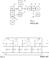
- FIG. 1 shows in a very simplified fashion the main components of an electric vehicle.
- the energy necessary to the traction is stored in a battery pack 45 and may be replenished by the charger 45 or - in the case of a hybrid vehicle - by a non-illustrated combustion motor.
- the battery pack 25 is connected to a power distribution unit 30 that distributes the power to various loads, for instance an DC/DC converter 40 for generating a 12V voltage for auxiliary equipment (entertainment, lights, on-board computers, etc.), and heat pumps 20 for the heating/ear conditioning.
- a high-voltage DC bus 15 transmits the voltage of the battery to a motor drive unit 60 that includes an inverter generating multiphase AC waveforms suitable for the electric traction motor 70.
- An EMI filter 50 is inserted on the DC bus 15 at the supply point of the drive unit 60 to filter out the noise generated by the inverter in the latter.
- figure 1 is just one among the various possibilities and is provided merely as a non-limiting example of one possible use of the invention.
- the invention may be used in electric vehicles presenting various configurations, for example in series-hybrid, parallel-hybrid, plug-in-hybrid configurations that do not correspond to the diagram of figure 1 .
- the invention is not limited to automotive applications, either.
- Figure 1 shows two EMI filters 50, one between battery 25 and charging connector 49, and one on the DC side of the motor drive 60.
- the inventive EMI filter may be used in other positions without leaving the scope of the invention. Meaningful locations for EMI filters are: before and after the charger 45; after the battery 25; before the DC/DC converter 40.
- the charging unit 45 may be totally or in part installed after the connector 49. All these variants are included in the scope of the invention defined by the appended claims.
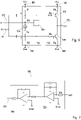
- FIG. 2 shows a possible structure of a passive EMI filter 51 as known in the art.
- the filter is configured as a two-stage LC filter with two common-mode chokes L1 and L2 and several capacitors connected between the positive and negative power rails (X-capacitors C2, C5, C8) or between a power rail and the protective earth conductor (Y-capacitors C1, C3, C4, C6, C7, C9).
- Such filters can be designed to provide an effective attenuation of noise at the price of an increase in size, weight, and manufacturing cost.
- an EMC filter can be designed to attenuate differential and/or common mode noise.
- Common mode noise appears simultaneously with the same polarity on all the conductors of the supply bus and is often dominant.
- the filter of figure 2 is designed to attenuate primarily common-mode noise.
- Figure 3 illustrates a possible structure of a filter 50 according to the invention. It is drawn as a unifilar scheme, and power line 15 is represented by a single line. This is a simplification of a real implementation in which the power line 15 may include several conductors.
- the supply line 15 may be a HVDC bus in an electric vehicle comprising a positive rail and a negative rail.
- the filter may be designed to attenuate a differential noise or, preferably, a common-mode noise component.
- the active filter has a feedback configuration with a current sense unit 110, which could be a current transformer, that reads the noise current flowing out of the output, as an error signal, an analogue signal conditioning stage 120 that is designed to amplify the error signal in a determined frequency band, a current source 130 that inserts, through the current injection circuit 140, a correction current on the supply line 15.
- a current sense unit 110 which could be a current transformer, that reads the noise current flowing out of the output, as an error signal
- an analogue signal conditioning stage 120 that is designed to amplify the error signal in a determined frequency band
- a current source 130 that inserts, through the current injection circuit 140, a correction current on the supply line 15.
- the filter presented has a "current sensing/current injecting" topology that sense a current and inject a corresponding correction current.
- the invention is not limited to this case, however, and may also include filters that sense the noise as a voltage disturbance of the supply line, and/or include a voltage source to inject a voltage on the supply line, or filters with an output circuit that is neither a pure current source nor a pure voltage source.
- the following description will introduce “current sense units” at the input of the filters, and “current sources” at the output but, they could be replaced by voltage sensors, respectively voltage sources, or by sensor and sources that are neither pure current nor pure voltage type, without leaving the scope of the invention.
- Y denotes the signal at the filter's output
- X the signal at the input
- H the open-loop gain.
- additional factors will be introduced by non-ideal behaviour of the sensor, and so on.
- the invention is not limited to this topology of filter and may also include, for example, feed-forward filters.
- Any active filter exhibits a dynamics limit, that is the maximum current that can be injected back on the supply line and rely on a power supply (not represented) for their work. Its performance is guaranteed into a determined bandwidth, where their operating parameters (for example the insertion loss) respect nominal values.
- the bandwidth of the filtering stages will be determined in consideration of the noise bandwidth. In a typical automotive application, a bandwidth of at least 1 MHz is required.
- the active filter is inserted on the supply line after the noise source (eventually with a passive pre-filtering stage) and should be capable of injecting a current having the same intensity as the noise current.
- Demanding applications may have noise amplitudes of 2 A peak-to-peak or more, and the output dynamics of the first active filtering stage should match these figures.
- the required dynamic behaviour can be obtained by a filter configured as shown in figure 4 .
- the current source 130 has a common emitter network 132 whose operating point is determined by a bias network 134 and a PI (proportional-integral) control network 136 for stabilizing the DC component of the output.
- the active filter of the invention has a unipolar supply rather than a more complex bipolar supply with positive and negative voltage rails.
- common emitter network 132 bias network 134
- PI control network 136 PI control network 136
- the three stages: common emitter network 132, bias network 134, and PI control network 136 are designed to work in harmony and behave as a high-frequency voltage-controlled current source.
- the circuit of the invention has proved advantageous because it offers a high output impedance (thus approximating an ideal current source) at high frequency, a good stability, an extended temperature range, and is eminently suitable for building an active EMC filter in automotive applications.
- the current output stage 132 is shown in figure 4 and in the simplified schematic of figure 6 . It has two bipolar transistors in a symmetric common-emitter configuration: a PNP transistor 138 with the emitter connected to the positive supply 185 through a resistor Re of suitable value and a NPN transistors139 with the emitter likewise connected to the negative supply 180, which may be the ground.
- the output 175 of the current stage 132 is at the collectors of the transistors.
- the bases of both transistors are AC-coupled with the HF input signal through the active bias network 134 that will be described further.
- the stage may be configured to operate in class A, with both transistors in the active region always, or in class AB, the PNP transistor being active only for the positive polarity of the output current and the NPN transistor for the negative one, with a small region of class-A operation around the centre point.
- the inventors have found that the common emitter provides a high output impedance, which is desirable, but cannot perform alone satisfactorily in an active EMI filter. Since the output is AC coupled, the load impedance becomes very high at low frequency. Therefore, the DC gain tends to be much higher than the AC gain. This causes a drift of the output DC voltage (preferably at equal distance from the supply rails Vcc and Vee) because the transistors are only imperfectly matched. This instability is particularly dangerous in EMI filters since the current source may end in saturation, injecting deformed waveforms in the system and thus additional noise at high frequency.
- the invention has a control network 136 feeding back the DC value at the output to the correction node 172 (mark 'e') and keeps the output voltage fixed to a reference value.
- the control network 136 may be based on an integrator and a gain stage, implementing a P/I control, as in the simplified schematics of figure 7 , but other configurations are possible.
- the input resistance Rin of the integrator 156 may have a value between 10 k ⁇ and 10 M ⁇ , to avoid loading the output of the stage 132 and to control the time constant of integration.
- the integrator 156 is a low-pass filter and will be designed not to interfere with the high-frequency behaviour of the filter.
- the cut-off frequency of the integrator will be well below the lower cut frequency of the desired EMI filter, for example one decade below.
- the cut-off frequency of the control network should be of 1 kHz maximum.
- the proportional stage 166 increases the accuracy of the control.
- CMOS operational amplifiers exhibit very low input bias currents and exist in single supply rail-to-rail variety. They can be used advantageously in this application.
- the output of the gain stage 166 is an offset DC voltage that is injected in a bias correction node 172 of the bias network 134.
- the active bias network 134 is designed to keep the DC bias of the common emitter network at the desired working point all over the temperature range of interest and to correct the different characteristics of the PNP and NPN transistors. It comprises a voltage reference 164 that keeps a constant voltage across the nodes “d” and “e” in all the temperature range of interest.
- the diode array 154 introduce a negative temperature coefficient, therefore the potential between nodes “c” and “d” changes with the temperature. As the voltage drop on R1 and R2 is kept equal, this leads to a temperature-dependent change in the transistors' base voltages that counterbalances the temperature characteristics of transistors 138 and 139.
- control network 136 feeds back a DC signal 124 directly at a special correction node e of the active bias network k134, and, in so doing, keeps the operating points of the transistors stable in the temperature range of interest.
- This schematics represents a preferred solution but is not the only possibility for the invention.
- the operating point could be controlled also, as shown in figure 5 , by feeding back the DC correction signal through the pre-gain stage 120 rather than directly to the active bias network 134.
- the pre-gain stage 120 produces an input signal 126 for the bias network 134 that combines the HF signal sensed by the current transformer 110 and the DC correction signal 124.
Landscapes
- Engineering & Computer Science (AREA)
- Power Engineering (AREA)
- Physics & Mathematics (AREA)
- Electromagnetism (AREA)
- Computer Networks & Wireless Communication (AREA)
- Signal Processing (AREA)
- Networks Using Active Elements (AREA)
- Filters And Equalizers (AREA)
Priority Applications (4)
| Application Number | Priority Date | Filing Date | Title |
|---|---|---|---|
| EP21157666.5A EP4047802A1 (de) | 2021-02-17 | 2021-02-17 | Emi-aktiver filter |
| US17/670,260 US12081117B2 (en) | 2021-02-17 | 2022-02-11 | High-frequency current source for an active EMI filter, active EMI filter and use of an active EMI filter |
| CN202210141154.7A CN114944752A (zh) | 2021-02-17 | 2022-02-16 | 有源emi滤波器的高频电流源、有源emi滤波器和有源emi滤波器的用途 |
| EP22156959.3A EP4047803B1 (de) | 2021-02-17 | 2022-02-16 | Hochfrequenzstromquelle für einen aktiven emi-filter, aktiver emi-filter und verwendung eines aktiven emi-filters |
Applications Claiming Priority (1)
| Application Number | Priority Date | Filing Date | Title |
|---|---|---|---|
| EP21157666.5A EP4047802A1 (de) | 2021-02-17 | 2021-02-17 | Emi-aktiver filter |
Publications (1)
| Publication Number | Publication Date |
|---|---|
| EP4047802A1 true EP4047802A1 (de) | 2022-08-24 |
Family
ID=74666616
Family Applications (2)
| Application Number | Title | Priority Date | Filing Date |
|---|---|---|---|
| EP21157666.5A Withdrawn EP4047802A1 (de) | 2021-02-17 | 2021-02-17 | Emi-aktiver filter |
| EP22156959.3A Active EP4047803B1 (de) | 2021-02-17 | 2022-02-16 | Hochfrequenzstromquelle für einen aktiven emi-filter, aktiver emi-filter und verwendung eines aktiven emi-filters |
Family Applications After (1)
| Application Number | Title | Priority Date | Filing Date |
|---|---|---|---|
| EP22156959.3A Active EP4047803B1 (de) | 2021-02-17 | 2022-02-16 | Hochfrequenzstromquelle für einen aktiven emi-filter, aktiver emi-filter und verwendung eines aktiven emi-filters |
Country Status (3)
| Country | Link |
|---|---|
| US (1) | US12081117B2 (de) |
| EP (2) | EP4047802A1 (de) |
| CN (1) | CN114944752A (de) |
Families Citing this family (1)
| Publication number | Priority date | Publication date | Assignee | Title |
|---|---|---|---|---|
| CN120454474B (zh) * | 2025-04-23 | 2026-03-27 | 华中科技大学 | 基于相量分析的宽频有源emi滤波器设计方法及系统 |
Citations (4)
| Publication number | Priority date | Publication date | Assignee | Title |
|---|---|---|---|---|
| US6107886A (en) * | 1998-03-31 | 2000-08-22 | Kabushiki Kaisha Toshiba | High-efficiency power amplifier |
| US20030128558A1 (en) * | 2002-01-07 | 2003-07-10 | Toshio Takahashi | Active EMI filter with feed forward cancellation |
| US20040207463A1 (en) * | 2000-03-28 | 2004-10-21 | International Rectifier Corporation | Active filter for reduction of common mode current |
| US20180269781A1 (en) | 2017-03-17 | 2018-09-20 | Schaffner Emv Ag | Active filter |
Family Cites Families (4)
| Publication number | Priority date | Publication date | Assignee | Title |
|---|---|---|---|---|
| US4258243A (en) * | 1979-03-26 | 1981-03-24 | Colt Industries Operating Corp. | Over current protection system for electrical discharge machining apparatus |
| DE60133259D1 (de) * | 2000-12-15 | 2008-04-30 | Halo Lsi Design & Device Tech | Schnelles Programmier- und Programmierverifikationsverfahren |
| US7256643B2 (en) * | 2005-08-04 | 2007-08-14 | Micron Technology, Inc. | Device and method for generating a low-voltage reference |
| US10374510B2 (en) * | 2017-04-07 | 2019-08-06 | Texas Instruments Incorporated | Compensated active electro-magnetic interference filters |
-
2021
- 2021-02-17 EP EP21157666.5A patent/EP4047802A1/de not_active Withdrawn
-
2022
- 2022-02-11 US US17/670,260 patent/US12081117B2/en active Active
- 2022-02-16 EP EP22156959.3A patent/EP4047803B1/de active Active
- 2022-02-16 CN CN202210141154.7A patent/CN114944752A/zh active Pending
Patent Citations (4)
| Publication number | Priority date | Publication date | Assignee | Title |
|---|---|---|---|---|
| US6107886A (en) * | 1998-03-31 | 2000-08-22 | Kabushiki Kaisha Toshiba | High-efficiency power amplifier |
| US20040207463A1 (en) * | 2000-03-28 | 2004-10-21 | International Rectifier Corporation | Active filter for reduction of common mode current |
| US20030128558A1 (en) * | 2002-01-07 | 2003-07-10 | Toshio Takahashi | Active EMI filter with feed forward cancellation |
| US20180269781A1 (en) | 2017-03-17 | 2018-09-20 | Schaffner Emv Ag | Active filter |
Also Published As
| Publication number | Publication date |
|---|---|
| EP4047803A1 (de) | 2022-08-24 |
| US12081117B2 (en) | 2024-09-03 |
| CN114944752A (zh) | 2022-08-26 |
| EP4047803B1 (de) | 2025-09-24 |
| US20220263407A1 (en) | 2022-08-18 |
Similar Documents
| Publication | Publication Date | Title |
|---|---|---|
| KR100614267B1 (ko) | 능동 emi 필터 | |
| US7595687B2 (en) | Apparatus and method for reducing EMI generated by a power conversion device | |
| KR102580800B1 (ko) | 능동형 전류 보상 장치 | |
| US4523152A (en) | High-efficiency feedforward-error-correction amplifier | |
| KR102950167B1 (ko) | 전자기 간섭 필터 | |
| EP4047803B1 (de) | Hochfrequenzstromquelle für einen aktiven emi-filter, aktiver emi-filter und verwendung eines aktiven emi-filters | |
| US9407219B2 (en) | Electronic Circuit | |
| US10931242B2 (en) | Error amplifier | |
| US11855600B2 (en) | High frequency, high output impedance amplifier for EMI active filter applications | |
| CN112234951A (zh) | 共模有源emi滤波器 | |
| JP7534599B2 (ja) | 直流電源装置および電源ラインのノイズ抑制方法 | |
| US12341483B2 (en) | Multistage active filter for automotive applications | |
| KR102129578B1 (ko) | 전류 보상 장치 | |
| CN112165311A (zh) | 接入电力电子变换器系统接地回路的有源emi滤波器及系统 | |
| KR20250047683A (ko) | 단일 칩 집적회로를 포함하는 능동형 전류 보상 장치 | |
| CN113328617B (zh) | 一种有源共模电磁干扰滤波器、电源管理装置及滤波方法 | |
| WO2013119640A1 (en) | Low power microphone circuits for vehicles | |
| KR102208533B1 (ko) | 능동형 전류 보상 장치 | |
| KR102857923B1 (ko) | 집적회로부와 비집적회로부를 포함하는 능동형 전류 보상 장치 | |
| JP7506699B2 (ja) | インピーダンスの大きさを制御する電磁干渉フィルター | |
| CN113381714B (zh) | 一种采用交流通路前馈拓扑结构的反相运算放大器 | |
| KR20230136095A (ko) | 능동형 전류 보상 장치 | |
| CN120090504A (zh) | 电机驱动电路、车载设备及车辆 | |
| CN121688731A (zh) | 车辆、旋变励磁保护电路及具有其的电机驱动系统 |
Legal Events
| Date | Code | Title | Description |
|---|---|---|---|
| PUAI | Public reference made under article 153(3) epc to a published international application that has entered the european phase |
Free format text: ORIGINAL CODE: 0009012 |
|
| STAA | Information on the status of an ep patent application or granted ep patent |
Free format text: STATUS: THE APPLICATION HAS BEEN PUBLISHED |
|
| AK | Designated contracting states |
Kind code of ref document: A1 Designated state(s): AL AT BE BG CH CY CZ DE DK EE ES FI FR GB GR HR HU IE IS IT LI LT LU LV MC MK MT NL NO PL PT RO RS SE SI SK SM TR |
|
| STAA | Information on the status of an ep patent application or granted ep patent |
Free format text: STATUS: THE APPLICATION IS DEEMED TO BE WITHDRAWN |
|
| 18D | Application deemed to be withdrawn |
Effective date: 20230225 |