EP4049852A1 - Élément de sécurité, support de données et procédé de fabrication - Google Patents
Élément de sécurité, support de données et procédé de fabrication Download PDFInfo
- Publication number
- EP4049852A1 EP4049852A1 EP22020067.9A EP22020067A EP4049852A1 EP 4049852 A1 EP4049852 A1 EP 4049852A1 EP 22020067 A EP22020067 A EP 22020067A EP 4049852 A1 EP4049852 A1 EP 4049852A1
- Authority
- EP
- European Patent Office
- Prior art keywords
- color
- visible
- security element
- area
- colors
- Prior art date
- Legal status (The legal status is an assumption and is not a legal conclusion. Google has not performed a legal analysis and makes no representation as to the accuracy of the status listed.)
- Granted
Links
Images


Classifications
-
- B—PERFORMING OPERATIONS; TRANSPORTING
- B42—BOOKBINDING; ALBUMS; FILES; SPECIAL PRINTED MATTER
- B42D—BOOKS; BOOK COVERS; LOOSE LEAVES; PRINTED MATTER CHARACTERISED BY IDENTIFICATION OR SECURITY FEATURES; PRINTED MATTER OF SPECIAL FORMAT OR STYLE NOT OTHERWISE PROVIDED FOR; DEVICES FOR USE THEREWITH AND NOT OTHERWISE PROVIDED FOR; MOVABLE-STRIP WRITING OR READING APPARATUS
- B42D25/00—Information-bearing cards or sheet-like structures characterised by identification or security features; Manufacture thereof
- B42D25/20—Information-bearing cards or sheet-like structures characterised by identification or security features; Manufacture thereof characterised by a particular use or purpose
- B42D25/29—Securities; Bank notes
-
- B—PERFORMING OPERATIONS; TRANSPORTING
- B42—BOOKBINDING; ALBUMS; FILES; SPECIAL PRINTED MATTER
- B42D—BOOKS; BOOK COVERS; LOOSE LEAVES; PRINTED MATTER CHARACTERISED BY IDENTIFICATION OR SECURITY FEATURES; PRINTED MATTER OF SPECIAL FORMAT OR STYLE NOT OTHERWISE PROVIDED FOR; DEVICES FOR USE THEREWITH AND NOT OTHERWISE PROVIDED FOR; MOVABLE-STRIP WRITING OR READING APPARATUS
- B42D25/00—Information-bearing cards or sheet-like structures characterised by identification or security features; Manufacture thereof
- B42D25/30—Identification or security features, e.g. for preventing forgery
- B42D25/36—Identification or security features, e.g. for preventing forgery comprising special materials
- B42D25/378—Special inks
- B42D25/382—Special inks absorbing or reflecting infrared light
-
- B—PERFORMING OPERATIONS; TRANSPORTING
- B42—BOOKBINDING; ALBUMS; FILES; SPECIAL PRINTED MATTER
- B42D—BOOKS; BOOK COVERS; LOOSE LEAVES; PRINTED MATTER CHARACTERISED BY IDENTIFICATION OR SECURITY FEATURES; PRINTED MATTER OF SPECIAL FORMAT OR STYLE NOT OTHERWISE PROVIDED FOR; DEVICES FOR USE THEREWITH AND NOT OTHERWISE PROVIDED FOR; MOVABLE-STRIP WRITING OR READING APPARATUS
- B42D25/00—Information-bearing cards or sheet-like structures characterised by identification or security features; Manufacture thereof
- B42D25/30—Identification or security features, e.g. for preventing forgery
- B42D25/36—Identification or security features, e.g. for preventing forgery comprising special materials
- B42D25/378—Special inks
- B42D25/387—Special inks absorbing or reflecting ultraviolet light
Definitions
- the invention relates to a security element for protecting valuables, a data carrier with such a security element, and a method for producing such a security element.
- Data carriers such as value or ID documents, but also other valuables, such as branded items, are often provided with security elements for protection, which allow the authenticity of the data carrier to be checked and which at the same time serve as protection against unauthorized reproduction.
- security elements for protection, which allow the authenticity of the data carrier to be checked and which at the same time serve as protection against unauthorized reproduction.
- luminescent substances it is known to use luminescent substances to protect valuable or identity documents. The presence of the luminescent substances can then be checked, for example, with the aid of a UV lamp.
- inkjet printers have become readily available, with which potential counterfeiters can produce impression counterfeits of banknotes which, at first glance, bear a close resemblance to the original.
- the printing can be done without observation by third parties and without the possibility of tracing back to a specific person.
- inkjet fluorescent colors are also relatively easily available, especially through online trading, so that luminescence characteristics can also be simulated with the help of inkjet printers.
- the invention is based on the object of specifying security elements and documents of value which, in addition to an attractive appearance, have a high level of protection against forgery and are protected in particular against replication using office printers such as multicolor inkjet printers.
- a generic security element has a feature area that contains a first color area that is formed from visually visible printing inks.
- the security element also contains a second color area, which is formed from luminescent substances that are not visible without excitation and which at least partially overlaps the feature area.
- the first color area of the feature area When viewed with the naked eye in visible light, the first color area of the feature area shows a homogeneous appearance with a visible color that is uniform at least in areas. As explained in more detail below, the shape of the first color area can show a visually visible motif within a different-colored environment. When viewed under UV or IR excitation light, the feature region exhibits at least two different luminescent colors.
- the first color area contains a microstructure arrangement of differently colored microstructure elements, which have a characteristic dimension below the resolution limit of the human eye and which each have one of at least two different colors and, through color mixing, produce the uniform color that is visible to the naked eye at least in regions.
- luminescence includes phosphorescence and fluorescence, with the excitation of luminescence with non-visible UV radiation or IR radiation can take place.
- the luminescent substances are preferably transparent in the visible spectral range.
- a homogeneous appearance when viewed with the naked eye means in particular that the viewer cannot see any structures from a normal viewing distance of 25 cm or more, but that the first color area creates the impression of an evenly printed area.
- the color of the first color area of the feature area is in each case uniform at least in areas; the first color area preferably even shows only a single uniform visible color.
- At least two luminescent substances of the second color range which produce two different luminescent colors, lie entirely within a region of the first color range with a uniform visible color.
- the luminescence colors of the feature area generated by excitation preferably differ from the respective uniform visible colors of the feature area, in particular they differ from this in the case of a single uniform visible color.
- the second color area advantageously has two or more luminescence areas which are designed in the form of patterns, characters or codes and which each show one of the different luminescence colors under UV or IR excitation light.
- the second color area can be located entirely within the feature area and only cover part of the feature area. However, it is also possible for the second color area to completely cover the feature area and/or for the second color area also to be partially outside of the feature area. In According to an advantageous embodiment, the second color range lies completely within the first color range.
- the microstructure elements have two or more different colors which, from the normal viewing distance, produce the color impression to be perceived by the viewer through color mixing, in particular subtractive color mixing.
- a background color for example the color of the carrier to which the microstructure elements are applied, can also contribute to the mixed color.
- this background color is often white, but it can also be provided by a colored underprint layer.
- the background color can be present in particular in interstices between the microstructure elements and/or in gaps in the microstructure elements and can contribute to the mixed color.
- the different colors of the microstructure elements in the CIELab system have a color difference ⁇ E of at least 4.0, preferably at least 6.0.
- the microstructure elements of the first color area can be arranged next to one another or also at a distance from one another.
- the microstructure elements can be represented positively in the form of geometric symbols, Letters and/or numbers and/or in negative representation as a surface with recesses in the form of geometric symbols, letters and/or numbers. In particular, line fragments, squares, triangles or other polygons, each with or without filling, come into consideration as geometric symbols.
- the microstructure elements advantageously at least partially accommodate geometric elements that can be seen with the naked eye elsewhere in the security element, in order to create a connection between the various elements of the security element. Such a relationship also facilitates recognition or identification of the content of information encoded by the microstructure.
- the characteristic dimension of the microstructure elements is given, for example, by the diameter of the geometric symbols or the line thickness of letters or numbers. In the case of negative representations, the distance between adjacent recesses forms a characteristic dimension of the microstructure elements. Irrespective of the specific design of the microstructure arrangement, it is only essential that the microstructure elements are not recognizable as such with the naked eye due to their small dimensions from a normal viewing distance of 25 cm or more, but that the microstructure arrangement is characterized by the color mixture of the element colors as in a fine print grid is perceived as a homogeneous surface.
- the microstructure elements contain a first group of microstructure elements in a first color in negative representation and a second group of microstructure elements in a second, different color in positive representation, the microstructure elements of the second group are arranged in the recesses of the first group of microstructure elements.
- the luminescent substances of the second color range are admixed at least in some areas to the visually visible printing inks of the first color range and thereby form printing inks that are both visually visible and luminescent.
- the luminescent substances of the second color range can be present at least in regions in a luminescent layer arranged above and/or below the visually visible printing inks.
- the luminescent substances of the second color range are present in a luminescence layer arranged below the visually visible printing inks and the visually visible printing inks of the first color range contain a UV blocker in certain areas, which causes UV excitation at least in a partial range of the UV spectrum between 200 nm and 400 nm reduced or prevented.
- a further development of the invention provides that the first and second color areas are overprinted with a line structure with a non-luminescent, visually visible color whose color differs from the uniform color or colors of the first color area.
- the line structure preferably takes up geometric shapes recognizable with the naked eye elsewhere in the security element, in particular the outline shape of a luminescent or non-luminescent partial area of the feature area. With the additional line structure any visible color differences, gloss differences and/or register fluctuations of the visually visible printing colors are masked.
- the at least two different macroscopic luminescence regions have a luminescent outer contour of a different color, the hue of which corresponds to the respective other luminescence color or a mixed color of the two luminescence colors.
- the microstructure arrangement is advantageously arranged on a transparent or opaque carrier, in particular on a transfer film element.
- the microstructure arrangement can in particular be arranged directly on the carrier, in particular printed onto the carrier.
- the security element is advantageously a security thread, in particular a window security thread or a pendulum security thread, a tear-open thread, a security band, a security strip, a patch or a label for application to security paper, a document of value or the like.
- the security element can contain a carrier film or be present without a carrier film.
- the microstructure arrangement and/or the luminescent substances are advantageously applied in offset printing, relief printing, indirect relief printing, gravure printing or in a digital printing process such as ink-jet printing or laser printing processes.
- the second color range preferably even shows only a single uniform luminescent color.
- the uniform luminescence colors of the feature area generated upon excitation, or the single uniform luminescence color advantageously differ from the colors of the feature area that are visible in visible light.
- the first color area advantageously has two or more color areas which are designed in the form of patterns, characters or a code and which each show one of the different visible colors in visible light.
- the microstructure elements have two or more different luminescence colors that produce the color impression to be perceived by the viewer from the normal viewing distance through color mixing, in particular additive color mixing and absorption of the emission color by the visually visible colors.
- a luminescent background color can also contribute to the mixed color. It is advantageously provided that the different luminescence colors of the microstructure elements in the CIELab system have a color difference ⁇ E of at least 4.0, preferably at least 6.0.
- the microstructure elements of the second color area can be arranged adjacent to one another or also at a distance next to one another.
- the microstructure elements can be in the form of geometric symbols, letters and/or numbers in a positive representation and/or in a negative representation as a surface with gaps in the form of geometric symbols, letters and/or numbers.
- line fragments, squares, triangles or other polygons, each with or without filling come into consideration as geometric symbols.
- the microstructure elements advantageously at least partially accommodate geometric elements that can be seen with the naked eye elsewhere in the security element, in order to create a connection between the various elements of the security element. Such a relationship also facilitates recognition or identification of the content of information encoded by the microstructure.
- the characteristic dimension of the microstructure elements is given, for example, by the diameter of the geometric symbols or the line thickness of letters or numbers. In the case of negative representations, the distance between adjacent recesses forms a characteristic dimension of the microstructure elements. Regardless of the specific design of the microstructure arrangement, it is only essential that the microstructure elements are not recognizable with the naked eye due to their small dimensions from the normal viewing distance of 25 cm or more, but that the microstructure arrangement is due to the additive color mixture of the luminescent colors of the elements as is perceived as a homogeneous surface with a fine print screen.
- the microstructure elements contain a first group of microstructure elements of a first luminescence color in negative representation and a second group of microstructure elements of a second, different luminescence color in positive representation, the microstructure elements of the second group being arranged in the recesses of the first group of microstructure elements.
- the luminescent substances of the second color range are admixed at least in some areas to the visually visible printing inks of the first color range and thereby form printing inks that are both visually visible and luminescent.
- the luminescent substances of the second color range can be present at least in regions in a luminescent layer arranged above and/or below the visually visible printing inks.
- the invention also includes a data carrier with a security element of the type described.
- the data carrier can in particular be a document of value, such as a banknote, in particular a paper banknote, a polymer banknote or a foil composite banknote, a share, a bond, a certificate, a voucher , a cheque, a seal, a tax stamp, a high-value admission ticket, but also an identification card, such as a credit card, a bank card, a cash payment card, an authorization card, an ID card or a passport personalization page.
- a banknote in particular a paper banknote, a polymer banknote or a foil composite banknote, a share, a bond, a certificate, a voucher , a cheque, a seal, a tax stamp, a high-value admission ticket
- an identification card such as a credit card, a bank card, a cash payment card, an authorization card, an ID card or a passport personalization page.
- the security element can be a separate security element, for example a film element that is attached at a desired location on a Disk is arranged.
- the security element can also form an integral part of the data carrier itself, for example by an imprint which is applied to a substrate of the data carrier.
- figure 1 shows a schematic representation of a bank note 10, which has a substrate made of paper, plastic or a hybrid substrate a combination of paper and plastic layers.
- the banknote 10 is provided with three security elements 12, 16 and 18 according to exemplary embodiments of the invention, the first security element being a security thread 12 which emerges at certain window areas 14 on the surface of the banknote 10, while in the areas lying in between it is inside the Banknote 10 is embedded.
- the second security element 16 is formed by a partial area of the banknote 10 in which the banknote paper is provided with an imprint which has the various special color areas described in more detail below.
- the third security element 18 is formed by a partial area of the banknote 10 in which the banknote paper is provided with a motif-shaped imprint, namely an imprint with a recess in the form of the denomination “10” of the banknote. This print also has the special color areas described below.
- the invention does not extend to 1 security elements shown as an example is limited, but in particular also includes glued-on transfer elements of any shape with or without their own carrier film.
- the security element can also be designed in the form of a cover film, which is arranged over a window area or a continuous opening of the bank note.
- the invention can be used for all types of security elements, for example also for labels on goods and packaging or for protecting documents, identity cards, passports, credit cards, health cards and the like.
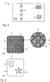
- figure 2 shows a plan view of a security element 20 according to a first embodiment of the invention, wherein Fig.2(a) the appearance of the security element in visible light and Fig.2(b) represents the appearance of the security element under UV light.
- the security element 20 When viewed in visible light, the security element 20 appears to the naked eye from a normal viewing distance of approximately 30 cm as a homogeneous surface 22 with a uniform color, for example red Fig.2(a) illustrated, the surface that appears monochrome is actually formed from a large number of small microstructure elements 24, 26, all of which have a dimension below the resolution limit of the human eye and are therefore themselves not visible to the naked eye.
- the microstructure elements are formed by squares 24, 26 measuring 80 ⁇ m ⁇ 80 ⁇ m, each of which has a recess 28 in the form of letters or numbers, as in FIG Fig.2(a) illustrated by the letters "A" and "B" respectively.
- the squares 24 are printed directly onto the banknote paper of a banknote 10 using a printing ink with yellow color pigments, and the squares 26 using a printing ink with magenta-colored color pigments.
- the differently colored squares 24, 26 produce the mixed color red of the surface 22 by subtractive color mixing, the color saturation of the red color impression being able to be adjusted by the size of the gaps 28.
- figure 2 shows the same size Squares 24, 26, but the microstructures can also have different sizes, for example to produce a mixed color of a desired hue.
- the surface 22, which appears homogeneously monochrome from a normal viewing distance, actually consists of the differently colored squares 24, 26 with their letter-shaped recesses 28 can be determined with a magnifying glass or a microscope and represents an authenticity feature of the security element 20 that is difficult to reproduce.
- the security element 20 When viewed under UV light, the security element 20 shows the in Fig.2(b) shown appearance with two lying within the area 22, motif-shaped luminescence areas 30, 32, which shine with different luminescence colors, such as orange and green. Both luminescence colors are different from the visible red color of the surface 22, so that the luminescence areas 30, 32 appear in clearly contrasting fashion even with the combination of visible and UV light that is usually present.
- the luminescence areas 30, 32 are not recognizable, the same homogeneous, red appearance is visible in their surface areas as in the rest of the surface 22, so that the position of the luminescence areas in Fig.2(a) is only indicated by dashed lines.
- the homogeneously appearing surface 22 forms the abovementioned first color area and at the same time the feature area congruent to the first color area, and the luminescence areas 30, 32 together form the abovementioned second color area which overlaps the feature area.
- the second color area located entirely within the feature area.
- the microscopic microstructure elements 24, 26 and the macroscopic luminescence areas 30, 32 can advantageously be matched to one another.
- the recesses 28 of the microstructure elements 24, 26 can be formed alternately in the form of the digits "1" and "0" of the denomination "10" of the bank note, and the two luminescence areas 30, 32 can also be in the form of the digits "1" and "0” may be applied to represent the value number under UV illumination.
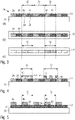
- FIG 3 shows in (a) schematically the structure of a security element 20 according to an embodiment of the invention in cross section, the Figures 3(b) and 3(c) illustrate the associated appearance of the security element when viewed in visible light or in UV light in plan view.
- the security element 20 has a substrate 36, which in particular represents the substrate of the document of value on which the security element 20 is applied, for example printed.
- the substrate 36 it is also possible for the substrate 36 to be a substrate film of a separate security element which, after it has been produced, is applied, for example glued, to a desired target substrate.
- the security element 20 can also be produced on a transfer carrier substrate, transferred to the target substrate and the transfer carrier substrate then pulled off.
- the surface 22 is formed by a sequence of microstructure elements 24, 26, which are formed, for example, by printing inks with yellow or magenta color pigments.
- the microstructure elements can also contain recesses, as in 2 shown, but for the sake of simplicity in 3 are not shown.
- the microstructure elements can be applied adjacent to one another or next to one another at a small distance. Due to the small dimensions of the microstructure elements 24, 26, the surface 22 appears from a normal viewing distance with the uniform subtractive mixed color of the yellow and magenta microstructure elements, ie in a uniform red color.
- the printing inks of the microstructure elements 24, 26 in the first luminescence regions 30 are admixed with a first luminescent substance 40 which is transparent in the visible spectral range and therefore does not affect the visual colors of the microstructure elements.
- a second luminescent substance 42 that is transparent in the visible range is added to the printing inks of the microstructure elements 24, 26.
- the luminescent colors of the first and second luminescent substances 40, 42 differ from one another and also differ from the mixed color of the surface 22.
- the non-luminescent regions 34 the printing inks of the microstructure elements 24, 26 are present without the admixture of luminescent substances.
- the luminescent areas 30, 32 are formed macroscopically in the form of characters or patterns, such as the coat of arms motif or the star motif Fig.2(b) .
- the luminescence areas have such large dimensions that, in contrast to the microstructure elements 24, 26, they can be seen with the naked eye from a normal viewing distance, ie they each contain a large number of microstructure elements 24, 26.
- the Luminescence regions 30, 32 can be continuous or rastered, ie formed by small luminescent raster elements that cannot be resolved with the naked eye, which together form the desired luminescence motif from a normal viewing distance.
- Six different printing inks are therefore used to print surface 22, namely the visually visible printing ink with the first color (yellow) without the addition of luminescent substance, the visually visible printing ink of the first color with the addition of the first luminescent substance 40 or the second luminescent substance 42 , the visually visible printing ink of the second color (magenta) without admixture of luminescent substance and the visually visible printing ink of the second color with admixture of the first luminescent substance 40 or the second luminescent substance 42.
- the transparent luminescent substances do not appear when viewed in the visible spectral range.
- the sequence of the differently colored microstructure elements 24, 26 can be seen with a magnifying glass; with the naked eye, the color effects of the microstructure elements 24, 26 mix to form the uniform mixed color of the surface 22.
- the luminescent areas 30, 32 glow in the corresponding luminescent colors, as shown in FIG 3(c) illustrated.
- the colors of the microstructure elements 24, 26 appear in addition to the luminescence colors, so that the luminescence regions 30, 32 appear against the background of the mixed color of the surface 22 with the naked eye.
- figure 4 shows a modification of the design of the 3 , in which the luminescent substances 40, 42 are not mixed with the printing inks of the microstructure elements 24, 26, but are printed separately as visually transparent, luminescent printing inks 50, 52 on the printing layer with the microstructure elements 24, 26.
- a registration of the macroscopic luminescence regions 30, 32 to the microstructure elements 24, 26 is not absolutely essential in this embodiment.
- the luminescence areas can be both continuous (illustrated in the luminescence area 30) or rastered (illustrated in the luminescence area 32), i.e. formed by small luminescent raster elements 38 that cannot be resolved with the naked eye, which form the desired luminescence motif from the normal viewing distance in the manner of a raster image generate.
- the printing inks 50, 52 can be printed onto the microstructure elements 24, 26, as in 4 illustrated, or below the microstructure elements 24, 26 are present. In the latter case, the light emitted after UV excitation passes through the printing inks of the microstructure elements 24, 26, so that the perceptible luminescence colors result from the emitted luminescence colors and the absorption properties of the printing inks of the microstructure elements. It goes without saying that the luminescent printing inks 50, 52 can also be present partially above and partially below the microstructure elements 24, 26. The technological challenge of this design consists in particular in the registration of the microstructure elements 24, 26 in order to produce the homogeneously single-colored surface 22.
- the visually invisible luminescent printing ink is printed more or less well registered in the area of the first visually visible microstructure color, for example yellow, and for the second luminescent area in the area of the second visually visible microstructure, for example magenta.
- a white luminescence color is used, a yellow and a magenta luminescence image appears due to the interaction with the background color figure 5 shows a further modification of the design of the 3
- the printing ink for the microstructure elements 24' is formulated to be opaque and these microstructure elements 24' are printed onto previously applied microstructure elements 26'.
- the opaque printing ink of the microstructures 24' partially covers the microstructures 26' arranged underneath, so that essentially only the opaque printing ink appears at the overprinted areas. Since the printing ink provided with a luminescent substance 40 or 42 also has an opaque effect, only the luminescent substance of the opaque printing ink is excited to emit in the luminescent areas 30 or 32 in the overprinted areas. Accordingly, the result is essentially an appearance as in 3(b) in visible light and an appearance as in 3(c) in UV light.
- figure 6 shows yet another modification of the design of the 3 , in which a continuous luminescent layer 60 is present on the substrate 36, occupying the entire area 22 and containing a first luminescent substance 40 in partial areas and a second luminescent substance 42 in partial areas.
- the microstructure elements 24, 26 are printed onto the luminescence layer 60, with the printing inks of the microstructure elements 24, 26 in the non-luminescence areas 34 being admixed with a UV blocker 62 which prevents UV excitation of the luminescence substances 40, 42 at these points.
- the luminescence substances 40, 42 can be excited through the visible printing inks and the luminescence emission, each filtered through the printing inks of the microstructure elements 24, 26, can be observed.
- the overall appearance is essentially as in 3(b) in visible light and an appearance as in 3(c) in UV light. There is no filtering of the emission color in areas of the luminescence layer 60 without overprint by visually visible printing inks or in gaps in the visually visible printing inks.
- IR-excitable luminescent substances are used, corresponding NIR absorbers must be used instead of the UV blockers in order to achieve the desired prevention of IR excitation.
- FIG. 7 shows in (a) schematically the structure of a security element 20 in cross section and in (b) and (c) the associated appearance when viewed in visible light or in UV light in plan view.
- surface 22 is referenced to FIG Fig.7(a) formed by a succession of microstructure elements 24, 26, which are applied with small gaps 70 on the substrate 36.
- the dimensions of the gaps 70 are of the same order of magnitude as the dimensions of the microstructure elements 24, 26.
- the gaps 70 are filled with visually transparent, luminescent printing inks 50, 52, which are filled with first and second luminescent substances 40, 42 are provided.
- the luminescent printing inks 50, 52 arranged there represent small printing dots or printing elements of a raster image and form the desired motifs of the luminescent areas from a normal viewing distance, without the raster itself being able to be resolved with the naked eye.
- the transparent, luminescent printing inks 50, 52 do not appear when viewed in the visible spectral range.
- the sequence of the differently colored microstructure elements 24, 26 spaced apart from one another can be seen with a magnifying glass; when viewed with the naked eye at a normal viewing distance, their color effects mix to form the uniform mixed color of the surface 22.
- the luminescent areas 30, 32 When viewed under UV light, the luminescent areas 30, 32 light up in the corresponding luminescent colors, as shown in FIG Fig.7(c) illustrated, wherein the luminescent spaces as described produce the desired luminescent motifs in the manner of raster images.
- the luminescent substances can differ from one another in particular in the excitation spectrum, in the emission spectrum and in the afterglow duration.
- FIG. 12 illustrates some advantageous configurations for dividing the visually homogeneous appearing surface into microstructure elements in the form of different signs and symbols.
- An enlarged section of the surface of the first color area with the microstructure elements is shown schematically in each case. With the naked eye, the surface appears homogeneous from a normal viewing distance, as already explained above.
- microstructure elements 82 of a first color contains the homogeneously appearing surface 80 microstructure elements 82 of a first color, and microstructure elements 84 of a second, different color.
- the microstructure elements are each formed by letters of a specific font in the same font size and are printed on a white substrate base 86 .
- the line width of the letters is, for example, 10 ⁇ m to 30 ⁇ m and the letter height is 30 ⁇ m to 100 ⁇ m.
- the letters of the differently colored microstructure elements 82, 84 form the word “TALER” as a hidden code that is only visible with a magnifying glass.
- the color of the initials "T” changes constantly in order to create a color impression of the surface 80 that is as uniform as possible from the normal viewing distance.
- the hue of the surface 80 results from the two different colors of the microstructure elements 82, 84 and the white color of the substrate background 86.
- the color of the first letters of each line also advantageously changes from line to line in order to avoid monochrome border lines.
- Fig.8(b) shows a modification of the design of the 8(a) , in which the legibility of the microwriting formed by the microstructure elements is increased by the addition of a star-shaped separation symbol 88.
- the separator symbol 88 preferably has substantially the same area coverage as the letter symbols so as not to introduce perceptible clutter in the character string.
- the addition of the separation symbol 88 results in the further advantage that the color of the initial letter "T" can now always be the same, thereby increasing the legibility of the coded word under a magnifying glass. It is understood that instead of the in Fig.8(b) Sterns also used others symbols, and that multiple separator symbols can also be used.
- Figures 8(a) and (b) Use positive representations of the characters is in the design of the Fig.8(c) a negative representation of the letters is used for the area 80, with which a higher color coverage is achieved.
- the surface 80 as well as in the design of 2 , formed by a sequence of square microstructure elements 92, 94 in two different colors, the squares each containing a centered recess 98 in the form of the letters of the encoded word "TALER".
- the mixed color of the surface 80 results from the colors of the microstructure elements 92, 94 and the white color of the substrate background in the recesses 98.
- the homogeneously appearing surface 80 is formed on the one hand by a negative microstructure 102 of a first color and on the other hand by a positive microstructure 104 of a second color.
- the negative microstructure 102 contains recesses in the form of the letters of the word "TALER”, while the positive microstructure 104 contains the same letters in positive representation, which are arranged in the recesses of the negative microstructure 102 in each case.
- the unprinted portion of the substrate is further reduced by such a combination of two positive/negative microstructures and a high color strength is achieved.
- the first color area 110 of a security element can also contain a plurality of partial areas 112, 114, in which the area 80 which appears homogeneous appears in each case with a different mixed color.
- a negative microstructure 102 of a first color and a positive microstructure 104 of a second color are present in a first partial area 112, and a negative microstructure 106 of a third color combined with the positive microstructure 104 of the second color ( or a fourth color).
- surface 80 From a normal viewing distance, surface 80 then appears homogeneous and with a uniform color in both sub-area 112 and sub-area 114, with the uniform color in first sub-area 114 resulting from subtractive color mixing of the first and second colors, and the uniform color in the second sub-area 116 by subtractive color mixing of the third and second color (or the third and fourth color).
- the color of the positive microstructure 104 can also change from the first to the second partial area.
- the partial areas of different colors can be spaced apart or directly adjacent to one another. More than two partial areas with different mixed colors can also be provided.
- the mixed colors of these several partial areas are matched to one another in such a way that, from the normal viewing distance, they appear as a quasi-continuous color progression between two areas with fixed but different mixed colors.
- figure 9 shows a further development of the security element 20 of FIG figures 2 and 3 , in which the first color area 22 and the second color area 30, 32 are overprinted with a line structure 120, the hue of which differs from the uniform red mixed color of the first color area.
- the structure 120 can also be produced by leaving out the visually visible colors.
- the line structure 120 can be configured as desired but preferably adopts a geometric shape present in the partial regions 30, 32 or 34, in the exemplary embodiment approximately the star shape of the second luminescence region 32.
- the additional line structure 120 masks any perceptible color differences, gloss differences and/or register fluctuations between the partial areas 30, 32 or 34, which in some cases can remain despite the basic color equality and the visual transparency of the luminescent substances.
- the line structure 120 is printed with a visually visible, non-luminescent ink so that it has the masking effect described when viewed in visible light, as in FIG 9(a) illustrated.
- the line structure 120 appears darker in the luminescence areas 30, 32 since it reduces the emission of the luminescent substances there.
- Fig.9(b) This effect is shown for clarification with an exaggerated line thickness of the line structure 120 in the case of a complete blocking of the luminescence emission.
- Figures 10 and 11 illustrate another design of a security element 200, wherein 10(a) the appearance of the security element 200 in visible light and 10(b) represents the appearance of the security element under UV light.
- figure 11 shows schematically the structure of the security element 200 in cross section along the line XI-XI of FIG 10(a) .
- the security element 200 appears in visible light with two or more different colors in an area 202, with 10(a) two color areas 204, 206 of different colors are shown for illustration, which are separated by an unprinted intermediate area 208.
- the appearance of the security element 200 changes, so that when viewed with the naked eye from a normal viewing distance of about 30 cm, both color areas 204, 206 now glow in the same luminescent color as in FIG 10(b) illustrated.
- the two motifs 204 (coat of arms and star) can appear red against a blue background 206 in visible light, while under UV light both the two motifs 204 and the background 206 appear with yellow luminescence.
- the monochromatic luminescent surface is actually composed of a multiplicity of small luminescent microstructure elements 224, 226 which have a dimension below the resolution limit of the human eye and are therefore not visible to the naked eye itself.
- the monochromatic luminescent surface 202 is formed by a negative microstructure 224 with a first luminescent color, for example red, and a positive microstructure 226 with a second luminescent color, for example green, which together produce the yellow luminescent color of the surface 202 through additive color mixing.
- the negative microstructure 224 contains the letters of the encoded word "TALER" as recesses, while the positive microstructure 226, congruent with the recesses of the negative microstructure 224, contains the same letters in positive representation.
- the security element 200 has a substrate 36 which, as in the configurations described above, can be, for example, a substrate film of the security element itself or the substrate of a document of value to which the security element is applied.
- the two differently colored color areas 204, 206 are printed onto the substrate 36 with visually visible printing inks.
- a luminescence layer 220 which is formed by the above-mentioned sequence of elements of the negative microstructure 224 and the positive microstructure 226, is applied to both color areas.
- the negative microstructure 224 contains a first luminescent substance 214 which luminesces red after UV excitation and the positive microstructure 226 contains a second luminescent substance 216 which luminesces green after UV excitation. Due to the small dimensions of the microstructure elements 224, 226, the area 202 appears from a normal viewing distance in UV light with the uniform additive mixed color yellow.
- the composite character of the surface 202 can be verified as an authenticity feature using a magnifying glass or a microscope.
- microstructure elements 224, 226 can also be applied in other arrangements, in particular in one of the above with reference to FIG Figures 8(a) to 8(e) described arrangements.
- the luminescent substances 214, 216 can also each be mixed with a visually visible printing ink, as shown in FIG 12 illustrated.
- the luminescent substances 214 and 216 in the color areas 206 are each mixed with a blue printing ink, and the two printing inks 234, 236 thus obtained are printed alternately in the form of the microstructure elements 224, 226 in order to produce the background area 206.
- the luminescent substances 214 and 216 are each mixed with a red printing ink, and the two printing inks 244, 246 thus obtained are printed alternately in the form of the microstructure elements 224, 226 in order to produce the red motif areas 204.
- the above-described appearance of the security element 200 also results in this variant.
- the exemplary embodiments were each described with reference to UV light as the excitation radiation, but it goes without saying that luminescent substances which can be excited to luminescence by IR light can also be used in the same way.
Landscapes
- Business, Economics & Management (AREA)
- Accounting & Taxation (AREA)
- Finance (AREA)
- Printing Methods (AREA)
- Credit Cards Or The Like (AREA)
Applications Claiming Priority (1)
| Application Number | Priority Date | Filing Date | Title |
|---|---|---|---|
| DE102021001019.1A DE102021001019A1 (de) | 2021-02-25 | 2021-02-25 | Sicherheitselement, Datenträger und Herstellungsverfahren |
Publications (2)
| Publication Number | Publication Date |
|---|---|
| EP4049852A1 true EP4049852A1 (fr) | 2022-08-31 |
| EP4049852B1 EP4049852B1 (fr) | 2024-01-31 |
Family
ID=81326226
Family Applications (1)
| Application Number | Title | Priority Date | Filing Date |
|---|---|---|---|
| EP22020067.9A Active EP4049852B1 (fr) | 2021-02-25 | 2022-02-18 | Élément de sécurité, support de données et procédé de fabrication |
Country Status (2)
| Country | Link |
|---|---|
| EP (1) | EP4049852B1 (fr) |
| DE (1) | DE102021001019A1 (fr) |
Families Citing this family (1)
| Publication number | Priority date | Publication date | Assignee | Title |
|---|---|---|---|---|
| DE102024103599A1 (de) * | 2024-02-08 | 2025-08-14 | Giesecke+Devrient Currency Technology Gmbh | Sicherheitselement und Verfahren zur Herstellung eines Sicherheitselements |
Citations (2)
| Publication number | Priority date | Publication date | Assignee | Title |
|---|---|---|---|---|
| DE102014217002A1 (de) * | 2014-08-26 | 2016-03-03 | Bundesdruckerei Gmbh | Farbige Lasergravur |
| GB2562262A (en) * | 2017-05-10 | 2018-11-14 | De La Rue Int Ltd | Security devices and methods for their manufacture |
Family Cites Families (6)
| Publication number | Priority date | Publication date | Assignee | Title |
|---|---|---|---|---|
| DE102006029852A1 (de) | 2006-06-27 | 2008-01-03 | Giesecke & Devrient Gmbh | Verfahren zum Aufbringen einer Mikrostruktur, Werkzeugform und Gegenstand mit Mikrostruktur |
| GB201003397D0 (en) | 2010-03-01 | 2010-04-14 | Rue De Int Ltd | Moire magnification security device |
| JP5699313B2 (ja) | 2010-08-09 | 2015-04-08 | 大日本印刷株式会社 | 発光媒体 |
| DE102014117877A1 (de) | 2014-12-04 | 2016-06-23 | Leonhard Kurz Stiftung & Co. Kg | Sicherheitselement |
| GB2549215B (en) | 2015-06-10 | 2018-07-25 | De La Rue Int Ltd | Security devices and methods of manufacture thereof |
| FR3046109B1 (fr) | 2015-12-29 | 2022-02-18 | Arjowiggins Security | Article securise comportant une image combinee et/ou une trame de revelation |
-
2021
- 2021-02-25 DE DE102021001019.1A patent/DE102021001019A1/de not_active Withdrawn
-
2022
- 2022-02-18 EP EP22020067.9A patent/EP4049852B1/fr active Active
Patent Citations (2)
| Publication number | Priority date | Publication date | Assignee | Title |
|---|---|---|---|---|
| DE102014217002A1 (de) * | 2014-08-26 | 2016-03-03 | Bundesdruckerei Gmbh | Farbige Lasergravur |
| GB2562262A (en) * | 2017-05-10 | 2018-11-14 | De La Rue Int Ltd | Security devices and methods for their manufacture |
Also Published As
| Publication number | Publication date |
|---|---|
| EP4049852B1 (fr) | 2024-01-31 |
| DE102021001019A1 (de) | 2022-08-25 |
Similar Documents
| Publication | Publication Date | Title |
|---|---|---|
| EP2121348B1 (fr) | Élément de sécurité pour document de valeur | |
| EP2643161B1 (fr) | Document de valeur et/ou de sécurité présentant une caractéristique de sécurité colorée transparente, ainsi que son procédé de fabrication | |
| DE102012218615B4 (de) | Sicherheitsmerkmal für ein Wert- und/oder Sicherheitsprodukt mit Farbverlaufsstruktur und das Sicherheitsmerkmal aufweisendes Wert- und/oder Sicherheitsdokument | |
| EP2920004B1 (fr) | Élément de sécurité pour un document de valeur et/ou de sécurité | |
| EP3825141B1 (fr) | Element luminescent avec zone de motif luminescente | |
| DE102008037128A1 (de) | Sicherheitselement mit Auf- und Durchlicht-Informationen | |
| EP3513984B2 (fr) | Élément de sécurité pourvu de zone luminescente à motif | |
| EP4049853B1 (fr) | Élément de sécurité doté d'une marque luminescente, support de données et procédé de fabrication | |
| DE102004046695A1 (de) | Optisch variables Sicherheitselement | |
| EP2903835B1 (fr) | Signe de sécurité et produit de valeur et/ou de sécurité pourvu de ce signe de sécurité | |
| EP3452299A1 (fr) | Élément de sécurité doté d'une impression luminescente | |
| EP1703885B1 (fr) | Element de securite pour papiers de securite et documents de valeur | |
| EP4049852B1 (fr) | Élément de sécurité, support de données et procédé de fabrication | |
| EP2606474B1 (fr) | Vérification d'éléments de sécurité comprenant une fenêtre et d'autres informations | |
| EP3693181B1 (fr) | Document d'identification et procédé de fabrication d'un document d'identification | |
| EP4091831A1 (fr) | Élément de sécurité à caractéristique luminescente et support de données doté d'un tel élément de sécurité | |
| EP4347722A1 (fr) | Procédé de fabrication d'une encre d'impression luminescente | |
| EP4183592B1 (fr) | Élément de sécurité transparent et procédé de fabrication | |
| EP1799781B1 (fr) | Caracteristique de securite pour un document de valeur et de securite et document correspondant | |
| DE102019000149A1 (de) | Sicherheitseinlage für ein Ausweisdokument mit transparentem Fenster | |
| DE102023126444A1 (de) | Sicherheitselement mit lumineszierendem Sicherheitsmerkmal | |
| WO2025067976A1 (fr) | Élément de sécurité à signe de sécurité à combinaison |
Legal Events
| Date | Code | Title | Description |
|---|---|---|---|
| PUAI | Public reference made under article 153(3) epc to a published international application that has entered the european phase |
Free format text: ORIGINAL CODE: 0009012 |
|
| STAA | Information on the status of an ep patent application or granted ep patent |
Free format text: STATUS: THE APPLICATION HAS BEEN PUBLISHED |
|
| AK | Designated contracting states |
Kind code of ref document: A1 Designated state(s): AL AT BE BG CH CY CZ DE DK EE ES FI FR GB GR HR HU IE IS IT LI LT LU LV MC MK MT NL NO PL PT RO RS SE SI SK SM TR |
|
| STAA | Information on the status of an ep patent application or granted ep patent |
Free format text: STATUS: REQUEST FOR EXAMINATION WAS MADE |
|
| RAP3 | Party data changed (applicant data changed or rights of an application transferred) |
Owner name: GIESECKE+DEVRIENT CURRENCY TECHNOLOGY GMBH |
|
| STAA | Information on the status of an ep patent application or granted ep patent |
Free format text: STATUS: EXAMINATION IS IN PROGRESS |
|
| 17P | Request for examination filed |
Effective date: 20230228 |
|
| RBV | Designated contracting states (corrected) |
Designated state(s): AL AT BE BG CH CY CZ DE DK EE ES FI FR GB GR HR HU IE IS IT LI LT LU LV MC MK MT NL NO PL PT RO RS SE SI SK SM TR |
|
| 17Q | First examination report despatched |
Effective date: 20230330 |
|
| P01 | Opt-out of the competence of the unified patent court (upc) registered |
Effective date: 20230519 |
|
| GRAP | Despatch of communication of intention to grant a patent |
Free format text: ORIGINAL CODE: EPIDOSNIGR1 |
|
| STAA | Information on the status of an ep patent application or granted ep patent |
Free format text: STATUS: GRANT OF PATENT IS INTENDED |
|
| INTG | Intention to grant announced |
Effective date: 20230711 |
|
| GRAJ | Information related to disapproval of communication of intention to grant by the applicant or resumption of examination proceedings by the epo deleted |
Free format text: ORIGINAL CODE: EPIDOSDIGR1 |
|
| STAA | Information on the status of an ep patent application or granted ep patent |
Free format text: STATUS: EXAMINATION IS IN PROGRESS |
|
| GRAP | Despatch of communication of intention to grant a patent |
Free format text: ORIGINAL CODE: EPIDOSNIGR1 |
|
| STAA | Information on the status of an ep patent application or granted ep patent |
Free format text: STATUS: GRANT OF PATENT IS INTENDED |
|
| GRAS | Grant fee paid |
Free format text: ORIGINAL CODE: EPIDOSNIGR3 |
|
| INTC | Intention to grant announced (deleted) | ||
| GRAA | (expected) grant |
Free format text: ORIGINAL CODE: 0009210 |
|
| STAA | Information on the status of an ep patent application or granted ep patent |
Free format text: STATUS: THE PATENT HAS BEEN GRANTED |
|
| INTG | Intention to grant announced |
Effective date: 20231207 |
|
| AK | Designated contracting states |
Kind code of ref document: B1 Designated state(s): AL AT BE BG CH CY CZ DE DK EE ES FI FR GB GR HR HU IE IS IT LI LT LU LV MC MK MT NL NO PL PT RO RS SE SI SK SM TR |
|
| REG | Reference to a national code |
Ref country code: GB Ref legal event code: FG4D Free format text: NOT ENGLISH Ref country code: CH Ref legal event code: EP |
|
| REG | Reference to a national code |
Ref country code: DE Ref legal event code: R096 Ref document number: 502022000439 Country of ref document: DE |
|
| REG | Reference to a national code |
Ref country code: IE Ref legal event code: FG4D Free format text: LANGUAGE OF EP DOCUMENT: GERMAN |
|
| REG | Reference to a national code |
Ref country code: LT Ref legal event code: MG9D |
|
| REG | Reference to a national code |
Ref country code: NL Ref legal event code: MP Effective date: 20240131 |
|
| PG25 | Lapsed in a contracting state [announced via postgrant information from national office to epo] |
Ref country code: IS Free format text: LAPSE BECAUSE OF FAILURE TO SUBMIT A TRANSLATION OF THE DESCRIPTION OR TO PAY THE FEE WITHIN THE PRESCRIBED TIME-LIMIT Effective date: 20240531 |
|
| PG25 | Lapsed in a contracting state [announced via postgrant information from national office to epo] |
Ref country code: LT Free format text: LAPSE BECAUSE OF FAILURE TO SUBMIT A TRANSLATION OF THE DESCRIPTION OR TO PAY THE FEE WITHIN THE PRESCRIBED TIME-LIMIT Effective date: 20240131 |
|
| PG25 | Lapsed in a contracting state [announced via postgrant information from national office to epo] |
Ref country code: GR Free format text: LAPSE BECAUSE OF FAILURE TO SUBMIT A TRANSLATION OF THE DESCRIPTION OR TO PAY THE FEE WITHIN THE PRESCRIBED TIME-LIMIT Effective date: 20240501 |
|
| PG25 | Lapsed in a contracting state [announced via postgrant information from national office to epo] |
Ref country code: RS Free format text: LAPSE BECAUSE OF FAILURE TO SUBMIT A TRANSLATION OF THE DESCRIPTION OR TO PAY THE FEE WITHIN THE PRESCRIBED TIME-LIMIT Effective date: 20240430 Ref country code: HR Free format text: LAPSE BECAUSE OF FAILURE TO SUBMIT A TRANSLATION OF THE DESCRIPTION OR TO PAY THE FEE WITHIN THE PRESCRIBED TIME-LIMIT Effective date: 20240131 Ref country code: NL Free format text: LAPSE BECAUSE OF FAILURE TO SUBMIT A TRANSLATION OF THE DESCRIPTION OR TO PAY THE FEE WITHIN THE PRESCRIBED TIME-LIMIT Effective date: 20240131 |
|
| PG25 | Lapsed in a contracting state [announced via postgrant information from national office to epo] |
Ref country code: ES Free format text: LAPSE BECAUSE OF FAILURE TO SUBMIT A TRANSLATION OF THE DESCRIPTION OR TO PAY THE FEE WITHIN THE PRESCRIBED TIME-LIMIT Effective date: 20240131 |
|
| PG25 | Lapsed in a contracting state [announced via postgrant information from national office to epo] |
Ref country code: RS Free format text: LAPSE BECAUSE OF FAILURE TO SUBMIT A TRANSLATION OF THE DESCRIPTION OR TO PAY THE FEE WITHIN THE PRESCRIBED TIME-LIMIT Effective date: 20240430 Ref country code: NO Free format text: LAPSE BECAUSE OF FAILURE TO SUBMIT A TRANSLATION OF THE DESCRIPTION OR TO PAY THE FEE WITHIN THE PRESCRIBED TIME-LIMIT Effective date: 20240430 Ref country code: NL Free format text: LAPSE BECAUSE OF FAILURE TO SUBMIT A TRANSLATION OF THE DESCRIPTION OR TO PAY THE FEE WITHIN THE PRESCRIBED TIME-LIMIT Effective date: 20240131 Ref country code: LT Free format text: LAPSE BECAUSE OF FAILURE TO SUBMIT A TRANSLATION OF THE DESCRIPTION OR TO PAY THE FEE WITHIN THE PRESCRIBED TIME-LIMIT Effective date: 20240131 Ref country code: IS Free format text: LAPSE BECAUSE OF FAILURE TO SUBMIT A TRANSLATION OF THE DESCRIPTION OR TO PAY THE FEE WITHIN THE PRESCRIBED TIME-LIMIT Effective date: 20240531 Ref country code: HR Free format text: LAPSE BECAUSE OF FAILURE TO SUBMIT A TRANSLATION OF THE DESCRIPTION OR TO PAY THE FEE WITHIN THE PRESCRIBED TIME-LIMIT Effective date: 20240131 Ref country code: GR Free format text: LAPSE BECAUSE OF FAILURE TO SUBMIT A TRANSLATION OF THE DESCRIPTION OR TO PAY THE FEE WITHIN THE PRESCRIBED TIME-LIMIT Effective date: 20240501 Ref country code: FI Free format text: LAPSE BECAUSE OF FAILURE TO SUBMIT A TRANSLATION OF THE DESCRIPTION OR TO PAY THE FEE WITHIN THE PRESCRIBED TIME-LIMIT Effective date: 20240131 Ref country code: ES Free format text: LAPSE BECAUSE OF FAILURE TO SUBMIT A TRANSLATION OF THE DESCRIPTION OR TO PAY THE FEE WITHIN THE PRESCRIBED TIME-LIMIT Effective date: 20240131 |
|
| PG25 | Lapsed in a contracting state [announced via postgrant information from national office to epo] |
Ref country code: PL Free format text: LAPSE BECAUSE OF FAILURE TO SUBMIT A TRANSLATION OF THE DESCRIPTION OR TO PAY THE FEE WITHIN THE PRESCRIBED TIME-LIMIT Effective date: 20240131 Ref country code: PT Free format text: LAPSE BECAUSE OF FAILURE TO SUBMIT A TRANSLATION OF THE DESCRIPTION OR TO PAY THE FEE WITHIN THE PRESCRIBED TIME-LIMIT Effective date: 20240531 |
|
| PG25 | Lapsed in a contracting state [announced via postgrant information from national office to epo] |
Ref country code: SE Free format text: LAPSE BECAUSE OF FAILURE TO SUBMIT A TRANSLATION OF THE DESCRIPTION OR TO PAY THE FEE WITHIN THE PRESCRIBED TIME-LIMIT Effective date: 20240131 Ref country code: PT Free format text: LAPSE BECAUSE OF FAILURE TO SUBMIT A TRANSLATION OF THE DESCRIPTION OR TO PAY THE FEE WITHIN THE PRESCRIBED TIME-LIMIT Effective date: 20240531 Ref country code: PL Free format text: LAPSE BECAUSE OF FAILURE TO SUBMIT A TRANSLATION OF THE DESCRIPTION OR TO PAY THE FEE WITHIN THE PRESCRIBED TIME-LIMIT Effective date: 20240131 Ref country code: LV Free format text: LAPSE BECAUSE OF FAILURE TO SUBMIT A TRANSLATION OF THE DESCRIPTION OR TO PAY THE FEE WITHIN THE PRESCRIBED TIME-LIMIT Effective date: 20240131 |
|
| REG | Reference to a national code |
Ref country code: DE Ref legal event code: R119 Ref document number: 502022000439 Country of ref document: DE |
|
| PG25 | Lapsed in a contracting state [announced via postgrant information from national office to epo] |
Ref country code: DK Free format text: LAPSE BECAUSE OF FAILURE TO SUBMIT A TRANSLATION OF THE DESCRIPTION OR TO PAY THE FEE WITHIN THE PRESCRIBED TIME-LIMIT Effective date: 20240131 |
|
| PG25 | Lapsed in a contracting state [announced via postgrant information from national office to epo] |
Ref country code: SM Free format text: LAPSE BECAUSE OF FAILURE TO SUBMIT A TRANSLATION OF THE DESCRIPTION OR TO PAY THE FEE WITHIN THE PRESCRIBED TIME-LIMIT Effective date: 20240131 |
|
| PG25 | Lapsed in a contracting state [announced via postgrant information from national office to epo] |
Ref country code: LU Free format text: LAPSE BECAUSE OF NON-PAYMENT OF DUE FEES Effective date: 20240218 |
|
| PG25 | Lapsed in a contracting state [announced via postgrant information from national office to epo] |
Ref country code: CZ Free format text: LAPSE BECAUSE OF FAILURE TO SUBMIT A TRANSLATION OF THE DESCRIPTION OR TO PAY THE FEE WITHIN THE PRESCRIBED TIME-LIMIT Effective date: 20240131 Ref country code: EE Free format text: LAPSE BECAUSE OF FAILURE TO SUBMIT A TRANSLATION OF THE DESCRIPTION OR TO PAY THE FEE WITHIN THE PRESCRIBED TIME-LIMIT Effective date: 20240131 |
|
| PG25 | Lapsed in a contracting state [announced via postgrant information from national office to epo] |
Ref country code: SK Free format text: LAPSE BECAUSE OF FAILURE TO SUBMIT A TRANSLATION OF THE DESCRIPTION OR TO PAY THE FEE WITHIN THE PRESCRIBED TIME-LIMIT Effective date: 20240131 |
|
| PG25 | Lapsed in a contracting state [announced via postgrant information from national office to epo] |
Ref country code: SM Free format text: LAPSE BECAUSE OF FAILURE TO SUBMIT A TRANSLATION OF THE DESCRIPTION OR TO PAY THE FEE WITHIN THE PRESCRIBED TIME-LIMIT Effective date: 20240131 Ref country code: SK Free format text: LAPSE BECAUSE OF FAILURE TO SUBMIT A TRANSLATION OF THE DESCRIPTION OR TO PAY THE FEE WITHIN THE PRESCRIBED TIME-LIMIT Effective date: 20240131 Ref country code: RO Free format text: LAPSE BECAUSE OF FAILURE TO SUBMIT A TRANSLATION OF THE DESCRIPTION OR TO PAY THE FEE WITHIN THE PRESCRIBED TIME-LIMIT Effective date: 20240131 Ref country code: LU Free format text: LAPSE BECAUSE OF NON-PAYMENT OF DUE FEES Effective date: 20240218 Ref country code: EE Free format text: LAPSE BECAUSE OF FAILURE TO SUBMIT A TRANSLATION OF THE DESCRIPTION OR TO PAY THE FEE WITHIN THE PRESCRIBED TIME-LIMIT Effective date: 20240131 Ref country code: DK Free format text: LAPSE BECAUSE OF FAILURE TO SUBMIT A TRANSLATION OF THE DESCRIPTION OR TO PAY THE FEE WITHIN THE PRESCRIBED TIME-LIMIT Effective date: 20240131 Ref country code: CZ Free format text: LAPSE BECAUSE OF FAILURE TO SUBMIT A TRANSLATION OF THE DESCRIPTION OR TO PAY THE FEE WITHIN THE PRESCRIBED TIME-LIMIT Effective date: 20240131 |
|
| PG25 | Lapsed in a contracting state [announced via postgrant information from national office to epo] |
Ref country code: MC Free format text: LAPSE BECAUSE OF FAILURE TO SUBMIT A TRANSLATION OF THE DESCRIPTION OR TO PAY THE FEE WITHIN THE PRESCRIBED TIME-LIMIT Effective date: 20240131 |
|
| PG25 | Lapsed in a contracting state [announced via postgrant information from national office to epo] |
Ref country code: MC Free format text: LAPSE BECAUSE OF FAILURE TO SUBMIT A TRANSLATION OF THE DESCRIPTION OR TO PAY THE FEE WITHIN THE PRESCRIBED TIME-LIMIT Effective date: 20240131 |
|
| PG25 | Lapsed in a contracting state [announced via postgrant information from national office to epo] |
Ref country code: IT Free format text: LAPSE BECAUSE OF FAILURE TO SUBMIT A TRANSLATION OF THE DESCRIPTION OR TO PAY THE FEE WITHIN THE PRESCRIBED TIME-LIMIT Effective date: 20240131 |
|
| PLBE | No opposition filed within time limit |
Free format text: ORIGINAL CODE: 0009261 |
|
| STAA | Information on the status of an ep patent application or granted ep patent |
Free format text: STATUS: NO OPPOSITION FILED WITHIN TIME LIMIT |
|
| REG | Reference to a national code |
Ref country code: BE Ref legal event code: MM Effective date: 20240229 |
|
| PG25 | Lapsed in a contracting state [announced via postgrant information from national office to epo] |
Ref country code: IT Free format text: LAPSE BECAUSE OF FAILURE TO SUBMIT A TRANSLATION OF THE DESCRIPTION OR TO PAY THE FEE WITHIN THE PRESCRIBED TIME-LIMIT Effective date: 20240131 |
|
| 26N | No opposition filed |
Effective date: 20241101 |
|
| PG25 | Lapsed in a contracting state [announced via postgrant information from national office to epo] |
Ref country code: DE Free format text: LAPSE BECAUSE OF NON-PAYMENT OF DUE FEES Effective date: 20240903 |
|
| PG25 | Lapsed in a contracting state [announced via postgrant information from national office to epo] |
Ref country code: BE Free format text: LAPSE BECAUSE OF NON-PAYMENT OF DUE FEES Effective date: 20240229 |
|
| PG25 | Lapsed in a contracting state [announced via postgrant information from national office to epo] |
Ref country code: IE Free format text: LAPSE BECAUSE OF NON-PAYMENT OF DUE FEES Effective date: 20240218 |
|
| PG25 | Lapsed in a contracting state [announced via postgrant information from national office to epo] |
Ref country code: IE Free format text: LAPSE BECAUSE OF NON-PAYMENT OF DUE FEES Effective date: 20240218 Ref country code: DE Free format text: LAPSE BECAUSE OF NON-PAYMENT OF DUE FEES Effective date: 20240903 Ref country code: BE Free format text: LAPSE BECAUSE OF NON-PAYMENT OF DUE FEES Effective date: 20240229 |
|
| PG25 | Lapsed in a contracting state [announced via postgrant information from national office to epo] |
Ref country code: SI Free format text: LAPSE BECAUSE OF FAILURE TO SUBMIT A TRANSLATION OF THE DESCRIPTION OR TO PAY THE FEE WITHIN THE PRESCRIBED TIME-LIMIT Effective date: 20240131 |
|
| PG25 | Lapsed in a contracting state [announced via postgrant information from national office to epo] |
Ref country code: CY Free format text: LAPSE BECAUSE OF FAILURE TO SUBMIT A TRANSLATION OF THE DESCRIPTION OR TO PAY THE FEE WITHIN THE PRESCRIBED TIME-LIMIT; INVALID AB INITIO Effective date: 20220218 |
|
| REG | Reference to a national code |
Ref country code: CH Ref legal event code: PL |
|
| PG25 | Lapsed in a contracting state [announced via postgrant information from national office to epo] |
Ref country code: CH Free format text: LAPSE BECAUSE OF NON-PAYMENT OF DUE FEES Effective date: 20250228 |
|
| PG25 | Lapsed in a contracting state [announced via postgrant information from national office to epo] |
Ref country code: TR Free format text: LAPSE BECAUSE OF FAILURE TO SUBMIT A TRANSLATION OF THE DESCRIPTION OR TO PAY THE FEE WITHIN THE PRESCRIBED TIME-LIMIT Effective date: 20240131 |
|
| PGFP | Annual fee paid to national office [announced via postgrant information from national office to epo] |
Ref country code: GB Payment date: 20260219 Year of fee payment: 5 |
|
| PGFP | Annual fee paid to national office [announced via postgrant information from national office to epo] |
Ref country code: AT Payment date: 20260301 Year of fee payment: 5 |
|
| PGFP | Annual fee paid to national office [announced via postgrant information from national office to epo] |
Ref country code: FR Payment date: 20260223 Year of fee payment: 5 |
|
| PGFP | Annual fee paid to national office [announced via postgrant information from national office to epo] |
Ref country code: MT Payment date: 20260219 Year of fee payment: 5 |
|
| PGFP | Annual fee paid to national office [announced via postgrant information from national office to epo] |
Ref country code: BG Payment date: 20260213 Year of fee payment: 5 |