EP4052073B1 - Diffraktives optisches element mit einer metaoberfläche für die tirf-mikroskopie - Google Patents
Diffraktives optisches element mit einer metaoberfläche für die tirf-mikroskopie Download PDFInfo
- Publication number
- EP4052073B1 EP4052073B1 EP20792672.6A EP20792672A EP4052073B1 EP 4052073 B1 EP4052073 B1 EP 4052073B1 EP 20792672 A EP20792672 A EP 20792672A EP 4052073 B1 EP4052073 B1 EP 4052073B1
- Authority
- EP
- European Patent Office
- Prior art keywords
- metasurface
- substrate
- optical element
- diffractive optical
- pattern
- Prior art date
- Legal status (The legal status is an assumption and is not a legal conclusion. Google has not performed a legal analysis and makes no representation as to the accuracy of the status listed.)
- Active
Links
Images




Classifications
-
- G—PHYSICS
- G02—OPTICS
- G02B—OPTICAL ELEMENTS, SYSTEMS OR APPARATUS
- G02B5/00—Optical elements other than lenses
- G02B5/18—Diffraction gratings
- G02B5/1814—Diffraction gratings structurally combined with one or more further optical elements, e.g. lenses, mirrors, prisms or other diffraction gratings
- G02B5/1819—Plural gratings positioned on the same surface, e.g. array of gratings
-
- G—PHYSICS
- G02—OPTICS
- G02B—OPTICAL ELEMENTS, SYSTEMS OR APPARATUS
- G02B1/00—Optical elements characterised by the material of which they are made; Optical coatings for optical elements
- G02B1/002—Optical elements characterised by the material of which they are made; Optical coatings for optical elements made of materials engineered to provide properties not available in nature, e.g. metamaterials
-
- G—PHYSICS
- G01—MEASURING; TESTING
- G01N—INVESTIGATING OR ANALYSING MATERIALS BY DETERMINING THEIR CHEMICAL OR PHYSICAL PROPERTIES
- G01N21/00—Investigating or analysing materials by the use of optical means, i.e. using sub-millimetre waves, infrared, visible or ultraviolet light
- G01N21/62—Systems in which the material investigated is excited whereby it emits light or causes a change in wavelength of the incident light
- G01N21/63—Systems in which the material investigated is excited whereby it emits light or causes a change in wavelength of the incident light optically excited
- G01N21/64—Fluorescence; Phosphorescence
- G01N21/645—Specially adapted constructive features of fluorimeters
- G01N21/6456—Spatial resolved fluorescence measurements; Imaging
- G01N21/6458—Fluorescence microscopy
-
- G—PHYSICS
- G01—MEASURING; TESTING
- G01N—INVESTIGATING OR ANALYSING MATERIALS BY DETERMINING THEIR CHEMICAL OR PHYSICAL PROPERTIES
- G01N21/00—Investigating or analysing materials by the use of optical means, i.e. using sub-millimetre waves, infrared, visible or ultraviolet light
- G01N21/62—Systems in which the material investigated is excited whereby it emits light or causes a change in wavelength of the incident light
- G01N21/63—Systems in which the material investigated is excited whereby it emits light or causes a change in wavelength of the incident light optically excited
- G01N21/64—Fluorescence; Phosphorescence
- G01N21/645—Specially adapted constructive features of fluorimeters
- G01N21/648—Specially adapted constructive features of fluorimeters using evanescent coupling or surface plasmon coupling for the excitation of fluorescence
-
- G—PHYSICS
- G02—OPTICS
- G02B—OPTICAL ELEMENTS, SYSTEMS OR APPARATUS
- G02B21/00—Microscopes
- G02B21/0004—Microscopes specially adapted for specific applications
- G02B21/002—Scanning microscopes
- G02B21/0024—Confocal scanning microscopes (CSOMs) or confocal "macroscopes"; Accessories which are not restricted to use with CSOMs, e.g. sample holders
- G02B21/0052—Optical details of the image generation
- G02B21/0076—Optical details of the image generation arrangements using fluorescence or luminescence
-
- G—PHYSICS
- G02—OPTICS
- G02B—OPTICAL ELEMENTS, SYSTEMS OR APPARATUS
- G02B21/00—Microscopes
- G02B21/16—Microscopes adapted for ultraviolet illumination ; Fluorescence microscopes
-
- G—PHYSICS
- G02—OPTICS
- G02B—OPTICAL ELEMENTS, SYSTEMS OR APPARATUS
- G02B27/00—Optical systems or apparatus not provided for by any of the groups G02B1/00 - G02B26/00, G02B30/00
- G02B27/56—Optics using evanescent waves, i.e. inhomogeneous waves
-
- G—PHYSICS
- G02—OPTICS
- G02B—OPTICAL ELEMENTS, SYSTEMS OR APPARATUS
- G02B5/00—Optical elements other than lenses
- G02B5/008—Surface plasmon devices
-
- G—PHYSICS
- G02—OPTICS
- G02B—OPTICAL ELEMENTS, SYSTEMS OR APPARATUS
- G02B5/00—Optical elements other than lenses
- G02B5/18—Diffraction gratings
- G02B5/1809—Diffraction gratings with pitch less than or comparable to the wavelength
-
- G—PHYSICS
- G02—OPTICS
- G02B—OPTICAL ELEMENTS, SYSTEMS OR APPARATUS
- G02B5/00—Optical elements other than lenses
- G02B5/18—Diffraction gratings
- G02B5/1842—Gratings for image generation
-
- G—PHYSICS
- G02—OPTICS
- G02B—OPTICAL ELEMENTS, SYSTEMS OR APPARATUS
- G02B5/00—Optical elements other than lenses
- G02B5/18—Diffraction gratings
- G02B5/1861—Reflection gratings characterised by their structure, e.g. step profile, contours of substrate or grooves, pitch variations, materials
-
- G—PHYSICS
- G02—OPTICS
- G02B—OPTICAL ELEMENTS, SYSTEMS OR APPARATUS
- G02B5/00—Optical elements other than lenses
- G02B5/18—Diffraction gratings
- G02B5/1866—Transmission gratings characterised by their structure, e.g. step profile, contours of substrate or grooves, pitch variations, materials
- G02B5/1871—Transmissive phase gratings
-
- G—PHYSICS
- G01—MEASURING; TESTING
- G01N—INVESTIGATING OR ANALYSING MATERIALS BY DETERMINING THEIR CHEMICAL OR PHYSICAL PROPERTIES
- G01N21/00—Investigating or analysing materials by the use of optical means, i.e. using sub-millimetre waves, infrared, visible or ultraviolet light
- G01N21/62—Systems in which the material investigated is excited whereby it emits light or causes a change in wavelength of the incident light
- G01N21/63—Systems in which the material investigated is excited whereby it emits light or causes a change in wavelength of the incident light optically excited
- G01N21/64—Fluorescence; Phosphorescence
- G01N21/645—Specially adapted constructive features of fluorimeters
- G01N2021/6463—Optics
-
- G—PHYSICS
- G02—OPTICS
- G02B—OPTICAL ELEMENTS, SYSTEMS OR APPARATUS
- G02B21/00—Microscopes
- G02B21/0004—Microscopes specially adapted for specific applications
- G02B21/002—Scanning microscopes
- G02B21/0024—Confocal scanning microscopes (CSOMs) or confocal "macroscopes"; Accessories which are not restricted to use with CSOMs, e.g. sample holders
- G02B21/0052—Optical details of the image generation
- G02B21/0072—Optical details of the image generation details concerning resolution or correction, including general design of CSOM objectives
-
- G—PHYSICS
- G02—OPTICS
- G02B—OPTICAL ELEMENTS, SYSTEMS OR APPARATUS
- G02B21/00—Microscopes
- G02B21/06—Means for illuminating specimens
-
- G—PHYSICS
- G02—OPTICS
- G02B—OPTICAL ELEMENTS, SYSTEMS OR APPARATUS
- G02B27/00—Optical systems or apparatus not provided for by any of the groups G02B1/00 - G02B26/00, G02B30/00
- G02B27/58—Optics for apodization or superresolution; Optical synthetic aperture systems
Definitions
- the present invention relates to the field of TIRF microscopy (or total internal reflection fluorescence microscopy).
- a metasurface will be called a component comprising a periodic or quasi-periodic repetition of an elementary pattern, of dimension and period less than a wavelength of incident radiation and diffusing said incident radiation by modifying its phase and amplitude.
- Total Internal Reflection Fluorescence (TIRF) microscopy is a fluorescence microscopy technique in which the excitation of fluorescent molecules contained in the observed sample is confined to a nanometer-thick region, located in the immediate vicinity of the sample slide. In particular, it allows selective observation of structures and processes located on a cell membrane, with a spatial resolution in an axial direction much better than the diffraction limit. In addition, compared to more conventional epifluorescence techniques, it allows for better contrast of the fluorescence image and reduces photobleaching effects and irradiation damage to cells.
- the FLI beam undergoes a total internal reflection (the FLR reference designates the reflected beam) and an evanescent wave OE appears in the ambient medium MA.
- the evanescent wave excites the fluorophores contained in the ambient medium, but only over a thickness of the order of ⁇ , because beyond this its intensity quickly becomes negligible.
- n 2 1.514 (BK7 glass)
- n 1 1.33 (water)
- FIG. 1B illustrates the most commonly used configuration in TIRF microscopy.
- a single microscope objective OBJ located on the side of the substrate opposite the medium MA, is used both to generate the evanescent waves by total internal reflection and to collect the fluorescence radiation.
- an OBJ objective with a high numerical aperture NA is essential because it allows to move the incident light beam FLI relative to the optical axis and thus obtain a strong deviation of the incident beam FLI by the objective, the FLI beam being able to propagate with a high incidence angle ⁇ sufficient to obtain total internal reflection.
- WO 2010/032157 A1 relates to a grid detector characterized by a continuously adjustable detection volume height.
- the optical coupling element comprises at least one output metasurface, formed from the repetition of a periodic pattern along two directions x and y perpendicular to each other and parallel to a surface of the substrate, said pattern comprising a sub-pattern comprising a first portion of rectilinear strip along y, said output metasurface arranged on said first surface of the substrate.
- FIG 2 represents a schematic view of a diffractive optical element according to the invention.
- This diffractive optical element 10 comprises a substrate SB of index n 2 , having a first surface Sm and a second surface opposite the first surface Se, transparent to light in at least one spectral range and having, in said spectral range, n 2 being greater than that of water.
- the surface Se of the substrate is in contact with an ambient medium MA of index n 1 ⁇ n 2 .
- the diffractive optical element of the invention comprises at least one metasurface MS made of a dielectric material, arranged on the first surface of the substrate Sm.
- this metasurface is made of titanium dioxide.
- this metasurface is made of silicon.
- the metasurface is adapted to diffract a light radiation L in of wavelength ⁇ included in said spectral range, incident with an angle of incidence ⁇ i , according to a diffracted radiation L diff , such that the diffracted radiation propagates in the substrate and reaches said second surface of the substrate Se according to a diffracted angle ⁇ d greater than or equal to a limit angle ⁇ c of total internal reflection between said substrate and water.
- the wavelength ⁇ of the light radiation L in is between 400nm-800nm.
- the angle ⁇ d formed by the diffracted radiation L diff with the normal z s to the second surface of the substrate will be called “diffraction angle” or “diffracted angle".
- the two opposite surfaces Se and Sm of the substrate are parallel and the diffraction angle is equal to that formed by a normal of the first surface Sm and the diffracted radiation.
- the two surfaces S e and S m of the substrate are parallel.
- the substrate is made of quartz, or fused silica.
- the diffractive optical element 10 of the invention allows a very low transmission of the diffraction order 0 and allows to redirect an intensity of the incident radiation mainly towards a diffraction order -1 compared to the order +1 (or the reverse) such as an echelon grating, with an angle ⁇ d sufficiently high to allow a total internal reflection (TIR in English) of the diffracted radiation when the ambient medium MA (above the substrate) is aqueous.
- TIR total internal reflection
- the total internal reflection of the diffracted radiation within the substrate allows the excitation of evanescent waves in the ambient medium MA above the region where the diffracted radiation undergoes a total internal reflection.
- the optical element of the invention is particularly suitable for TIRF microscopy applications that require the excitation of evanescent waves at the interface between a substrate (typically a glass slide) and a sample preserved in an aqueous medium.
- a substrate typically a glass slide
- a sample preserved in an aqueous medium.
- the metasurfaces of the invention are produced on the substrate by methods known to those skilled in the art. As a non-limiting example, they can be produced by electron beam lithography or by nanoimprint lithography and then structured by plasma etching in order to form the patterns and, if necessary, the sub-patterns. These methods are rapid, repeatable and relatively inexpensive.
- the dimension P x of the pattern along the x direction is such that: P x ⁇ ⁇ / n 1 .
- the diffraction angle of the diffracted beam will be greater than the critical angle at the interface between the surface Se of the substrate and the ambient medium MA of index n 1 .
- the dimension P x of the pattern along the x direction is such that P x ⁇ ⁇ /1.33.
- the smaller the dimension of the pattern along the x direction the larger the diffraction angle. Furthermore, as shown in equation (1bis), the larger the diffraction angle, the smaller the penetration length of the evanescent waves.
- the smaller the dimension of the metasurface pattern the more the excitation of the fluorophores of a sample will be localized on a thin layer, thus improving the axial resolution of the device.
- the refractive index of the metasurface material n mat is greater than the refractive index of the substrate material n 2 .
- This condition arises from the relationship between the diffraction efficiency of the different diffraction orders and the coupling between the Blochs modes excited in the metasurface along the z direction by an incident radiation L in .
- the excited propagating Bloch modes have coupling coefficients for the transmission of the diffraction orders 0, +1 and -1 with substantially the same amplitude but different phase profiles and are thus added constructively for the diffraction order -1 or +1 and destructively for the order 0.
- the incident radiation is mainly directed towards the diffraction order +1 or -1.
- FIG. 3A illustrates a schematic view of a diffractive optical element 10 according to a first embodiment of the invention.
- This first embodiment has a first band M1 of dotted lines P, i.e. a non-continuous band, in the y direction, formed from said sub-pattern E2.
- the dotted line P corresponds to the first portion of rectilinear band which is repeated along the y axis.
- the periodic pattern E1 further comprises a second portion of rectilinear band, called second portion SP, in the y direction extending over the entire dimension along y of the pattern E1, such that the metasurface has a second continuous band M2 in a y direction.
- the metasurface therefore comprises a network along x of continuous rectilinear bands M2 along y with, between each continuous band, a dotted band M1 also along y.
- the relative position of the first dotted band M1 with respect to the second continuous band M2, ⁇ y has the effect of generating a symmetry break along the x direction, which allows the metasurface to redirect the intensity of the incident radiation mainly towards one diffraction order rather than another.
- This relative position of the first band with respect to the second band depends on the dimensions of all the elements of the metasurface and is optimized by RCWA (rigorous coupled wave analysis) numerical simulation.
- the width of the first band I1 is between 30 nm and 500 nm
- a width of the second band I2 is between 100 nm and 700 nm
- a length of the dotted line P is between 60 nm and 800 nm.
- the dimension P x of the pattern in the x direction is between 300 and 1000 nm
- the dimension P y in the y direction of the sub-pattern is between 300 and 1000 nm.
- the depth of the bands (dimension of the metasurface in the z direction) is between 100 and 500 nm.
- the wavelength ⁇ is between 400 nm and 800 nm.
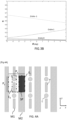
- FIG. 3B illustrates the diffraction efficiency of the diffractive optical element according to the first embodiment of the invention, for an incidence angle range between -5° and 5°.
- the width of the first band is 160nm
- a width of the second band is 61nm
- a length of the dotted line is 322nm.
- the relative position of the first band with respect to the second band is 186nm.
- the dimension Px of the pattern in the x direction is 465nm and the dimension Py of the sub-pattern in the y direction is 465nm.
- the efficiency of diffraction order -1 is higher than that of diffraction order +1 and much higher than that of diffraction order 0.
- the efficiency of diffraction order -1 is 55%, that of order +1 is 15% and that of diffraction order 0 is about 3%.
- the diffraction angle ⁇ d is 65°.
- the structure of the metasurface of the Figure 3A therefore allows the incident radiation to be redirected mainly towards diffraction order -1 while having a very low transmission of order 0.
- each sub-pattern E2 of the metasurface of the diffractive optical element comprises a disk C arranged between two successive dotted lines P of the first band M1.
- the first band M1 is therefore formed by an alternation of dotted lines and disks C in the y direction.
- the diameter of the disk C and its position relative to the dotted line P in the y direction in a sub-pattern E2 are optimized by RCWA simulation so as to generate an effective index adapted in the sub-pattern E2 relative to the effective index of the pattern E1,
- the efficiency of diffraction orders -1 and +1 is much higher than that of diffraction order 0.
- the efficiency of diffraction order -1 is 51%
- that of order +1 is 20%
- that of diffraction order 0 is less than 1%.
- the efficiency of diffraction order +1 is comparable to that of diffraction order -1.
- the diffraction angle ⁇ d is 65°.
- the structure of the metasurface of the Figure 4A therefore allows the incident radiation to be redirected mainly towards diffraction order -1 while having an extremely low transmission of order 0.
- the device D1 comprises at least one light source SL for emitting light radiation L in in the spectral range in which the substrate is transparent.
- the diffractive optical element is adapted so that light radiation emitted by the light source SL at the wavelength ⁇ is incident on the metasurface MS with the angle of incidence ⁇ i such that the light radiation diffracted L diff by said diffractive optical element is reflected in total internal reflection by the second face of the substrate and produces evanescent waves OE in at least one region of the second surface Se of the substrate.
- the device D1 further comprises a sample Ech placed in correspondence with at least one region of the second surface where said evanescent waves are produced and generating fluorescence radiation FI excited by said evanescent waves.
- the sample Ech is a cell culture sample, the cells being cultured on a slide in a material identical to that of the substrate SB and preserved in an aqueous medium.
- the diffraction angle ⁇ d of the diffracted radiation L diff being greater than the critical angle of total internal reflection between said substrate and water, the total internal reflection of the diffracted radiation at the interface between the second surface Se and the aqueous medium generates evanescent waves OE. These waves will excite fluorophores of the sample. located in a thin layer (about 100 nm) which contribute to the production of a fluorescence image
- the device D1 further comprises an objective Obj adapted to collect the fluorescence radiation FI and to direct it towards a detector Det adapted to detect said fluorescence radiation emitted by the sample.
- the diffracted radiation propagates over the entire length of the substrate and generates evanescent waves in each reflection region on a surface of the substrate. This means that when the dimension in the x direction of the substrate allows it, there are a plurality of reflection regions on a surface of the substrate where evanescent waves are produced and therefore a plurality of regions where fluorescence radiation within a sample can be excited.
- the transverse dimension (along the x and y directions) of the regions where the evanescent waves are produced is fixed by the smallest of the dimensions between the transverse dimension of the metasurface MS and the diameter of the beam of the incident radiation L in .
- the device D1 makes it possible to perform total internal reflection fluorescence microscopy (TIRF microscopy) of a sample Ech using a diffractive optical element 10 according to the invention.
- This diffractive optical element 10 makes it possible to generate a sufficient deviation of the incident radiation so that it propagates in the substrate of the diffractive optical element in a direction suitable for generating evanescent waves at the interface between the substrate of the diffractive optical element and the sample.
- the D1 device allows to selectively observe structures and processes localized on a cell membrane, with a spatial resolution in an axial direction much better than the diffraction limit.
- the D1 device enables TIRF microscopy to be performed without using a high numerical aperture ON objective, greatly reducing the cost of the D1 device compared to a prior art TIRF microscopy device.
- the path of the incident light radiation between the light source SL and the diffractive optical element is carried out in free space.
- the light source can be a laser source or an LED source placed in the immediate vicinity of the metasurface MS.
- the light source is an LED source placed in the immediate vicinity of the metasurface MS, it is advantageous to place the sample Ech above a region of the second surface Se of the substrate where evanescent waves are produced, which is transversely distant in the x direction from the metasurface MS.
- the intensity of the parasitic radiation emitted by the LED, diffused by the metasurface and illuminating the sample will be greatly reduced.
- the background noise produced by this parasitic radiation is reduced and the contrast is improved.
- the path of the incident light radiation between the light source SL and the diffractive optical element is fibered and the device D1 comprises a fiber optic coupler (not shown in the figure 5 ) to direct the light radiation L in towards the metasurface MS of the diffractive optical element.
- the SL light source is a laser source.
- the objective Obj is further adapted to collimate the incident radiation L in on the metasurface MS.
- the device comprises another lens (not shown) focusing the incident radiation L in emitted by the light source SL on the object focal plane of the objective Obj, the image of the radiation then being rejected to infinity in the image plane of the objective Obj.
- the angle of incidence ⁇ i of the incident radiation is adapted so that the reflected radiation L r is not collected by the objective.
- the diffractive optical element comprises a plurality of metasurfaces MS 1 , MS 2 , MS n , arranged on said first surface of the substrate Sm, with a dimension Px of the pattern in said direction x different for each metasurface.
- each metasurface is adapted to diffract light radiation L in of wavelength different from that of the other metasurfaces.
- the imaging device D1 of the figure 5 has the advantage of being wavelength tunable.
- Another subject of the invention is a device for detecting a biological sample by surface plasmon resonance D2 comprising a diffractive optical element according to the invention.
- a schematic view of the device D2 is illustrated by the figure 6 .
- the diffractive optical element of the device figure 6 comprises a plurality of n metasurfaces MS 1 , MS i , ..., MS n , with a dimension of said pattern Px along said direction x different for each metasurface, such that the diffracted radiation L diff reaches said second surface of the substrate Se at an angle ⁇ d , i associated with the i-th metasurface MS i .
- the device D2 of Fig. 6 further comprises at least one light source SL adapted to emit the light radiation L in in the spectral range in which the substrate is transparent.
- the source is adapted so that the light radiation is incident on the metasurfaces with the angle of incidence ⁇ i
- the layer to be analyzed is an aqueous layer.
- the sample Ech is arranged above the first substrate SB so that said diffracted radiation is reflected at least partially by the metal layer of the sample, forming reflected radiation L r .
- the diffractive optical element of the device D2 further comprises an optical coupling element MS out placed on the first surface of the substrate Sm and adapted to couple said light radiation reflected by the sample L r towards free space.
- the optical coupling element MS out comprises at least one output metasurface formed from the repetition of a periodic pattern E 1 along two directions x and y perpendicular to each other and parallel to a surface of the substrate, said pattern comprising a sub-pattern E 2 comprising a first portion of rectilinear strip along y P, said output metasurface arranged on said first surface of the substrate Sm the metasurface.
- the optical coupling element MS out is the “mirror” of the diffractive optical element MS in . That is to say that the optical element MS out is axially symmetrical by an axis parallel to the z direction of the diffractive optical element MS in .
- the D2 device of the figure 6 comprises a detector Det adapted to detect the intensity of said light radiation reflected by the sample and coupled to free space by said coupling element.
- the device D2 further comprises an objective Obj adapted to collect the reflected radiation L r coupled towards free space by said coupling element, and to direct it towards the detector Det.
- the diffractive optical element comprises at least one metasurface MS i adapted so that the diffraction angle ⁇ i associated with the metasurface produces, upon reflection on the metal surface, a resonant excitation of surface plasmons and an at least partial absorption of said diffracted radiation L diff .
- the incident radiation is deflected by a metasurface MS i with an associated diffraction angle ⁇ d , i , which allows the excitation of the surface plasmon resonance upon reflection by the metal layer Met, the diffracted radiation is partially absorbed and the intensity of the reflected radiation L r decreases.
- a layer of chemical functionalization adapted to allow the adsorption of specific biological molecules that it is desired to detect in the layer to be analyzed An.
- each metasurface MS In order to detect the presence of molecules, it is therefore necessary to illuminate, using the light source SL, each metasurface MS successively and to detect using the detector Det the intensity of the reflected radiation L r .
- ⁇ SPR, 0 the excitation angle of the surface plasmon resonance of the layer Met, without the presence of molecules to be detected in the layer to be analyzed An.
- the intensity of the reflected radiation L r is reduced compared to the intensity of the reflected radiation L r obtained with the other metasurfaces.
- the D2 device of the figure 6 allows biological detection by surface plasmon resonance with a significantly simplified assembly compared to prior art devices. More specifically, this device allows surface plasmon resonance detection without requiring variation of the wavelength or the angle of incidence ⁇ i of the incident radiation L in . In addition, this device is simple to align, unlike prior art devices which mostly use coupling prisms to excite surface plasmon resonance, the latter being bulky and complex to align.
Landscapes
- Physics & Mathematics (AREA)
- General Physics & Mathematics (AREA)
- Optics & Photonics (AREA)
- Health & Medical Sciences (AREA)
- Chemical & Material Sciences (AREA)
- Analytical Chemistry (AREA)
- Biochemistry (AREA)
- Life Sciences & Earth Sciences (AREA)
- Nuclear Medicine, Radiotherapy & Molecular Imaging (AREA)
- General Health & Medical Sciences (AREA)
- Immunology (AREA)
- Pathology (AREA)
- Investigating Or Analysing Materials By Optical Means (AREA)
- Microscoopes, Condenser (AREA)
- Diffracting Gratings Or Hologram Optical Elements (AREA)
- Lenses (AREA)
Claims (11)
- Beugungsoptisches Element (10), umfassend:- ein Substrat (SB) mit einer ersten Oberfläche (Sm) und einer zweiten Oberfläche gegenüber der ersten Oberfläche (Se), das für Licht in mindestens einem Spektralbereich transparent ist und in diesem Spektralbereich einen Brechungsindex aufweist, der höher als der von Wasser ist;- mindestens eine Metaoberfläche (MS), die aus einem dielektrischen Material besteht und auf der ersten Oberfläche des Substrats (Sm) angeordnet ist, wobei die Metaoberfläche aus der Wiederholung eines periodischen Musters (E1) in zwei Richtungen x und y, die senkrecht zueinander und parallel zu einer Oberfläche des Substrats verlaufen, gebildet ist, wobei das Muster ein Untermuster (E2) umfasst, das einen ersten geradlinigen Bandabschnitt (P) in der Richtung y umfasst;wobei die Metaoberfläche ein erstes Band (M1) aus gepunkteten Linien (P) in der Richtung y aufweist, das aus dem Untermuster gebildet ist;wobei das periodische Muster weiterhin einen zweiten geradlinigen Bandabschnitt in der Richtung y umfasst, sodass die Metaoberfläche ein zweites durchgehendes Band (M2) in einer Richtung y aufweist,wobei die Metaoberfläche dazu ausgelegt ist, dass sie Lichtstrahlung (Lin) mit einer im genannten Spektralbereich enthaltenen Wellenlänge λ, die mit einem Einfallswinkel einfällt, entlang einer gebeugten Strahlung (Ldiff) beugt, sodass sich die gebeugte Strahlung im Substrat ausbreitet und die zweite Oberfläche des Substrats (Se) unter einem gebeugten Winkel θd erreicht, der größer oder gleich einem Grenzwinkel θc der internen Gesamtbrechung zwischen dem Substrat und Wasser ist,wobei die Metaoberfläche so konfiguriert ist, dass sie für den Einfallswinkel eine Transmission der Beugungsordnung 0 von weniger als 5 % und eine Transmission der gebeugten Strahlung (Ldiff), die einer Beugungsordnung -1 oder +1 entspricht, von mehr als 50 % aufweist.
- Beugungsoptisches Element nach dem vorhergehenden Anspruch, wobei innerhalb des Musters die Fläche des ersten Bandes kleiner ist als die Fläche des zweiten Bandes und wobei eine Breite des ersten Bandes (I1) zwischen 30 nm und 500 nm beträgt, eine Breite des zweiten Bandes (12) zwischen 100 nm und 700 nm beträgt und eine Länge der gepunkteten Linie (P) zwischen 60 nm und 800 nm beträgt.
- Beugungsoptisches Element nach einem der Ansprüche 1 oder 2, wobei das Untermuster eine Scheibe (C) umfasst, wobei die Scheibe zwischen zwei aufeinanderfolgenden gepunkteten Linien (P) des ersten Bandes angeordnet ist.
- Beugungsoptisches Element nach einem der vorhergehenden Ansprüche, wobei die Abmessung des Musters (Px) in Richtung x derart ist, dass Px < λ/nWasser, wobei nWasser ein Brechungsindex von Wasser ist.
- Beugungsoptisches Element nach einem der vorhergehenden Ansprüche, wobei die Gesamtabmessung der Metaoberfläche in der Richtung x (xMS) derart ist, dass xMS < 2.e.sinθd, wobei e die Dicke des Substrats ist.
- Beugungsoptisches Element nach einem der vorhergehenden Ansprüche, wobei die Abmessung des Musters (Py) in Richtung y zwischen 300 nm und 1000 nm beträgt.
- Beugungsoptisches Element nach einem der vorhergehenden Ansprüche, wobei der Brechungsindex des Metaoberflächenmaterials größer ist als der Brechungsindex eines Substratmaterials.
- Beugungsoptisches Element nach einem der vorhergehenden Ansprüche, das eine Vielzahl von Metaoberflächen (MS1, MS2, MSn) umfasst, die auf der ersten Oberfläche des Substrats (Sm) angeordnet sind, wobei die Abmessung des Musters in der Richtung x (Px) für jede Metaoberfläche unterschiedlich ist, sodass jede Metaoberfläche dazu ausgelegt ist, Lichtstrahlung (Lin) mit der Wellenlänge, die in diesem Bereich enthalten ist und sich von der der anderen Metaoberflächen unterscheidet, zu beugen.
- Bildgebungsvorrichtung (D1) für eine Probe durch Totalreflexions-Fluoreszenzmikroskopie, umfassend ein beugungsoptisches Element (10) nach einem der vorhergehenden Ansprüche, die Folgendes umfasst:- mindestens eine Lichtquelle (SL), die dazu ausgelegt ist, die Lichtstrahlung (Lin) im genannten Spektralbereich, die auf das genannte beugungsoptische Element mit dem genannten Einfallswinkel einfällt, zu emittieren,
wobei die durch das beugungsoptische Element gebeugte Lichtstrahlung in mindestens einer Region der zweiten Oberfläche (Se) des Substrats evaneszente Wellen (OE) erzeugt;- eine Probe (Ech), die entsprechend mindestens einer Region der zweiten Oberfläche, in der die evaneszenten Wellen erzeugt werden, platziert ist und eine durch die evaneszenten Wellen angeregte Fluoreszenzstrahlung (Fl) erzeugt;- einen Detektor (Det), der dazu ausgelegt ist, die von der Probe emittierte Fluoreszenzstrahlung (Fl) zu erfassen. - Vorrichtung zur Erfassung (D2) einer biologischen Probe durch Oberflächenplasmonenresonanz, umfassend ein beugungsoptisches Element (10) nach einem der Ansprüche 1 bis 8,wobei das beugungsoptische Element umfasst:- eine Vielzahl von Metaoberflächen (MS1, MS2, MSn,) wobei eine Abmessung des Musters in der Richtung x (Px) bei jeder Metaoberfläche unterschiedlich ist, sodass die gebeugte Strahlung (Ldiff) die zweite Oberfläche des Substrats (Se) in einem Beugungswinkel θD erreicht, der bei jeder Metaoberfläche unterschiedlich ist,wobei die Vorrichtung weiterhin umfasst:- mindestens eine Lichtquelle (SL), die dazu ausgelegt ist, die Lichtstrahlung (Lin) im genannten Spektralbereich, die auf das genannte beugungsoptische Element mit dem genannten Einfallswinkel einfällt, zu emittieren,- eine Probe (Ech), die mindestens ein zweites Substrat (S2), eine über dem zweiten Substrat angeordnete metallische Schicht (Met) und eine über der Metallschicht angeordnete zu analysierenden Schicht (An) umfasst, wobei die Probe über dem ersten Substrat (SB) so angeordnet ist, dass die gebeugte Strahlung zumindest teilweise durch die metallische Schicht der Probe reflektiert wird (Lr);wobei das beugungsoptische Element ferner ein optisches Kopplungselement (MSout) umfasst, das dazu ausgelegt ist, die von der Probe reflektierte Lichtstrahlung in den freien Raum einzukoppeln;- einen Detektor (Det), der dazu ausgelegt ist, die Intensität der von der Probe reflektierten und durch das Kopplungselement in den freien Raum eingekoppelten Lichtstrahlung zu erfassen;mindestens eine Metaoberfläche, die so ausgelegt ist, dass der der Metaoberfläche zugeordnete Beugungswinkel bei Brechung an der metallischen Oberfläche eine resonante Anregung von Oberflächenplasmonen und eine zumindest partielle Absorption der gebeugten Strahlung (Ldiff) hervorruft.
- Vorrichtung nach dem vorhergehenden Anspruch, wobei das optische Kopplungselement mindestens eine Ausgangsmetaoberfläche umfasst, die aus der Wiederholung eines periodischen Musters (E1) in zwei Richtungen x und y, die senkrecht zueinander und parallel zu einer Oberfläche des Substrats verlaufen, gebildet wird, wobei das Muster ein Untermuster (E2) umfasst, das einen ersten Abschnitt eines geradlinigen, entlang y verlaufenden Bandes (P) umfasst, wobei die Ausgangsmetaoberfläche auf der ersten Oberfläche des Substrats (Sm) angeordnet ist.
Applications Claiming Priority (2)
| Application Number | Priority Date | Filing Date | Title |
|---|---|---|---|
| FR1912054A FR3102573B1 (fr) | 2019-10-28 | 2019-10-28 | Elément optique diffractif comprenant une métasurface pour la microscopie TIRF |
| PCT/EP2020/079768 WO2021083787A1 (fr) | 2019-10-28 | 2020-10-22 | Element optique diffractif comprenant une metasurface pour la microscopie tirf |
Publications (2)
| Publication Number | Publication Date |
|---|---|
| EP4052073A1 EP4052073A1 (de) | 2022-09-07 |
| EP4052073B1 true EP4052073B1 (de) | 2024-12-04 |
Family
ID=69630420
Family Applications (1)
| Application Number | Title | Priority Date | Filing Date |
|---|---|---|---|
| EP20792672.6A Active EP4052073B1 (de) | 2019-10-28 | 2020-10-22 | Diffraktives optisches element mit einer metaoberfläche für die tirf-mikroskopie |
Country Status (5)
| Country | Link |
|---|---|
| US (1) | US12455399B2 (de) |
| EP (1) | EP4052073B1 (de) |
| JP (1) | JP7532515B2 (de) |
| FR (1) | FR3102573B1 (de) |
| WO (1) | WO2021083787A1 (de) |
Families Citing this family (4)
| Publication number | Priority date | Publication date | Assignee | Title |
|---|---|---|---|---|
| CN114488525B (zh) * | 2022-04-15 | 2022-08-23 | 中国科学院光电技术研究所 | 一种超构表面成像系统、设计方法和探测器 |
| CN118226631B (zh) * | 2024-03-12 | 2025-07-04 | 南京理工大学 | 用于显微成像的等波长周期光栅纵向深度结构光照明发生器 |
| WO2025259172A1 (en) * | 2024-06-13 | 2025-12-18 | Chalmers Ventures Ab | A compact optical device for detecting and/or measuring particle or biomolecular interactions and a method for manufacturing such |
| WO2026048649A1 (ja) * | 2024-08-29 | 2026-03-05 | 国立大学法人東京科学大学 | 検出装置 |
Family Cites Families (9)
| Publication number | Priority date | Publication date | Assignee | Title |
|---|---|---|---|---|
| DE19516741C2 (de) * | 1995-05-06 | 1997-05-07 | Kurz Leonhard Fa | Beugungsoptisch wirksame Strukturanordnung |
| WO2010032157A1 (en) * | 2008-09-17 | 2010-03-25 | Koninklijke Philips Electronics N.V. | Wire-grid sensor with continuously controllable height of detection volume |
| JP5589656B2 (ja) * | 2009-12-11 | 2014-09-17 | セイコーエプソン株式会社 | センサーチップ、センサーカートリッジ及び分析装置 |
| WO2013033591A1 (en) * | 2011-08-31 | 2013-03-07 | President And Fellows Of Harvard College | Amplitude, phase and polarization plate for photonics |
| MA34792B1 (fr) * | 2012-06-28 | 2014-01-02 | Mascir Morrocan Foundation For Advanced Science Innovation & Res | Design d'un capteur à base de mode optiques guidés dans une micro puce à structure périodique de milieux diéléctriques à haute performance |
| US9989525B2 (en) * | 2013-03-15 | 2018-06-05 | Axela Inc. | Diffraction based biosensor containing two diffractive gratings |
| EP3321663B1 (de) * | 2015-07-07 | 2021-03-24 | Furuno Electric Co., Ltd. | Messchip, messvorrichtung und messverfahren |
| IL307294A (en) * | 2017-01-27 | 2023-11-01 | Magic Leap Inc | Diffraction gratings produced using a surface cell with differently oriented nanobeams |
| KR102909206B1 (ko) * | 2019-02-15 | 2026-01-06 | 삼성전자주식회사 | 다층 메타 렌즈 및 이를 포함하는 광학 장치 |
-
2019
- 2019-10-28 FR FR1912054A patent/FR3102573B1/fr active Active
-
2020
- 2020-10-22 WO PCT/EP2020/079768 patent/WO2021083787A1/fr not_active Ceased
- 2020-10-22 EP EP20792672.6A patent/EP4052073B1/de active Active
- 2020-10-22 US US17/771,801 patent/US12455399B2/en active Active
- 2020-10-22 JP JP2022524999A patent/JP7532515B2/ja active Active
Also Published As
| Publication number | Publication date |
|---|---|
| FR3102573B1 (fr) | 2024-12-13 |
| US20220381951A1 (en) | 2022-12-01 |
| FR3102573A1 (fr) | 2021-04-30 |
| US12455399B2 (en) | 2025-10-28 |
| EP4052073A1 (de) | 2022-09-07 |
| JP7532515B2 (ja) | 2024-08-13 |
| WO2021083787A1 (fr) | 2021-05-06 |
| JP2022554246A (ja) | 2022-12-28 |
Similar Documents
| Publication | Publication Date | Title |
|---|---|---|
| EP4052073B1 (de) | Diffraktives optisches element mit einer metaoberfläche für die tirf-mikroskopie | |
| EP2734884B1 (de) | Konoskopische optische beleuchtungsvorrichtung mit einem hohlen konus für ein optisches mikroskop und verfahren zur optischen mikroskopie in der konoskopie | |
| US10048200B2 (en) | Optical sensor based with multilayered plasmonic structure comprising a nanoporous metallic layer | |
| EP3503193B1 (de) | Bilderfassungssensor, der den empfang einer information über eine lichtwellenphase ermöglicht | |
| WO2018138223A1 (fr) | Détecteur optique de particules | |
| FR2942049A1 (fr) | Microscope de plasmon de surface a haute resolution comportant un interferometre heterodyne fibre | |
| GB2545157A (en) | Analysing apparatus and method | |
| EP2710351A2 (de) | Biochip-vorrichtung | |
| FR3052923A1 (fr) | Reflecteur optique resonant a multiples couches minces de materiaux dielectriques, capteur optique et dispositif d'amplification laser comportant un tel reflecteur | |
| EP3751258B1 (de) | Vorrichtung und verfahren zur beobachtung einer fluoreszenten probe | |
| WO2018150044A1 (fr) | Détecteur optique de particules | |
| FR2940450A1 (fr) | Dispositif et procede pour etudier une zone d'etude par onde acoustique | |
| WO2017207360A1 (fr) | Dispositif et procede d'eclairage pour microscopie de fluorescence a onde evanescente | |
| FR3126508A1 (fr) | Lame optique biocompatible destinée à la microscopie à réflexion totale interne et système d’imagerie microscopique comportant une telle lame | |
| EP4394487A1 (de) | Vorrichtung zur beobachtung einer probe mittels bildgebung | |
| FR3062913A1 (fr) | Procede de detection d'une variation locale d'indice de refraction d'un milieu dielectrique situe a la surface d'un capteur optique | |
| FR2915804A1 (fr) | Cellule spectroscopique a double paire de lentille | |
| FR3052914A1 (fr) | Capteur optique comportant un reflecteur optique resonant a multiples couches minces de materiaux dielectriques | |
| FR3146214A1 (fr) | Lame optique destinée à la microscopie par réflexion totale interne, dispositif de microscopie par réflexion totale interne comportant une telle lame et procédé de fabrication d’une telle lame | |
| Sieben-Xu et al. | High performance surface plasmon resonance sensor based on two dimensional ultra-thin metal nanoslit arrays | |
| Stark | Studies of the resonant interaction of photons with surface plasmons and sub-wavelength apertures in metallo-dielectric structures | |
| EP3575774A1 (de) | Vorrichtung und verfahren zur beobachtung von teilchen, insbesondere teilchen im submikrometerbereich | |
| WO2004086012A1 (fr) | Dispositif de mesure de fluorescence d’une pluralite de zones a observer |
Legal Events
| Date | Code | Title | Description |
|---|---|---|---|
| STAA | Information on the status of an ep patent application or granted ep patent |
Free format text: STATUS: UNKNOWN |
|
| STAA | Information on the status of an ep patent application or granted ep patent |
Free format text: STATUS: THE INTERNATIONAL PUBLICATION HAS BEEN MADE |
|
| PUAI | Public reference made under article 153(3) epc to a published international application that has entered the european phase |
Free format text: ORIGINAL CODE: 0009012 |
|
| STAA | Information on the status of an ep patent application or granted ep patent |
Free format text: STATUS: REQUEST FOR EXAMINATION WAS MADE |
|
| 17P | Request for examination filed |
Effective date: 20220503 |
|
| AK | Designated contracting states |
Kind code of ref document: A1 Designated state(s): AL AT BE BG CH CY CZ DE DK EE ES FI FR GB GR HR HU IE IS IT LI LT LU LV MC MK MT NL NO PL PT RO RS SE SI SK SM TR |
|
| DAV | Request for validation of the european patent (deleted) | ||
| DAX | Request for extension of the european patent (deleted) | ||
| GRAP | Despatch of communication of intention to grant a patent |
Free format text: ORIGINAL CODE: EPIDOSNIGR1 |
|
| STAA | Information on the status of an ep patent application or granted ep patent |
Free format text: STATUS: GRANT OF PATENT IS INTENDED |
|
| INTG | Intention to grant announced |
Effective date: 20240625 |
|
| GRAS | Grant fee paid |
Free format text: ORIGINAL CODE: EPIDOSNIGR3 |
|
| GRAA | (expected) grant |
Free format text: ORIGINAL CODE: 0009210 |
|
| STAA | Information on the status of an ep patent application or granted ep patent |
Free format text: STATUS: THE PATENT HAS BEEN GRANTED |
|
| AK | Designated contracting states |
Kind code of ref document: B1 Designated state(s): AL AT BE BG CH CY CZ DE DK EE ES FI FR GB GR HR HU IE IS IT LI LT LU LV MC MK MT NL NO PL PT RO RS SE SI SK SM TR |
|
| REG | Reference to a national code |
Ref country code: CH Ref legal event code: EP |
|
| REG | Reference to a national code |
Ref country code: DE Ref legal event code: R096 Ref document number: 602020042595 Country of ref document: DE |
|
| REG | Reference to a national code |
Ref country code: IE Ref legal event code: FG4D Free format text: LANGUAGE OF EP DOCUMENT: FRENCH |
|
| REG | Reference to a national code |
Ref country code: LT Ref legal event code: MG9D |
|
| REG | Reference to a national code |
Ref country code: NL Ref legal event code: MP Effective date: 20241204 |
|
| PG25 | Lapsed in a contracting state [announced via postgrant information from national office to epo] |
Ref country code: HR Free format text: LAPSE BECAUSE OF FAILURE TO SUBMIT A TRANSLATION OF THE DESCRIPTION OR TO PAY THE FEE WITHIN THE PRESCRIBED TIME-LIMIT Effective date: 20241204 |
|
| PG25 | Lapsed in a contracting state [announced via postgrant information from national office to epo] |
Ref country code: FI Free format text: LAPSE BECAUSE OF FAILURE TO SUBMIT A TRANSLATION OF THE DESCRIPTION OR TO PAY THE FEE WITHIN THE PRESCRIBED TIME-LIMIT Effective date: 20241204 |
|
| PG25 | Lapsed in a contracting state [announced via postgrant information from national office to epo] |
Ref country code: BG Free format text: LAPSE BECAUSE OF FAILURE TO SUBMIT A TRANSLATION OF THE DESCRIPTION OR TO PAY THE FEE WITHIN THE PRESCRIBED TIME-LIMIT Effective date: 20241204 |
|
| PG25 | Lapsed in a contracting state [announced via postgrant information from national office to epo] |
Ref country code: ES Free format text: LAPSE BECAUSE OF FAILURE TO SUBMIT A TRANSLATION OF THE DESCRIPTION OR TO PAY THE FEE WITHIN THE PRESCRIBED TIME-LIMIT Effective date: 20241204 |
|
| PG25 | Lapsed in a contracting state [announced via postgrant information from national office to epo] |
Ref country code: NO Free format text: LAPSE BECAUSE OF FAILURE TO SUBMIT A TRANSLATION OF THE DESCRIPTION OR TO PAY THE FEE WITHIN THE PRESCRIBED TIME-LIMIT Effective date: 20250304 |
|
| PG25 | Lapsed in a contracting state [announced via postgrant information from national office to epo] |
Ref country code: GR Free format text: LAPSE BECAUSE OF FAILURE TO SUBMIT A TRANSLATION OF THE DESCRIPTION OR TO PAY THE FEE WITHIN THE PRESCRIBED TIME-LIMIT Effective date: 20250305 Ref country code: LV Free format text: LAPSE BECAUSE OF FAILURE TO SUBMIT A TRANSLATION OF THE DESCRIPTION OR TO PAY THE FEE WITHIN THE PRESCRIBED TIME-LIMIT Effective date: 20241204 |
|
| PG25 | Lapsed in a contracting state [announced via postgrant information from national office to epo] |
Ref country code: RS Free format text: LAPSE BECAUSE OF FAILURE TO SUBMIT A TRANSLATION OF THE DESCRIPTION OR TO PAY THE FEE WITHIN THE PRESCRIBED TIME-LIMIT Effective date: 20250304 |
|
| PG25 | Lapsed in a contracting state [announced via postgrant information from national office to epo] |
Ref country code: NL Free format text: LAPSE BECAUSE OF FAILURE TO SUBMIT A TRANSLATION OF THE DESCRIPTION OR TO PAY THE FEE WITHIN THE PRESCRIBED TIME-LIMIT Effective date: 20241204 |
|
| REG | Reference to a national code |
Ref country code: AT Ref legal event code: MK05 Ref document number: 1748743 Country of ref document: AT Kind code of ref document: T Effective date: 20241204 |
|
| PG25 | Lapsed in a contracting state [announced via postgrant information from national office to epo] |
Ref country code: SM Free format text: LAPSE BECAUSE OF FAILURE TO SUBMIT A TRANSLATION OF THE DESCRIPTION OR TO PAY THE FEE WITHIN THE PRESCRIBED TIME-LIMIT Effective date: 20241204 |
|
| PG25 | Lapsed in a contracting state [announced via postgrant information from national office to epo] |
Ref country code: PL Free format text: LAPSE BECAUSE OF FAILURE TO SUBMIT A TRANSLATION OF THE DESCRIPTION OR TO PAY THE FEE WITHIN THE PRESCRIBED TIME-LIMIT Effective date: 20241204 |
|
| PG25 | Lapsed in a contracting state [announced via postgrant information from national office to epo] |
Ref country code: IS Free format text: LAPSE BECAUSE OF FAILURE TO SUBMIT A TRANSLATION OF THE DESCRIPTION OR TO PAY THE FEE WITHIN THE PRESCRIBED TIME-LIMIT Effective date: 20250404 |
|
| PG25 | Lapsed in a contracting state [announced via postgrant information from national office to epo] |
Ref country code: PT Free format text: LAPSE BECAUSE OF FAILURE TO SUBMIT A TRANSLATION OF THE DESCRIPTION OR TO PAY THE FEE WITHIN THE PRESCRIBED TIME-LIMIT Effective date: 20250404 |
|
| PG25 | Lapsed in a contracting state [announced via postgrant information from national office to epo] |
Ref country code: EE Free format text: LAPSE BECAUSE OF FAILURE TO SUBMIT A TRANSLATION OF THE DESCRIPTION OR TO PAY THE FEE WITHIN THE PRESCRIBED TIME-LIMIT Effective date: 20241204 |
|
| PG25 | Lapsed in a contracting state [announced via postgrant information from national office to epo] |
Ref country code: AT Free format text: LAPSE BECAUSE OF FAILURE TO SUBMIT A TRANSLATION OF THE DESCRIPTION OR TO PAY THE FEE WITHIN THE PRESCRIBED TIME-LIMIT Effective date: 20241204 Ref country code: RO Free format text: LAPSE BECAUSE OF FAILURE TO SUBMIT A TRANSLATION OF THE DESCRIPTION OR TO PAY THE FEE WITHIN THE PRESCRIBED TIME-LIMIT Effective date: 20241204 |
|
| PG25 | Lapsed in a contracting state [announced via postgrant information from national office to epo] |
Ref country code: SK Free format text: LAPSE BECAUSE OF FAILURE TO SUBMIT A TRANSLATION OF THE DESCRIPTION OR TO PAY THE FEE WITHIN THE PRESCRIBED TIME-LIMIT Effective date: 20241204 |
|
| PG25 | Lapsed in a contracting state [announced via postgrant information from national office to epo] |
Ref country code: CZ Free format text: LAPSE BECAUSE OF FAILURE TO SUBMIT A TRANSLATION OF THE DESCRIPTION OR TO PAY THE FEE WITHIN THE PRESCRIBED TIME-LIMIT Effective date: 20241204 |
|
| PG25 | Lapsed in a contracting state [announced via postgrant information from national office to epo] |
Ref country code: IT Free format text: LAPSE BECAUSE OF FAILURE TO SUBMIT A TRANSLATION OF THE DESCRIPTION OR TO PAY THE FEE WITHIN THE PRESCRIBED TIME-LIMIT Effective date: 20241204 |
|
| REG | Reference to a national code |
Ref country code: DE Ref legal event code: R097 Ref document number: 602020042595 Country of ref document: DE |
|
| PG25 | Lapsed in a contracting state [announced via postgrant information from national office to epo] |
Ref country code: SE Free format text: LAPSE BECAUSE OF FAILURE TO SUBMIT A TRANSLATION OF THE DESCRIPTION OR TO PAY THE FEE WITHIN THE PRESCRIBED TIME-LIMIT Effective date: 20241204 |
|
| PG25 | Lapsed in a contracting state [announced via postgrant information from national office to epo] |
Ref country code: DK Free format text: LAPSE BECAUSE OF FAILURE TO SUBMIT A TRANSLATION OF THE DESCRIPTION OR TO PAY THE FEE WITHIN THE PRESCRIBED TIME-LIMIT Effective date: 20241204 |
|
| PLBE | No opposition filed within time limit |
Free format text: ORIGINAL CODE: 0009261 |
|
| STAA | Information on the status of an ep patent application or granted ep patent |
Free format text: STATUS: NO OPPOSITION FILED WITHIN TIME LIMIT |
|
| 26N | No opposition filed |
Effective date: 20250905 |
|
| PGFP | Annual fee paid to national office [announced via postgrant information from national office to epo] |
Ref country code: DE Payment date: 20251126 Year of fee payment: 6 |
|
| PGFP | Annual fee paid to national office [announced via postgrant information from national office to epo] |
Ref country code: GB Payment date: 20251029 Year of fee payment: 6 |
|
| PGFP | Annual fee paid to national office [announced via postgrant information from national office to epo] |
Ref country code: FR Payment date: 20251030 Year of fee payment: 6 |