EP4053741A2 - Ensemble imprimante avec détection d'étiquettes d'identification par radiofréquence (rfid) à petit pas - Google Patents
Ensemble imprimante avec détection d'étiquettes d'identification par radiofréquence (rfid) à petit pas Download PDFInfo
- Publication number
- EP4053741A2 EP4053741A2 EP22159082.1A EP22159082A EP4053741A2 EP 4053741 A2 EP4053741 A2 EP 4053741A2 EP 22159082 A EP22159082 A EP 22159082A EP 4053741 A2 EP4053741 A2 EP 4053741A2
- Authority
- EP
- European Patent Office
- Prior art keywords
- media
- rfid
- shield
- inlay
- printer assembly
- Prior art date
- Legal status (The legal status is an assumption and is not a legal conclusion. Google has not performed a legal analysis and makes no representation as to the accuracy of the status listed.)
- Granted
Links
Images


Classifications
-
- G—PHYSICS
- G06—COMPUTING OR CALCULATING; COUNTING
- G06K—GRAPHICAL DATA READING; PRESENTATION OF DATA; RECORD CARRIERS; HANDLING RECORD CARRIERS
- G06K19/00—Record carriers for use with machines and with at least a part designed to carry digital markings
- G06K19/06—Record carriers for use with machines and with at least a part designed to carry digital markings characterised by the kind of the digital marking, e.g. shape, nature, code
- G06K19/067—Record carriers with conductive marks, printed circuits or semiconductor circuit elements, e.g. credit or identity cards also with resonating or responding marks without active components
- G06K19/07—Record carriers with conductive marks, printed circuits or semiconductor circuit elements, e.g. credit or identity cards also with resonating or responding marks without active components with integrated circuit chips
- G06K19/077—Constructional details, e.g. mounting of circuits in the carrier
- G06K19/07749—Constructional details, e.g. mounting of circuits in the carrier the record carrier being capable of non-contact communication, e.g. constructional details of the antenna of a non-contact smart card
- G06K19/07773—Antenna details
-
- G—PHYSICS
- G06—COMPUTING OR CALCULATING; COUNTING
- G06K—GRAPHICAL DATA READING; PRESENTATION OF DATA; RECORD CARRIERS; HANDLING RECORD CARRIERS
- G06K17/00—Methods or arrangements for effecting co-operative working between equipments covered by two or more of main groups G06K1/00 - G06K15/00, e.g. automatic card files incorporating conveying and reading operations
- G06K17/0022—Methods or arrangements for effecting co-operative working between equipments covered by two or more of main groups G06K1/00 - G06K15/00, e.g. automatic card files incorporating conveying and reading operations arrangements or provisions for transferring data to distant stations, e.g. from a sensing device
- G06K17/0025—Methods or arrangements for effecting co-operative working between equipments covered by two or more of main groups G06K1/00 - G06K15/00, e.g. automatic card files incorporating conveying and reading operations arrangements or provisions for transferring data to distant stations, e.g. from a sensing device the arrangement consisting of a wireless interrogation device in combination with a device for optically marking the record carrier
-
- G—PHYSICS
- G06—COMPUTING OR CALCULATING; COUNTING
- G06K—GRAPHICAL DATA READING; PRESENTATION OF DATA; RECORD CARRIERS; HANDLING RECORD CARRIERS
- G06K7/00—Methods or arrangements for sensing record carriers, e.g. for reading patterns
- G06K7/10—Methods or arrangements for sensing record carriers, e.g. for reading patterns by electromagnetic radiation, e.g. optical sensing; by corpuscular radiation
- G06K7/10009—Methods or arrangements for sensing record carriers, e.g. for reading patterns by electromagnetic radiation, e.g. optical sensing; by corpuscular radiation sensing by radiation using wavelengths larger than 0.1 mm, e.g. radio-waves or microwaves
- G06K7/10366—Methods or arrangements for sensing record carriers, e.g. for reading patterns by electromagnetic radiation, e.g. optical sensing; by corpuscular radiation sensing by radiation using wavelengths larger than 0.1 mm, e.g. radio-waves or microwaves the interrogation device being adapted for miscellaneous applications
- G06K7/10415—Methods or arrangements for sensing record carriers, e.g. for reading patterns by electromagnetic radiation, e.g. optical sensing; by corpuscular radiation sensing by radiation using wavelengths larger than 0.1 mm, e.g. radio-waves or microwaves the interrogation device being adapted for miscellaneous applications the interrogation device being fixed in its position, such as an access control device for reading wireless access cards, or a wireless ATM
- G06K7/10425—Methods or arrangements for sensing record carriers, e.g. for reading patterns by electromagnetic radiation, e.g. optical sensing; by corpuscular radiation sensing by radiation using wavelengths larger than 0.1 mm, e.g. radio-waves or microwaves the interrogation device being adapted for miscellaneous applications the interrogation device being fixed in its position, such as an access control device for reading wireless access cards, or a wireless ATM the interrogation device being arranged for interrogation of record carriers passing by the interrogation device
- G06K7/10435—Methods or arrangements for sensing record carriers, e.g. for reading patterns by electromagnetic radiation, e.g. optical sensing; by corpuscular radiation sensing by radiation using wavelengths larger than 0.1 mm, e.g. radio-waves or microwaves the interrogation device being adapted for miscellaneous applications the interrogation device being fixed in its position, such as an access control device for reading wireless access cards, or a wireless ATM the interrogation device being arranged for interrogation of record carriers passing by the interrogation device the interrogation device being positioned close to a conveyor belt or the like on which moving record carriers are passing
- G06K7/10455—Methods or arrangements for sensing record carriers, e.g. for reading patterns by electromagnetic radiation, e.g. optical sensing; by corpuscular radiation sensing by radiation using wavelengths larger than 0.1 mm, e.g. radio-waves or microwaves the interrogation device being adapted for miscellaneous applications the interrogation device being fixed in its position, such as an access control device for reading wireless access cards, or a wireless ATM the interrogation device being arranged for interrogation of record carriers passing by the interrogation device the interrogation device being positioned close to a conveyor belt or the like on which moving record carriers are passing the record carriers being fixed to an endless tape or at least not fixed to further objects
-
- B—PERFORMING OPERATIONS; TRANSPORTING
- B41—PRINTING; LINING MACHINES; TYPEWRITERS; STAMPS
- B41J—TYPEWRITERS; SELECTIVE PRINTING MECHANISMS, i.e. MECHANISMS PRINTING OTHERWISE THAN FROM A FORME; CORRECTION OF TYPOGRAPHICAL ERRORS
- B41J29/00—Details of, or accessories for, typewriters or selective printing mechanisms not otherwise provided for
- B41J29/38—Drives, motors, controls or automatic cut-off devices for the entire printing mechanism
- B41J29/393—Devices for controlling or analysing the entire machine ; Controlling or analysing mechanical parameters involving printing of test patterns
-
- B—PERFORMING OPERATIONS; TRANSPORTING
- B41—PRINTING; LINING MACHINES; TYPEWRITERS; STAMPS
- B41J—TYPEWRITERS; SELECTIVE PRINTING MECHANISMS, i.e. MECHANISMS PRINTING OTHERWISE THAN FROM A FORME; CORRECTION OF TYPOGRAPHICAL ERRORS
- B41J3/00—Typewriters or selective printing or marking mechanisms characterised by the purpose for which they are constructed
- B41J3/407—Typewriters or selective printing or marking mechanisms characterised by the purpose for which they are constructed for marking on special material
- B41J3/4075—Tape printers; Label printers
-
- B—PERFORMING OPERATIONS; TRANSPORTING
- B41—PRINTING; LINING MACHINES; TYPEWRITERS; STAMPS
- B41J—TYPEWRITERS; SELECTIVE PRINTING MECHANISMS, i.e. MECHANISMS PRINTING OTHERWISE THAN FROM A FORME; CORRECTION OF TYPOGRAPHICAL ERRORS
- B41J3/00—Typewriters or selective printing or marking mechanisms characterised by the purpose for which they are constructed
- B41J3/44—Typewriters or selective printing mechanisms having dual functions or combined with, or coupled to, apparatus performing other functions
- B41J3/50—Mechanisms producing characters by printing and also producing a record by other means, e.g. printer combined with RFID writer
-
- B—PERFORMING OPERATIONS; TRANSPORTING
- B65—CONVEYING; PACKING; STORING; HANDLING THIN OR FILAMENTARY MATERIAL
- B65C—LABELLING OR TAGGING MACHINES, APPARATUS, OR PROCESSES
- B65C11/00—Manually-controlled or manually-operable label dispensers, e.g. modified for the application of labels to articles
- B65C11/02—Manually-controlled or manually-operable label dispensers, e.g. modified for the application of labels to articles having printing equipment
-
- G—PHYSICS
- G06—COMPUTING OR CALCULATING; COUNTING
- G06K—GRAPHICAL DATA READING; PRESENTATION OF DATA; RECORD CARRIERS; HANDLING RECORD CARRIERS
- G06K19/00—Record carriers for use with machines and with at least a part designed to carry digital markings
- G06K19/06—Record carriers for use with machines and with at least a part designed to carry digital markings characterised by the kind of the digital marking, e.g. shape, nature, code
- G06K19/067—Record carriers with conductive marks, printed circuits or semiconductor circuit elements, e.g. credit or identity cards also with resonating or responding marks without active components
- G06K19/07—Record carriers with conductive marks, printed circuits or semiconductor circuit elements, e.g. credit or identity cards also with resonating or responding marks without active components with integrated circuit chips
- G06K19/073—Special arrangements for circuits, e.g. for protecting identification code in memory
- G06K19/07309—Means for preventing undesired reading or writing from or onto record carriers
- G06K19/07318—Means for preventing undesired reading or writing from or onto record carriers by hindering electromagnetic reading or writing
-
- B—PERFORMING OPERATIONS; TRANSPORTING
- B65—CONVEYING; PACKING; STORING; HANDLING THIN OR FILAMENTARY MATERIAL
- B65C—LABELLING OR TAGGING MACHINES, APPARATUS, OR PROCESSES
- B65C9/00—Details of labelling machines or apparatus
- B65C2009/0003—Use of RFID labels
Definitions
- Exemplary embodiments of the present disclosure relate generally to radio frequency identification (RFID) and, more particularly, to encoding an RFID inlay.
- RFID radio frequency identification
- Applicant has identified a number of deficiencies and problems associated with conventional RFID printers. Through applied effort, ingenuity, and innovation, many of these identified problems have been solved by developing solutions that are included in embodiments of the present disclosure, many examples of which are described in detail herein.
- a printer assembly that includes a media hub configured to receive a media roll and supply a media from the media roll along a media path.
- the media includes a plurality of labels, with each label of the plurality of labels comprising a Radio Frequency Identification (RFID) inlay.
- RFID Radio Frequency Identification
- the printer assembly also includes a media guide positioned adjacent to the media path.
- the media guide includes an RFID antenna.
- the RFID antenna is communicatively coupled to an RFID control system and configured to transmit signals to encode the RFID inlay on a first label of the plurality of labels.
- the media guide also includes at least one shield. The at least one shield is positioned adjacent to the RFID antenna to prevent, during an encoding of the RFID inlay on the first label of the plurality of labels, an encoding of the RFID inlay on a second label of the plurality of labels.
- the at least one shield comprises a material capable of absorbing electromagnetic signals.
- the material is copper.
- the media guide comprises a material allowing the signals transmitted by the RFID antenna to pass through the media guide.
- the material of the media guide is plastic.
- the material of the media guide is transparent.
- the at least one shield is configured to be removable from the media guide. In some embodiments, the at least one shield is configured to be attached to the media guide at more than one position. In some embodiments, the media guide defines a plane extending outward from a wall of a housing of a printer. In some embodiments, the media guide comprises a first shield positioned downstream from the RFID antenna and a second shield positioned upstream from the RFID antenna.
- a printer assembly in other various embodiments, includes a media guide positioned adjacent to a media path.
- the media guide includes an RFID antenna communicatively coupled to an RFID control system and configured to transmit signals to encode an RFID inlay on a media along the media path.
- the media guide also includes at least one shield positioned to prevent, during an encoding of the RFID inlay, an encoding of a second RFID inlay on the media.
- the at least one shield comprises a material capable of absorbing electromagnetic signals.
- the material is copper.
- the media guide comprises a material allowing the signals transmitted by the RFID antenna to pass through the media guide.
- the material of the media guide is plastic.
- the material of the media guide is transparent.
- the at least one shield is configured to be removable from the media guide. In some embodiments, the at least one shield is configured to be attached to the media guide at more than one position. In some embodiments, the media guide defines a plane extending outward from a wall of a housing of a printer. In some embodiments, the media guide comprises a first shield positioned downstream from the RFID antenna and a second shield positioned upstream from the RFID antenna.
- a media guide configured to be coupled to a housing of a printer.
- the media guide includes an RFID antenna configured to transmit signals to encode an RFID inlay.
- the media guide also includes at least one shield positioned adjacent to the RFID antenna.
- component or feature may,” “can,” “could,” “should,” “would,” “preferably,” “possibly,” “typically,” “optionally,” “for example,” “often,” or “might” (or other such language) be included or have a characteristic, that particular component or feature is not required to be included or to have the characteristic. Such component or feature may be optionally included in some embodiments, or it may be excluded.
- RFID radio frequency identification
- RFID inlay is used herein to correspond to an RFID tag that includes an integrated circuit (IC), an antenna element, and a substrate.
- the antenna element and the IC are fabricated on the substrate.
- the IC is communicatively coupled to the antenna element through an interconnect on the substrate.
- the integrated circuit in the RFID inlay may be configured to store encoded information or the encoded data.
- the RFID inlay may be configured to operate in various RF frequency bands such as, but not limited to, 13.56 MHz (hereinafter High Frequency Band) or 860 MHz-960 MHz (UHF band).
- the RFID inlay may have a dedicated power source that may enable the RFID inlay to communicate with one or more components, such as an RFID encoder and an RFID reader. Such RFID inlays are referred to as active RFID inlays.
- the RFID inlay may not have a dedicated power source.
- the RFID inlay may have a power coupler that is capable of inducing electrical charge when the RFID inlay is brought in an RF field. The induced electrical charge is thereafter used to power the RFID inlay itself.
- the word "media” is used herein to mean a printable medium, such as a page or paper, on which content, such as graphics, text, and/or visual images, may be printable.
- the media may correspond to a continuous media that may be loaded in an RFID printer in form of a roll or a stack, or may correspond to media that may be divided into a plurality of labels through perforations defined along a width of the media.
- the media may be divided into the plurality of labels through one or more marks that are defined at a predetermined distance from each other, along the length of the media.
- a contiguous stretch of the media, between two consecutive marks or two consecutive perforations corresponds to a label of the media.
- each label of the plurality of labels includes a corresponding RFID inlay.
- an RFID printer that is capable of encoding an RFID inlay provided on a plurality of labels in a media.
- the RFID printer defines a media travel path along which media in the RFID printer traverses.
- the media includes a plurality of labels, and each label of the plurality of labels further includes an RFID inlay.
- the RFID printer may facilitate traversal of the media along the media path so as to encode RFID inlay in at least one of the plurality of labels.
- the RFID printer comprises an RFID antenna, positioned adjacent to the media path, that is configured to transmit a signal to encode the RFID inlay provided on each of the plurality of labels. Because the RFID antenna is positioned adjacent to the media path, the RFID antenna facilitates encoding the RFID inlay on the plurality of labels while the media traverses along the media path.
- the RFID antenna is coupled to a media guide.
- the media guide is positioned adjacent to the media path and is configured to guide the media along the media path and prevent the media from skewing as the media traverses along the media path.
- the RFID antenna may be positioned adjacent to a media hub, a print head engine, and/or other structures along the media path
- a media sensor To encode the RFID inlay on a label of the plurality of labels while the media traverses along the media path, a media sensor generates an input signal as the media traverses along the media path. Based on the input signal, a processor in the RFID printer may be configured to determine a real-time location of the label (that includes the RFID inlay to be encoded). In some examples, after determining the real-time location of the label, the processor may instruct an RFID control system to encode the RFID inlay on the label by transmitting a signal through the RFID antenna. Because the RFID printer according to the various embodiments encodes the RFID inlay as the media traverses along the media path, there is no need to halt the traversal of the media in order to enable the RFID antenna to encode the RFID inlay.
- errors may arise during an encoding of an RFID inlay on a media having a small pitch.
- the term "pitch" describes a distance from a leading edge of an RFID inlay to a leading edge of the RFID inlay of the next adjacent label on the media.
- the RFID inlays are positioned close (e.g., less than one inch, in some examples, less than 0.5 inch, and in other examples, less than 0.1 inch) together.
- Media having a small pitch may be desirable for purposes of cost-savings as well as inclusion of additional labels and RFID inlays on the media.
- an RFID antenna may not be able to accurately encode information to a given RFID inlay while the media having a small pitch traverses the media path. That is, if there is a target RFID inlay, an upstream RFID inlay, and a downstream RFID inlay, each of these multiple RFID inlays may be detected simultaneously by the RFID antenna. This may result in errors such as an encoding of multiple RFID inlays at once (e.g., each of the target RFID inlay, upstream RFID inlay, and downstream RFID inlay, resulting in portions of information missing from the encoded RFID inlays, or may result in the RFID antenna not encoding any RFID labels as multiple RFID inlays are continuously simultaneously detected as the media traverses the media path.
- Various example embodiments disclosed herein are configured to comprise a media guide comprising at least one shield, such as a shield that is configured to shield an upstream or downstream RFID inlay from receiving an encoding signal. That is, the at least one shield is positioned adjacent to the RFID antenna to prevent, during an encoding of an RFID inlay on a first label of the plurality of labels, an encoding of the RFID inlay on a label upstream and on a label downstream from the first label.
- the at least one shield is configured to absorb radio and/or other electromagnetic waves during an encoding process of an RFID label that would otherwise encode one or more additional RFID inlays.
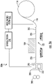
- FIGS. 1A-1C illustrate an example RFID printer 100, according to the one or more embodiments described herein.
- the RFID printer 100 may include a media hub 102, an RFID antenna 104 (described further below in conjunction with FIG. 2A-B ), an RFID control system 105, and a media output slot 106.
- the RFID printer 100 may include a ribbon drive assembly 108, a ribbon take-up hub 110, and a print head 112.
- the media hub is configured to receive a media roll 114.
- the media roll 114 may correspond to a roll of a media 116 that may have a plurality of labels 118.
- FIG. 1A illustrates example labels 118a, 118b, 118c, and 118d, for example.
- the plurality of labels 118 may be defined on the media 116 by means of perforations 120.
- the plurality of labels 118 may be defined on the media 116 by means of one or more marks (not shown).
- the media hub 102 may be coupled to a first electrical drive (not shown) that actuates the media hub 102. On actuation, the media hub 102 causes the media roll 114 to rotate, which further causes the media 116 to travel/traverse along a media path 122 (as shown in the shaded portion in FIG. 1B ).
- the scope of the disclosure is not limited to the media hub 102 facilitating supply of the media 116 along the media path 122.
- the RFID printer 100 may further include a platen roller (an example platen roller is further described in FIG. 2A ), in addition to the media hub 102, that may be positioned along the media path 122.
- the platen roller may be coupled to the first electrical drive, which actuates the platen roller.
- the platen roller may be configured to pull the media 116 from the media roll 114 (mounted on the media hub 102), causing the media 116 to travel along the media path 122.
- the first electrical drive may be coupled to both the platen roller and the media hub 102 such that both the platen roller and the media hub 102 operate in sync.
- Such configuration of the RFID printer 100 (that includes the platen roller and the media hub 102) is further described in conjunction with FIG. 2A .
- the RFID antenna 104 corresponds to an antenna element that is positioned adjacent to the media path 122.
- the RFID antenna 104 is coupled to a media guide 250 (described further below in conjunction with FIG. 2A-D ).
- the RFID antenna 104 may facilitate encoding of an RFID inlay 126 provided on each of the plurality of labels 118 (on the media 116), while the media traverses along the media path 122.
- the RFID control system 105 may include suitable logic and circuitry to control the operation of at least the RFID antenna 104.
- the RFID control system 105 includes an RFID encoder and an RFID reader that may cause the RFID antenna 104 to encode and read the RFID inlay 126, respectively.
- the structure and operation of the RFID control system 105 has been described in conjunction with FIG. 3 .
- the RFID control system 105 causes the RFID antenna 104 to encode the RFID inlay 126 on one of the labels 118 of the plurality of labels while the media 116 traverses along the media path 122. Therefore, subsequent to the encoding of the RFID inlay 126, the encoded RFID inlay 126 is outputted from the media output slot 106.
- the media output slot 106 corresponds to a slot in a housing of the RFID printer 100, through which the label 118 with an encoded RFID inlay 126 is outputted.
- the RFID printer 100 may print content on the labels 118.
- the RFID printer 100 may further include the ribbon drive assembly 108, the ribbon take-up hub 110, and the print head 112.
- the ribbon drive assembly 108 may receive a ribbon roll 128 that corresponds to a roll of a ribbon 130.
- the ribbon 130 may correspond to an ink media that is utilized to dispose ink onto the media 116 to print content on the media 116 ( e.g., label 118).
- the ribbon drive assembly 108 may be coupled to a third electrical drive that may be configured to actuate the ribbon drive assembly 108.
- the ribbon drive assembly 108 rotates, which in turn causes the ribbon roll 128 to rotate and supply the ribbon 130 along a ribbon path 132 (as shown in the shaded in FIG. 1C ).
- the ribbon 130 traverses from the ribbon drive assembly 108 to the print head 112 and further to the ribbon take-up hub 110.
- the ribbon take-up hub 110 may correspond to an assembly that may receive used ribbon (i.e., a section of the ribbon 130 from which the ink has been is disposed on the media 116).
- the ribbon take-up hub 110 may also be coupled to the third electrical drive that may be configured to actuate the ribbon take-up hub 110.
- the ribbon take-up hub 110 pulls the ribbon 130 from the ribbon roll 128, causing the ribbon 130 to move along the ribbon path 132.
- the third electrical drive (coupled to both the ribbon drive assembly 108 and the ribbon take-up hub 110) enables synchronized operation of the ribbon drive assembly 108 and the ribbon take-up hub 110 such that the amount of ribbon released by the ribbon roll 128 is equal to the amount of ribbon received by the ribbon take-up hub 110.
- a length of the ribbon 130 released by the ribbon roll 128 is same as the length of the ribbon 130 received by the ribbon take-up hub 110.
- the print head 112 may correspond to a component that is configured to print the content on the media 116 (e.g., label 118).
- the print head 112 is provided on the media path 122 and the ribbon path 132.
- the print head 112 includes a plurality of heating elements (not shown) that are energized and pressed against the ribbon 130 to perform a print operation. During the print operation, the print head 112 concurrently applies heat on a section of the ribbon 130 and presses the ribbon 130 against the media 116 to transfer the ink on the media 116.
- the media 116 and the ribbon 130 traverse along the media path 122 and the ribbon path 132, respectively, such that the printed media is outputted from the media output slot 106 and the used ribbon traverses to the ribbon take-up hub 110.
- the RFID printer 100 may further include an input panel 134 that further includes one or more buttons 136.
- the one or more buttons may correspond to input devices through which a user of the RFID printer 100 may provide inputs, causing the RFID printer 100 to perform a predetermined operation.
- the user of the RFID printer 100 may provide input through the one or more buttons 136 to configure settings of the RFID printer 100 and/or cause the RFID printer 100 to perform an encoding and/or printing of one or more labels.
- Some examples of the one or more buttons 136 may include, but are not limited to push buttons, soft push buttons, touch buttons, and/or the like.
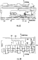
- FIGS. 2A and 2B illustrate example schematics 200a and 200b of the RFID printer 100, according to one or more embodiments described herein.
- the schematics 200a and 200b of the RFID printer 100 illustrate that the RFID printer 100 may further include a platen roller 202, a media sensor 204, a media guide 250, one or more shields 255, and a control system 206 in some embodiments.
- the schematics 200a and 200b of the RFID printer 100 further depicts the media path 122.
- the schematics 200a and 200b illustrate that the RFID antenna 104 is positioned adjacent to the media path 122 such that the RFID antenna 104 is pointed towards the media 116 on the media path 122. Further, in some examples, the RFID antenna 104 is positioned upstream of the media sensor 204.
- the term "upstream” according to the one or more embodiments described herein corresponds to a direction opposite to media traversal direction along the media path 122 during encoding of the RFID inlay 126 on the labels 118.
- the term “downstream” according to the one or more embodiments described herein corresponds to a direction same as the media traversal direction along the media path 122 during encoding of the RFID inlay 126 on the labels 118.
- FIG. 2C shows an example top view of an example media guide 250 and FIG. 2D shows an example bottom view of an example media guide 250.
- the RFID antenna 104 is coupled or otherwise attached to the media guide 250, such as via a slot 252 defined by the media guide 250, and communicatively coupled to the RFID control system 105 (e.g., via a coaxial cable 270).
- the RFID antenna 104 may include a grounding element 272 and one or more resistors 275.
- an antenna connection is made from a center pin of the coaxial cable 270 to the antenna 104 through the grounding element 272.
- the energy is then sent through the length of the coaxial cable 270 and moves through the opposite center pin, through a center antenna connection located on or within the grounding element 272 and is then radiated out from the antenna 104 in the form of RF signals toward an RFID inlay in range.
- the media guide 250 defines a plane that may be coupled or otherwise attached to the housing of the printer 100.
- An example shape of the plane defined by the media guide 250 is shown in FIGS. 2C and 2D .
- the media guide may attach to (at side 254) and extend outward from a wall of the housing of the printer 100.
- the media guide may be configured to be detachable and removable from the housing of the printer 100.
- the media guide is adjacent to the media path 122, as shown in FIG. 2A and 2B , in order to maintain the media path and prevent the media from skewing from the media path.
- the RFID antenna 104 may be coupled or otherwise attached to a top portion of the media guide 250 (e.g., via slot 252), such that the RFID antenna 104 rests on top of the media guide 250, as shown in FIG. 2C , while the media traverses underneath the bottom portion of the media guide, as shown in FIG. 2D .
- the media guide 250 is comprised of plastic or other nonmetallic material such that the media guide 250 does not interfere with signals (e.g., RF and/or other electromagnetic signals) transmitted from the RFID antenna 104 to one or more RFID inlays during an encoding process.
- the media guide 250 may be transparent such that light may pass through the media guide.
- one or more shields 255 may be coupled, fastened and/or otherwise attached to the media guide.
- the one or more shields 255 may be attached to the media guide in various ways.
- the shields 255 may clip and/or snap on to the media guide, and/or stick to the media guide (e.g., to the top or bottom of the media guide, via an adhesive).
- the shields 255 may be inserted into the media guide.
- the media guide may define one or more openings configured to receive the one or more shields 255.
- the one or more shields 255 may be configured to be removable from the media guide and positioned elsewhere on the media guide.
- the shields 255 may be positioned on the media guide based on the pitch of the labels of the media 116.
- the shields 255 may be positioned closer to the RFID antenna (e.g., as shown in FIG. 2A and 2B ).
- the one or more shields 255 are comprised of a metallic material capable of absorbing RF and/or other electromagnetic signals transmitted by the RFID antenna 104.
- the shields are comprised of copper.
- the shields are square or rectangularly shaped, though it is to be appreciated that the shields may be shaped in various ways.
- the shields may comprise a thickness of 0.5 millimeters. It is to be appreciated that the thickness of the shields may vary in some embodiments. For example, a thickness of the shields may be less than or greater than 0.5 millimeters.
- the one or more shields 255 comprise a length greater than or equal to a length of the antenna 104.
- the one or more shields 255 comprise a width at least equal to a width of the media 116.
- the one or more shields 255 may comprise a width at least equal to a maximum media width supported by the printer 100, such that the entirety of a label of the media upstream and/or downstream from the RFID antenna 104 is shielded during an encoding process.
- two shields 255 may be attached to the media guide 250, as shown in FIG. 2B , and positioned on the media guide 250 upstream and downstream from the RFID antenna 104 such that a first RFID inlay 261 of a first label 260 downstream from the RFID antenna 104 having already undergone an encoding process by the RFID antenna 104 and a second RFID inlay 264 of a second label 265 upstream from the RFID antenna are prevented from being detected and/or encoded by the RFID antenna 104 while a third RFID inlay 262 of a third label 263 currently below the RFID antenna 104 is undergoing an encoding process as the media 116 traverses the media path 122.
- the shields 255 are positioned such that the shields 255 absorb RF and/or other electromagnetic signals emitted by the RFID antenna 104 that would otherwise encode one or more additional RFID inlays 261 and 264, while still allowing the RFID inlay 262 below the RFID antenna 104 to be encoded.
- the shields 255 diminish the RF field directly below the shields 255 such that the RFID labels are not detected and/or encoded until the RFID inlay traverses into the RF field directly below the RFID antenna 104.
- a shield may be attached to the media guide 250 upstream from the RFID antenna at position 288 and a second shield may be attached to the media guide 250 downstream from the RFID antenna 104 at position 286.
- a single shield may be attached to the media guide 250 and positioned on the media guide 250 upstream and downstream from the RFID antenna 104 such that a first RFID inlay 261 of a first label 260 downstream from the RFID antenna 104 having already undergone an encoding process by the RFID antenna 104 and a second RFID inlay 264 of a second label 265 upstream from the RFID antenna are prevented from being detected and/or encoded by the RFID antenna 104 while a third RFID inlay 262 of a third label 263 currently below the RFID antenna 104 is undergoing an encoding process as the media 116 traverses the media path 122.
- the single shield may comprise an opening in the middle that allows transmission of RF and/or electromagnetic signals from the RFID antenna 104 to pass through.
- the platen roller 202 is positioned downstream of the print head 112 along the media path 122. As discussed above, the platen roller 202 is coupled to the first electrical drive that enables the platen roller 202 to rotate and pull the media 116 from the media roll 114, and accordingly cause the media 116 to travel along the media path 122.
- the media sensor 204 may correspond to a sensor that is configured to detect a presence of the media 116 on the media path 122.
- the media sensor 204 is positioned upstream of the print head 112 and downstream of the RFID antenna 104.
- the media sensor 204 may be configured to detect the presence of the media 116 by determining transmissivity and/or reflectivity of the media 116.
- the transmissivity of the media 116 may correspond to a measure of an intensity of a light signal that the media 116 allows to pass through it.
- the reflectivity of the media 116 may correspond to a measure of an intensity of light signal that gets reflected from a surface of the media 116.
- the media sensor 204 includes a light transmitter 210 and a light receiver 212.
- the light transmitter 210 may correspond to a light source, such as a Light Emitting Diode (LED), a LASER, and/or the like.
- the light transmitter 210 may be configured to direct the light signal on the media path 122.
- the light receiver 212 may correspond to at least one of a photodetector, a photodiode, or a photo resistor.
- the light receiver 212 may generate an input signal based on an intensity of the light signal received by the light receiver 212.
- the input signal may correspond to a voltage signal, where one or more characteristics of the voltage signal, such as the amplitude of the voltage signal and frequency of the voltage signal, are directly proportional to the intensity of the portion of the light signal received by the light receiver 212.
- the light transmitter 210 of the media sensor 204 may be configured to direct the light signal on the media path 122. If the media 116 is present on the media path 122, a portion of light signal may get reflected from the surface of the media 116.
- the light receiver 212 may receive the portion of the light signal, and based on the intensity of the portion of the received light signal, the light receiver 212 generates the input signal. In some implementations, where the media 116 is not present on the media path 122, the light receiver 212 may not receive the portion of the light signal (transmitted by the light transmitter), and therefore may not generate the input signal. Accordingly, based on the input signal generated by the media sensor 204, the presence of the media 116 on the media path 122 may be determined.
- the media sensor 204 may determine the presence of the media 116 on the media path 122 based on the transmissivity of the media 116.
- the light receiver 212 may receive the portion of the light signal that passes through the media 116. To receive the portion of the light signal that passes through the media 116, the light receiver 212 is spaced apart from the light transmitter 210 in such a manner that the media of media roll 114 passes through a space between the light receiver 212 and the light transmitter 210.
- the light transmitter 210 directs the light signal on the media 116
- the portion of the light signal passes through the media 116, which is then received by the light receiver 212.
- the light receiver 212 thereafter, may generate the input signal in accordance with the intensity of the portion of light signal received.
- the media sensor 204 may be utilized to detect a start portion and an end portion of the label 118a of the plurality of labels 118 in the media 116.
- the start portion of the label 118a may correspond to a first perforation between the label 118a and another label preceding the label 118a.
- the end portion of the label 118a may correspond to a second perforation between the label 118a and a yet another label succeeding the label 118a.
- the media 116 may include the plurality of labels 118 that are separated either by perforations 120 or by the one or more marks (not shown).
- the media sensor 204 may detect a sudden increase/decrease in the measure of transmissivity/reflectivity of media 116.
- Such sudden increase/decrease in the measure of the transmissivity/reflectivity of media 116 is reflected in the input signal generated by the media sensor 204.
- the input signal generated by the media sensor 204 may include peaks or valleys indicating a sudden increase or decrease in the measure of the transmissivity/reflectivity of media 116. Such peaks and valleys may be utilized to determine the start portion or the end portion of the label of the plurality of labels 118.
- the RFID control system 105 is communicatively coupled to the RFID antenna 104 and the control system 206.
- the control system 206 may include suitable logic and circuitry to control the operation of the RFID printer 100.
- the control system 206 may be communicatively coupled to one or more components of the RFID printer 100.
- the control system 206 may be communicatively coupled to the print head 112, the media sensor 204, the RFID control system 105, the first electrical drive (associated with the media hub 102 and the platen roller 202), the third electrical drive (coupled to the ribbon drive assembly 108 and the ribbon take-up hub 110), and the second electrical drive (coupled to the RFID antenna 104).
- the structure of the control system 206 is further described in conjunction with FIG. 4 .
- the scope of the disclosure is not limited to the RFID printer 100 that performs both the RFID inlay encoding and printing operations.
- the RFID printer 100 may not perform the printing operation and may only perform the RFID inlay encoding operation.
- the RFID printer 100 may not include the print head 112, the ribbon drive assembly 108, and the ribbon take-up hub 110.
- FIG. 3 illustrates a block diagram of the RFID control system 105, according to one or more embodiments described herein.
- the RFID control system 105 includes a controller 302, a first memory device 304, a first communication interface 306, an RFID encoder 308, an RFID reader 310, a verification unit 312, and a power modification unit 314.
- the controller 302 may be embodied as means including one or more microprocessors with accompanying digital signal processor(s), one or more processor(s) without an accompanying digital signal processor, one or more coprocessors, one or more multi-core processors, one or more controllers, processing circuitry, one or more computers, various other processing elements including integrated circuits such as, for example, an application specific integrated circuit (ASIC) or field programmable gate array (FPGA), or some combination thereof. Accordingly, although illustrated in FIG. 3 as a single controller, in an embodiment, the controller 302 may include a plurality of controllers and signal processing modules.
- ASIC application specific integrated circuit
- FPGA field programmable gate array
- the plurality of controllers may be embodied on a single electronic device or may be distributed across a plurality of electronic devices collectively configured to function as the circuitry of the RFID control system 105.
- the plurality of controllers may be in operative communication with each other and may be collectively configured to perform one or more functionalities of the circuitry of the RFID control system 105, as described herein.
- the controller 302 may be configured to execute instructions stored in the first memory device 304 or otherwise accessible to the controller 302. These instructions, when executed by the controller 302, may cause the circuitry of the RFID control system 105 to perform one or more of the functionalities, as described herein.
- the controller 302 may include an entity capable of performing operations according to embodiments of the present disclosure while configured accordingly.
- the controller 302 when the controller 302 is embodied as an ASIC, FPGA or the like, the controller 302 may include specifically configured hardware for conducting one or more operations described herein.
- the controller 302 when the controller 302 is embodied as an executor of instructions, such as may be stored in the first memory device 304, the instructions may specifically configure the controller 302 to perform one or more algorithms and operations described herein.
- the controller 302 used herein may refer to a programmable microprocessor, microcomputer or multiple processor chip or chips that can be configured by software instructions (applications) to perform a variety of functions, including the functions of the various embodiments described above.
- multiple processors may be provided dedicated to wireless communication functions and one processor dedicated to running other applications.
- Software applications may be stored in the internal memory before they are accessed and loaded into the processors.
- the processors may include internal memory sufficient to store the application software instructions.
- the internal memory may be a volatile or nonvolatile memory, such as flash memory, or a mixture of both.
- the memory can also be located internal to another computing resource (e.g., enabling computer readable instructions to be downloaded over the Internet or another wired or wireless connection).
- the first memory device 304 may include suitable logic, circuitry, and/or interfaces that are adapted to store a set of instructions that is executable by the controller 302 to perform predetermined operations.
- Some of the commonly known memory implementations include, but are not limited to, a hard disk, random access memory, cache memory, read only memory (ROM), erasable programmable read-only memory (EPROM) & electrically erasable programmable read-only memory (EEPROM), flash memory, magnetic cassettes, magnetic tape, magnetic disk storage or other magnetic storage devices, a compact disc read only memory (CD-ROM), digital versatile disc read only memory (DVD-ROM), an optical disc, circuitry configured to store information, or some combination thereof.
- the first memory device 304 may be integrated with the controller 302 on a single chip, without departing from the scope of the disclosure.
- the first communication interface 306 may correspond to a communication interface that may facilitate transmission and reception of messages and data to and from various components of the RFID printer 100.
- the first communication interface 306 is communicatively coupled with the control system 206.
- Examples of the communication interface may include, but are not limited to, an antenna, an Ethernet port, a USB port, a serial port, or any other port that can be adapted to receive and transmit data.
- the communication interface transmits and receives data and/or messages in accordance with the various communication protocols, such as, I2C, TCP/IP, UDP, and 2G, 3G, 4G or 5G communication protocols.
- the RFID encoder 308 includes suitable logic, and circuitry for encoding data in the RFID inlay 126 included in the plurality of labels 118 in the media.
- the RFID encoder 308 encodes data in the RFID inlay 126, according to one or more of Electronic Product code (EPC) or Department of Defense (DOD) formats.
- the RFID encoder 308 may be configured to transmit the data (for the purpose of encoding the RFID inlay 126) over one or more frequency bands such as, but not limited to, 13.56 MHz (hereinafter "High Frequency band” or "HF”) or 860 MHz-960 MHz (hereinafter "UHF band”), through the antenna element 316.
- HF 13.56 MHz
- UHF band 860 MHz-960 MHz
- the RFID encoder 308 may be configured to modulate the data on an RF carrier of either HF frequency band or UHF band prior to transmitting the data for encoding the RFID inlay 126.
- modulation techniques utilized by the RFID encoder 308 include, but are not limited to, Phase Jitter Modulation (PJM), Amplitude Shift Keying (ASK), and/or the like.
- the RFID encoder 308 may be configured to transmit one or more commands to the RFID inlay 126 on the label 118a of the plurality of the labels 118, causing the RFID inlay 126 to perform a predetermined operation in accordance with the one or more commands. For example, the RFID encoder 308 may transmit a command "Write” that indicates to the RFID inlay 126 to write the data accompanied with the command in the memory of the RFID inlay 126. Similarly, the RFID encoder 308 may transmit other commands to the RFID inlay 126 such as but not limited to "Lock”, “Access”, “BlockWrite”, and/or any other command according to the EPCglobal standards.
- the RFID reader 310 includes suitable logic and circuitry for reading data from the RFID inlay (e.g., 126). To read the data encoded in the RFID inlay 126, the RFID reader 310 may transmit an interrogation command to the RFID inlay over the one or more frequency bands such as HF and UHF. Further, similar to the RFID encoder 308, the RFID reader 310 may also utilize the one or more modulation techniques such as ASK and PJM to transmit the interrogation command on the one or more frequency bands. In response to the interrogation command, the RFID reader 310 may receive the encoded data from the RFID inlay 126. In an example embodiment, the RFID reader 310 may utilize the antenna element 316 to transmit the interrogation command and receive the encoded data from the RFID inlay 126.
- the RFID reader 310 may utilize the antenna element 316 to transmit the interrogation command and receive the encoded data from the RFID inlay 126.
- both the RFID reader 310 and the RFID encoder 308 may include one or more of filters, analog to digital (A/D) converters, Digital to Analog (D/A) convertors, matching circuits, amplifiers, and/or tuners that enable the RFID reader 310 and the RFID encoder 308 to transmit and receive data over the one or more frequency bands through the antenna element 316.
- filters analog to digital (A/D) converters, Digital to Analog (D/A) convertors, matching circuits, amplifiers, and/or tuners that enable the RFID reader 310 and the RFID encoder 308 to transmit and receive data over the one or more frequency bands through the antenna element 316.
- the verification unit 312 includes suitable logic and circuitry that is configured to verify whether the encoding of the RFID inlay 126 is successful, as further described in FIGS. 10 and 13. In some examples, to determine whether the encoding is successful, the verification unit 312 may determine an encode success rate.
- the verification unit 312 may be implemented using one or more hardware components, such as, but not limited to, FPGA, ASIC, and the like.
- the power modification unit 314 includes suitable logic and circuitry that is configured to manage a signal transmission power of the RFID antenna 104.
- the signal transmission power corresponds to a transmitter power output at which a signal is transmitted from the RFID antenna 104.
- the power modification unit 314 may be configured to modify the signal transmission power in accordance with a plurality of power settings.
- a power setting may correspond to a value of the signal transmission power with which the data is transmitted from the RFID antenna 104.
- the power modification unit 314 may modify input voltage to the RFID antenna 104 to modify the signal transmission power.
- the power modification unit 314 may modify the signal transmission power in response to an instruction received from the control system 206.
- the power modification unit 314 may be implemented using one or more hardware components, such as, but not limited to, FPGA, ASIC, and the like.
- FIG. 4 illustrates a block diagram of the control system 206 of the RFID printer 100, according to one or more embodiments described herein.
- the control system 206 includes a processor 402, a second memory device 404, a second communication interface 406, an input/output (I/O) device interface unit 408, a calibration unit 410, an encoding operation unit 412, and a signal processing unit 414.
- the processor 402 may be embodied as means including one or more microprocessors with accompanying digital signal processor(s), one or more processor(s) without an accompanying digital signal processor, one or more coprocessors, one or more multi-core processors, one or more controllers, processing circuitry, one or more computers, various other processing elements including integrated circuits such as, for example, an application specific integrated circuit (ASIC) or field programmable gate array (FPGA), or some combination thereof. Accordingly, although illustrated in FIG. 4 as a single processor, in an embodiment, the processor 402 may include a plurality of processors and signal processing modules.
- ASIC application specific integrated circuit
- FPGA field programmable gate array
- the plurality of processors may be embodied on a single electronic device or may be distributed across a plurality of electronic devices collectively configured to function as the circuitry of the control system 206.
- the plurality of processors may be in operative communication with each other and may be collectively configured to perform one or more functionalities of the circuitry of the control system 206, as described herein.
- the processor 402 may be configured to execute instructions stored in the second memory device 404 or otherwise accessible to the processor 402. These instructions, when executed by the processor 402, may cause the circuitry of the control system 206 to perform one or more of the functionalities, as described herein.
- the processor 402 may include an entity capable of performing operations according to embodiments of the present disclosure while configured accordingly.
- the processor 402 when the processor 402 is embodied as an ASIC, FPGA or the like, the processor 402 may include specifically configured hardware for conducting one or more operations described herein.
- the processor 402 when the processor 402 is embodied as an executor of instructions, such as may be stored in the second memory device 404, the instructions may specifically configure the processor 402 to perform one or more algorithms and operations described herein.
- the processor 402 used herein may refer to a programmable microprocessor, microcomputer or multiple processor chip or chips that can be configured by software instructions (applications) to perform a variety of functions, including the functions of the various embodiments described above.
- multiple processors may be provided dedicated to wireless communication functions and one processor dedicated to running other applications.
- Software applications may be stored in the internal memory before they are accessed and loaded into the processors.
- the processors may include internal memory sufficient to store the application software instructions.
- the internal memory may be a volatile or nonvolatile memory, such as flash memory, or a mixture of both.
- the memory can also be located internal to another computing resource (e.g., enabling computer readable instructions to be downloaded over the Internet or another wired or wireless connection).
- the second memory device 404 may include suitable logic, circuitry, and/or interfaces that are adapted to store a set of instructions that is executable by the processor 402 to perform predetermined operations.
- Some of the commonly known memory implementations include, but are not limited to, a hard disk, random access memory, cache memory, read only memory (ROM), erasable programmable read-only memory (EPROM) & electrically erasable programmable read-only memory (EEPROM), flash memory, magnetic cassettes, magnetic tape, magnetic disk storage or other magnetic storage devices, a compact disc read only memory (CD-ROM), digital versatile disc read only memory (DVD-ROM), an optical disc, circuitry configured to store information, or some combination thereof.
- the second memory device 404 may be integrated with the processor 402 on a single chip, without departing from the scope of the disclosure.
- the second communication interface 406 may correspond to a second communication interface 406 that may facilitate transmission and reception of messages and data to and from various devices.
- the second communication interface 406 is communicatively coupled with a computing device (not shown).
- the RFID printer 100 may be configured to receive commands/jobs from the computing device based on which the RFID printer 100 may perform predetermined operation.
- Examples of the second communication interface 406 may include, but are not limited to, an antenna, an Ethernet port, a USB port, a serial port, or any other port that can be adapted to receive and transmit data.
- the second communication interface 406 transmits and receives data and/or messages in accordance with the various communication protocols, such as, I2C, TCP/IP, UDP, and 2G, 3G, 4G or 5G communication protocols.
- the I/O device interface unit 408 may include suitable logic and/or circuitry that may be configured to communicate with the one or more components of the RFID printer 100, in accordance with one or more device communication protocols such as, but not limited to, I2C communication protocol, Serial Peripheral Interface (SPI) communication protocol, Serial communication protocol, Control Area Network (CAN) communication protocol, and 1-Wire ® communication protocol.
- the I/O device interface unit 408 may communicate with the media sensor 204, the first electrical drive, the second electrical drive, the third electrical drive, associated with the media hub 102, the RFID antenna 104, and the ribbon drive assembly 108 and the ribbon take-up hub 110, respectively, and the one or more buttons 136 provided the input panel 134 of the RFID printer 100.
- the I/O device interface unit 408 may receive the input signal from the media sensor 204. Further, for example, the I/O device interface unit 408 may actuate the first electrical drive associated with the media hub 102 and the platen roller 202 to cause the media 116 to traverse along the media path 122. Some examples of the I/O device interface unit 408 may include, but not limited to, a Data Acquisition (DAQ) card, an electrical drives driver circuit, and/or the like.
- DAQ Data Acquisition
- the encoding operation unit 412 may include suitable logic and/or circuitry for operating the RFID printer 100 in an encoding mode.
- the encoding operation unit 412 may be configured to cause the RFID encoder 308 in the RFID control system 105 to encode the RFID inlay 126 on the label 118a, through the RFID antenna 104.
- the encoding operation unit 412 may be implemented using one or more hardware components, such as, but not limited to, FPGA, ASIC, and the like.
- the signal processing unit 414 may include suitable logic and/or circuitry for analyzing the input signal received from the media sensor 204.
- the signal processing unit 414 may include a digital signal processor 402 that may be configured to identify the peaks and the valleys in the input signal.
- the signal processing unit 414 may utilize one or more signal processing techniques such as, but not limited to, Fast Fourier Transform (FFT), Discrete Fourier Transform (DFT), Discrete Time Fourier Transform (DTFT) to analyze the input signal.
- FFT Fast Fourier Transform
- DFT Discrete Fourier Transform
- DTFT Discrete Time Fourier Transform
- the signal processing unit 414 may be implemented using one or more hardware components, such as, but not limited to, FPGA, ASIC, and the like.
- the scope of the disclosure is not limited to having a separate control system 206 for the RFID printer 100.
- various units/modules of the control system 206 may be implemented on the RFID control system 105, forming an integrated, single apparatus, without departing from the scope of the disclosure.
- various functionalities of the RFID control system 105 may be implemented in the control system 206, forming an integrated, single apparatus, without departing from the scope of the disclosure.
- the RFID antenna 104 may be directly communicatively coupled to the control system 206.
- certain ones of the operations herein may be modified or further amplified as described below. Moreover, in some embodiments additional optional operations may also be included. It should be appreciated that each of the modifications, optional additions or amplifications described herein may be included with the operations herein either alone or in combination with any others among the features described herein.
- the hardware used to implement the various illustrative logics, logical blocks, modules, and circuits described in connection with the aspects disclosed herein may include a general purpose processor, a digital signal processor (DSP), a special-purpose processor such as an application specific integrated circuit (ASIC) or a field programmable gate array (FPGA), a programmable logic device, discrete gate or transistor logic, discrete hardware components, or any combination thereof designed to perform the functions described herein.
- a general-purpose processor may be a microprocessor, but, in the alternative, the processor 402 may be any processor, controller, or state machine.
- a processor 402 may also be implemented as a combination of computing devices, e.g., a combination of a DSP and a microprocessor, a plurality of microprocessors, one or more microprocessors in conjunction with a DSP core, or any other such configuration. Alternatively or in addition, some steps or methods may be performed by circuitry that is specific to a given function.
- the functions described herein may be implemented by special-purpose hardware or a combination of hardware programmed by firmware or other software. In implementations relying on firmware or other software, the functions may be performed as a result of execution of one or more instructions stored on one or more non-transitory computer-readable media and/or one or more non-transitory processor 402-readable media. These instructions may be embodied by one or more processor 402-executable software modules that reside on the one or more non-transitory computer-readable or processor 402-readable storage media.
- Non-transitory computer-readable or processor 402-readable storage media may in this regard comprise any storage media that may be accessed by a computer or a processor 402.
- non-transitory computer-readable or processor 402-readable media may include RAM, ROM, EEPROM, FLASH memory, disk storage, magnetic storage devices, or the like.
- Disk storage includes compact disc (CD), laser disc, optical disc, digital versatile disc (DVD), floppy disk, and Blu-ray disc TM , or other storage devices that store data magnetically or optically with lasers. Combinations of the above types of media are also included within the scope of the terms non-transitory computer-readable and processor 402-readable media. Additionally, any combination of instructions stored on the one or more non-transitory processor 402-readable or computer-readable media may be referred to herein as a computer program product.
Landscapes
- Engineering & Computer Science (AREA)
- Physics & Mathematics (AREA)
- General Physics & Mathematics (AREA)
- Theoretical Computer Science (AREA)
- Computer Hardware Design (AREA)
- Computer Networks & Wireless Communication (AREA)
- Microelectronics & Electronic Packaging (AREA)
- Electromagnetism (AREA)
- General Engineering & Computer Science (AREA)
- Toxicology (AREA)
- Health & Medical Sciences (AREA)
- Computer Security & Cryptography (AREA)
- Artificial Intelligence (AREA)
- Computer Vision & Pattern Recognition (AREA)
- General Health & Medical Sciences (AREA)
- Accessory Devices And Overall Control Thereof (AREA)
- Printers Characterized By Their Purpose (AREA)
Applications Claiming Priority (1)
| Application Number | Priority Date | Filing Date | Title |
|---|---|---|---|
| US17/188,149 US20220277184A1 (en) | 2021-03-01 | 2021-03-01 | Small pitch radio frequency identification (rfid) label detection |
Publications (3)
| Publication Number | Publication Date |
|---|---|
| EP4053741A2 true EP4053741A2 (fr) | 2022-09-07 |
| EP4053741A3 EP4053741A3 (fr) | 2022-09-28 |
| EP4053741B1 EP4053741B1 (fr) | 2024-10-16 |
Family
ID=80623907
Family Applications (1)
| Application Number | Title | Priority Date | Filing Date |
|---|---|---|---|
| EP22159082.1A Active EP4053741B1 (fr) | 2021-03-01 | 2022-02-28 | Ensemble imprimante avec détection d'étiquettes d'identification par radiofréquence (rfid) à petit pas |
Country Status (3)
| Country | Link |
|---|---|
| US (1) | US20220277184A1 (fr) |
| EP (1) | EP4053741B1 (fr) |
| CN (1) | CN114997194B (fr) |
Families Citing this family (3)
| Publication number | Priority date | Publication date | Assignee | Title |
|---|---|---|---|---|
| CN217279580U (zh) | 2021-11-22 | 2022-08-23 | 手持产品公司 | 具有可旋转天线支架部件的射频识别打印机 |
| FI131482B1 (en) * | 2023-08-02 | 2025-05-12 | Voyantic Oy | Indication of process status of a radio frequency tag |
| CN117081628B (zh) * | 2023-08-31 | 2024-11-15 | 厦门汉印股份有限公司 | 一种频点确定方法、装置、打印设备和存储介质 |
Family Cites Families (6)
| Publication number | Priority date | Publication date | Assignee | Title |
|---|---|---|---|---|
| US6104291A (en) * | 1998-01-09 | 2000-08-15 | Intermec Ip Corp. | Method and apparatus for testing RFID tags |
| CA2576772A1 (fr) * | 2004-08-17 | 2006-03-02 | Symbol Technologies, Inc. | Singulation d'etiquettes d'identification rf (rfid) pour l'essai et/ou la programmation |
| US8878652B2 (en) * | 2009-11-13 | 2014-11-04 | Zih Corp. | Encoding module, associated encoding element, connector, printer-encoder and access control system |
| US9211744B2 (en) * | 2013-12-16 | 2015-12-15 | Zih Corp. | Media processing device with enhanced media and ribbon loading and unloading features |
| US10628723B2 (en) * | 2018-07-10 | 2020-04-21 | Datamax-O'neil Corporation | Methods, systems, and apparatuses for encoding a radio frequency identification (RFID) inlay |
| JP7500306B2 (ja) * | 2020-07-01 | 2024-06-17 | 東芝テック株式会社 | Rfidタグ通信装置 |
-
2021
- 2021-03-01 US US17/188,149 patent/US20220277184A1/en not_active Abandoned
-
2022
- 2022-02-28 EP EP22159082.1A patent/EP4053741B1/fr active Active
- 2022-03-01 CN CN202210198109.5A patent/CN114997194B/zh active Active
Also Published As
| Publication number | Publication date |
|---|---|
| EP4053741B1 (fr) | 2024-10-16 |
| CN114997194B (zh) | 2025-11-11 |
| EP4053741A3 (fr) | 2022-09-28 |
| US20220277184A1 (en) | 2022-09-01 |
| CN114997194A (zh) | 2022-09-02 |
Similar Documents
| Publication | Publication Date | Title |
|---|---|---|
| EP4053741B1 (fr) | Ensemble imprimante avec détection d'étiquettes d'identification par radiofréquence (rfid) à petit pas | |
| US10956800B2 (en) | Methods, systems, and apparatuses for encoding a radio frequency identification (RFID) inlay | |
| US11949827B2 (en) | Methods, apparatus, and systems for improving printing precision | |
| US9147137B2 (en) | Label printer, and method of searching optimal communication position | |
| US8981910B2 (en) | RFID tag issuing apparatus and RFID tag misalignment detecting method | |
| US9962976B2 (en) | Methods and apparatus to detect an ink ribbon based on types of light | |
| US12387062B2 (en) | Systems and methods for encoding and decoding data | |
| JP2012131165A (ja) | サーマルプリンタ、サーマルプリンタのラベル用紙検出方法 | |
| EP3950362B1 (fr) | Imprimante, procédé de commande d'imprimante et programme | |
| US12265866B2 (en) | Methods and systems for encoding radio frequency identification (RFID) labels | |
| US20240092090A1 (en) | Printer device | |
| US10569574B2 (en) | Method and system for enhancing throughput of thermal printer cutter | |
| US20150036165A1 (en) | Media Processing Device, Media Processing System, and Control Method of a Media Processing Device | |
| JP2006306566A (ja) | シート状媒体搬送装置 |
Legal Events
| Date | Code | Title | Description |
|---|---|---|---|
| PUAI | Public reference made under article 153(3) epc to a published international application that has entered the european phase |
Free format text: ORIGINAL CODE: 0009012 |
|
| STAA | Information on the status of an ep patent application or granted ep patent |
Free format text: STATUS: REQUEST FOR EXAMINATION WAS MADE |
|
| PUAL | Search report despatched |
Free format text: ORIGINAL CODE: 0009013 |
|
| 17P | Request for examination filed |
Effective date: 20220228 |
|
| AK | Designated contracting states |
Kind code of ref document: A2 Designated state(s): AL AT BE BG CH CY CZ DE DK EE ES FI FR GB GR HR HU IE IS IT LI LT LU LV MC MK MT NL NO PL PT RO RS SE SI SK SM TR |
|
| AK | Designated contracting states |
Kind code of ref document: A3 Designated state(s): AL AT BE BG CH CY CZ DE DK EE ES FI FR GB GR HR HU IE IS IT LI LT LU LV MC MK MT NL NO PL PT RO RS SE SI SK SM TR |
|
| RIC1 | Information provided on ipc code assigned before grant |
Ipc: B65C 9/00 20060101ALI20220822BHEP Ipc: B41J 3/50 20060101ALI20220822BHEP Ipc: G06K 17/00 20060101AFI20220822BHEP |
|
| RIN1 | Information on inventor provided before grant (corrected) |
Inventor name: LEE, CHIN WEE Inventor name: RAMLI, RIZAM BIN Inventor name: CHIAP, CHENG YONG Inventor name: HAO, ZHENG |
|
| RIC1 | Information provided on ipc code assigned before grant |
Ipc: B65C 9/00 20060101ALN20240328BHEP Ipc: B41J 3/407 20060101ALN20240328BHEP Ipc: B65C 11/02 20060101ALI20240328BHEP Ipc: B41J 3/50 20060101ALI20240328BHEP Ipc: G06K 17/00 20060101AFI20240328BHEP |
|
| RIC1 | Information provided on ipc code assigned before grant |
Ipc: B65C 9/00 20060101ALN20240412BHEP Ipc: B41J 3/407 20060101ALN20240412BHEP Ipc: B65C 11/02 20060101ALI20240412BHEP Ipc: B41J 3/50 20060101ALI20240412BHEP Ipc: G06K 17/00 20060101AFI20240412BHEP |
|
| GRAP | Despatch of communication of intention to grant a patent |
Free format text: ORIGINAL CODE: EPIDOSNIGR1 |
|
| STAA | Information on the status of an ep patent application or granted ep patent |
Free format text: STATUS: GRANT OF PATENT IS INTENDED |
|
| INTG | Intention to grant announced |
Effective date: 20240607 |
|
| GRAS | Grant fee paid |
Free format text: ORIGINAL CODE: EPIDOSNIGR3 |
|
| GRAA | (expected) grant |
Free format text: ORIGINAL CODE: 0009210 |
|
| STAA | Information on the status of an ep patent application or granted ep patent |
Free format text: STATUS: THE PATENT HAS BEEN GRANTED |
|
| AK | Designated contracting states |
Kind code of ref document: B1 Designated state(s): AL AT BE BG CH CY CZ DE DK EE ES FI FR GB GR HR HU IE IS IT LI LT LU LV MC MK MT NL NO PL PT RO RS SE SI SK SM TR |
|
| REG | Reference to a national code |
Ref country code: GB Ref legal event code: FG4D |
|
| REG | Reference to a national code |
Ref country code: CH Ref legal event code: EP |
|
| REG | Reference to a national code |
Ref country code: IE Ref legal event code: FG4D |
|
| REG | Reference to a national code |
Ref country code: DE Ref legal event code: R096 Ref document number: 602022006762 Country of ref document: DE |
|
| REG | Reference to a national code |
Ref country code: DE Ref legal event code: R081 Ref document number: 602022006762 Country of ref document: DE Owner name: HAND HELD PRODUCTS, INC., CHARLOTTE, US Free format text: FORMER OWNER: HAND HELD PRODUCTS, INC., FORT MILL, SC, US |
|
| RAP4 | Party data changed (patent owner data changed or rights of a patent transferred) |
Owner name: HAND HELD PRODUCTS, INC. |
|
| REG | Reference to a national code |
Ref country code: LT Ref legal event code: MG9D |
|
| REG | Reference to a national code |
Ref country code: NL Ref legal event code: MP Effective date: 20241016 |
|
| REG | Reference to a national code |
Ref country code: AT Ref legal event code: MK05 Ref document number: 1733512 Country of ref document: AT Kind code of ref document: T Effective date: 20241016 |
|
| PG25 | Lapsed in a contracting state [announced via postgrant information from national office to epo] |
Ref country code: NL Free format text: LAPSE BECAUSE OF FAILURE TO SUBMIT A TRANSLATION OF THE DESCRIPTION OR TO PAY THE FEE WITHIN THE PRESCRIBED TIME-LIMIT Effective date: 20241016 |
|
| PG25 | Lapsed in a contracting state [announced via postgrant information from national office to epo] |
Ref country code: NL Free format text: LAPSE BECAUSE OF FAILURE TO SUBMIT A TRANSLATION OF THE DESCRIPTION OR TO PAY THE FEE WITHIN THE PRESCRIBED TIME-LIMIT Effective date: 20241016 |
|
| PG25 | Lapsed in a contracting state [announced via postgrant information from national office to epo] |
Ref country code: IS Free format text: LAPSE BECAUSE OF FAILURE TO SUBMIT A TRANSLATION OF THE DESCRIPTION OR TO PAY THE FEE WITHIN THE PRESCRIBED TIME-LIMIT Effective date: 20250216 Ref country code: HR Free format text: LAPSE BECAUSE OF FAILURE TO SUBMIT A TRANSLATION OF THE DESCRIPTION OR TO PAY THE FEE WITHIN THE PRESCRIBED TIME-LIMIT Effective date: 20241016 Ref country code: PT Free format text: LAPSE BECAUSE OF FAILURE TO SUBMIT A TRANSLATION OF THE DESCRIPTION OR TO PAY THE FEE WITHIN THE PRESCRIBED TIME-LIMIT Effective date: 20250217 |
|
| PG25 | Lapsed in a contracting state [announced via postgrant information from national office to epo] |
Ref country code: FI Free format text: LAPSE BECAUSE OF FAILURE TO SUBMIT A TRANSLATION OF THE DESCRIPTION OR TO PAY THE FEE WITHIN THE PRESCRIBED TIME-LIMIT Effective date: 20241016 |
|
| PG25 | Lapsed in a contracting state [announced via postgrant information from national office to epo] |
Ref country code: BG Free format text: LAPSE BECAUSE OF FAILURE TO SUBMIT A TRANSLATION OF THE DESCRIPTION OR TO PAY THE FEE WITHIN THE PRESCRIBED TIME-LIMIT Effective date: 20241016 |
|
| PG25 | Lapsed in a contracting state [announced via postgrant information from national office to epo] |
Ref country code: ES Free format text: LAPSE BECAUSE OF FAILURE TO SUBMIT A TRANSLATION OF THE DESCRIPTION OR TO PAY THE FEE WITHIN THE PRESCRIBED TIME-LIMIT Effective date: 20241016 |
|
| PG25 | Lapsed in a contracting state [announced via postgrant information from national office to epo] |
Ref country code: NO Free format text: LAPSE BECAUSE OF FAILURE TO SUBMIT A TRANSLATION OF THE DESCRIPTION OR TO PAY THE FEE WITHIN THE PRESCRIBED TIME-LIMIT Effective date: 20250116 |
|
| PG25 | Lapsed in a contracting state [announced via postgrant information from national office to epo] |
Ref country code: GR Free format text: LAPSE BECAUSE OF FAILURE TO SUBMIT A TRANSLATION OF THE DESCRIPTION OR TO PAY THE FEE WITHIN THE PRESCRIBED TIME-LIMIT Effective date: 20250117 Ref country code: AT Free format text: LAPSE BECAUSE OF FAILURE TO SUBMIT A TRANSLATION OF THE DESCRIPTION OR TO PAY THE FEE WITHIN THE PRESCRIBED TIME-LIMIT Effective date: 20241016 Ref country code: LV Free format text: LAPSE BECAUSE OF FAILURE TO SUBMIT A TRANSLATION OF THE DESCRIPTION OR TO PAY THE FEE WITHIN THE PRESCRIBED TIME-LIMIT Effective date: 20241016 |
|
| PG25 | Lapsed in a contracting state [announced via postgrant information from national office to epo] |
Ref country code: PL Free format text: LAPSE BECAUSE OF FAILURE TO SUBMIT A TRANSLATION OF THE DESCRIPTION OR TO PAY THE FEE WITHIN THE PRESCRIBED TIME-LIMIT Effective date: 20241016 |
|
| PG25 | Lapsed in a contracting state [announced via postgrant information from national office to epo] |
Ref country code: RS Free format text: LAPSE BECAUSE OF FAILURE TO SUBMIT A TRANSLATION OF THE DESCRIPTION OR TO PAY THE FEE WITHIN THE PRESCRIBED TIME-LIMIT Effective date: 20250116 |
|
| PG25 | Lapsed in a contracting state [announced via postgrant information from national office to epo] |
Ref country code: SM Free format text: LAPSE BECAUSE OF FAILURE TO SUBMIT A TRANSLATION OF THE DESCRIPTION OR TO PAY THE FEE WITHIN THE PRESCRIBED TIME-LIMIT Effective date: 20241016 |
|
| PG25 | Lapsed in a contracting state [announced via postgrant information from national office to epo] |
Ref country code: DK Free format text: LAPSE BECAUSE OF FAILURE TO SUBMIT A TRANSLATION OF THE DESCRIPTION OR TO PAY THE FEE WITHIN THE PRESCRIBED TIME-LIMIT Effective date: 20241016 |
|
| REG | Reference to a national code |
Ref country code: DE Ref legal event code: R097 Ref document number: 602022006762 Country of ref document: DE |
|
| PG25 | Lapsed in a contracting state [announced via postgrant information from national office to epo] |
Ref country code: EE Free format text: LAPSE BECAUSE OF FAILURE TO SUBMIT A TRANSLATION OF THE DESCRIPTION OR TO PAY THE FEE WITHIN THE PRESCRIBED TIME-LIMIT Effective date: 20241016 |
|
| PG25 | Lapsed in a contracting state [announced via postgrant information from national office to epo] |
Ref country code: RO Free format text: LAPSE BECAUSE OF FAILURE TO SUBMIT A TRANSLATION OF THE DESCRIPTION OR TO PAY THE FEE WITHIN THE PRESCRIBED TIME-LIMIT Effective date: 20241016 |
|
| PG25 | Lapsed in a contracting state [announced via postgrant information from national office to epo] |
Ref country code: SK Free format text: LAPSE BECAUSE OF FAILURE TO SUBMIT A TRANSLATION OF THE DESCRIPTION OR TO PAY THE FEE WITHIN THE PRESCRIBED TIME-LIMIT Effective date: 20241016 |
|
| PG25 | Lapsed in a contracting state [announced via postgrant information from national office to epo] |
Ref country code: CZ Free format text: LAPSE BECAUSE OF FAILURE TO SUBMIT A TRANSLATION OF THE DESCRIPTION OR TO PAY THE FEE WITHIN THE PRESCRIBED TIME-LIMIT Effective date: 20241016 |
|
| PG25 | Lapsed in a contracting state [announced via postgrant information from national office to epo] |
Ref country code: IT Free format text: LAPSE BECAUSE OF FAILURE TO SUBMIT A TRANSLATION OF THE DESCRIPTION OR TO PAY THE FEE WITHIN THE PRESCRIBED TIME-LIMIT Effective date: 20241016 |
|
| PLBE | No opposition filed within time limit |
Free format text: ORIGINAL CODE: 0009261 |
|
| STAA | Information on the status of an ep patent application or granted ep patent |
Free format text: STATUS: NO OPPOSITION FILED WITHIN TIME LIMIT |
|
| PG25 | Lapsed in a contracting state [announced via postgrant information from national office to epo] |
Ref country code: SE Free format text: LAPSE BECAUSE OF FAILURE TO SUBMIT A TRANSLATION OF THE DESCRIPTION OR TO PAY THE FEE WITHIN THE PRESCRIBED TIME-LIMIT Effective date: 20241016 |
|
| PG25 | Lapsed in a contracting state [announced via postgrant information from national office to epo] |
Ref country code: MC Free format text: LAPSE BECAUSE OF FAILURE TO SUBMIT A TRANSLATION OF THE DESCRIPTION OR TO PAY THE FEE WITHIN THE PRESCRIBED TIME-LIMIT Effective date: 20241016 |
|
| 26N | No opposition filed |
Effective date: 20250717 |
|
| REG | Reference to a national code |
Ref country code: CH Ref legal event code: PL |
|
| PG25 | Lapsed in a contracting state [announced via postgrant information from national office to epo] |
Ref country code: LU Free format text: LAPSE BECAUSE OF NON-PAYMENT OF DUE FEES Effective date: 20250228 |
|
| PG25 | Lapsed in a contracting state [announced via postgrant information from national office to epo] |
Ref country code: CH Free format text: LAPSE BECAUSE OF NON-PAYMENT OF DUE FEES Effective date: 20250228 |
|
| REG | Reference to a national code |
Ref country code: BE Ref legal event code: MM Effective date: 20250228 |
|
| PG25 | Lapsed in a contracting state [announced via postgrant information from national office to epo] |
Ref country code: FR Free format text: LAPSE BECAUSE OF NON-PAYMENT OF DUE FEES Effective date: 20250228 |
|
| PG25 | Lapsed in a contracting state [announced via postgrant information from national office to epo] |
Ref country code: BE Free format text: LAPSE BECAUSE OF NON-PAYMENT OF DUE FEES Effective date: 20250228 |
|
| PG25 | Lapsed in a contracting state [announced via postgrant information from national office to epo] |
Ref country code: IE Free format text: LAPSE BECAUSE OF NON-PAYMENT OF DUE FEES Effective date: 20250228 |
|
| PGFP | Annual fee paid to national office [announced via postgrant information from national office to epo] |
Ref country code: GB Payment date: 20260223 Year of fee payment: 5 |
|
| PGFP | Annual fee paid to national office [announced via postgrant information from national office to epo] |
Ref country code: DE Payment date: 20260220 Year of fee payment: 5 |