EP4061100B1 - Connecteurs électriques pour dispositifs médicaux - Google Patents
Connecteurs électriques pour dispositifs médicaux Download PDFInfo
- Publication number
- EP4061100B1 EP4061100B1 EP22160738.5A EP22160738A EP4061100B1 EP 4061100 B1 EP4061100 B1 EP 4061100B1 EP 22160738 A EP22160738 A EP 22160738A EP 4061100 B1 EP4061100 B1 EP 4061100B1
- Authority
- EP
- European Patent Office
- Prior art keywords
- circuit board
- fingers
- flexible circuit
- main support
- walls
- Prior art date
- Legal status (The legal status is an assumption and is not a legal conclusion. Google has not performed a legal analysis and makes no representation as to the accuracy of the status listed.)
- Active
Links
Images




Classifications
-
- H—ELECTRICITY
- H05—ELECTRIC TECHNIQUES NOT OTHERWISE PROVIDED FOR
- H05K—PRINTED CIRCUITS; CASINGS OR CONSTRUCTIONAL DETAILS OF ELECTRIC APPARATUS; MANUFACTURE OF ASSEMBLAGES OF ELECTRICAL COMPONENTS
- H05K1/00—Printed circuits
- H05K1/02—Details
- H05K1/11—Printed elements for providing electric connections to or between printed circuits
- H05K1/118—Printed elements for providing electric connections to or between printed circuits specially for flexible printed circuits, e.g. using folded portions
-
- H—ELECTRICITY
- H01—ELECTRIC ELEMENTS
- H01R—ELECTRICALLY-CONDUCTIVE CONNECTIONS; STRUCTURAL ASSOCIATIONS OF A PLURALITY OF MUTUALLY-INSULATED ELECTRICAL CONNECTING ELEMENTS; COUPLING DEVICES; CURRENT COLLECTORS
- H01R13/00—Details of coupling devices of the kinds covered by groups H01R12/70 or H01R24/00 - H01R33/00
- H01R13/40—Securing contact members in or to a base or case; Insulating of contact members
- H01R13/42—Securing in a demountable manner
- H01R13/422—Securing in resilient one-piece base or case, e.g. by friction; One-piece base or case formed with resilient locking means
- H01R13/4223—Securing in resilient one-piece base or case, e.g. by friction; One-piece base or case formed with resilient locking means comprising integral flexible contact retaining fingers
-
- A—HUMAN NECESSITIES
- A61—MEDICAL OR VETERINARY SCIENCE; HYGIENE
- A61B—DIAGNOSIS; SURGERY; IDENTIFICATION
- A61B5/00—Measuring for diagnostic purposes; Identification of persons
- A61B5/24—Detecting, measuring or recording bioelectric or biomagnetic signals of the body or parts thereof
- A61B5/25—Bioelectric electrodes therefor
- A61B5/279—Bioelectric electrodes therefor specially adapted for particular uses
- A61B5/28—Bioelectric electrodes therefor specially adapted for particular uses for electrocardiography [ECG]
- A61B5/283—Invasive
-
- A—HUMAN NECESSITIES
- A61—MEDICAL OR VETERINARY SCIENCE; HYGIENE
- A61B—DIAGNOSIS; SURGERY; IDENTIFICATION
- A61B5/00—Measuring for diagnostic purposes; Identification of persons
- A61B5/24—Detecting, measuring or recording bioelectric or biomagnetic signals of the body or parts thereof
- A61B5/30—Input circuits therefor
- A61B5/301—Input circuits therefor providing electrical separation, e.g. by using isolating transformers or optocouplers
-
- A—HUMAN NECESSITIES
- A61—MEDICAL OR VETERINARY SCIENCE; HYGIENE
- A61B—DIAGNOSIS; SURGERY; IDENTIFICATION
- A61B5/00—Measuring for diagnostic purposes; Identification of persons
- A61B5/24—Detecting, measuring or recording bioelectric or biomagnetic signals of the body or parts thereof
- A61B5/30—Input circuits therefor
- A61B5/307—Input circuits therefor specially adapted for particular uses
- A61B5/308—Input circuits therefor specially adapted for particular uses for electrocardiography [ECG]
-
- H—ELECTRICITY
- H01—ELECTRIC ELEMENTS
- H01R—ELECTRICALLY-CONDUCTIVE CONNECTIONS; STRUCTURAL ASSOCIATIONS OF A PLURALITY OF MUTUALLY-INSULATED ELECTRICAL CONNECTING ELEMENTS; COUPLING DEVICES; CURRENT COLLECTORS
- H01R12/00—Structural associations of a plurality of mutually-insulated electrical connecting elements, specially adapted for printed circuits, e.g. printed circuit boards [PCB], flat or ribbon cables, or like generally planar structures, e.g. terminal strips, terminal blocks; Coupling devices specially adapted for printed circuits, flat or ribbon cables, or like generally planar structures; Terminals specially adapted for contact with, or insertion into, printed circuits, flat or ribbon cables, or like generally planar structures
- H01R12/70—Coupling devices
- H01R12/77—Coupling devices for flexible printed circuits, flat or ribbon cables or like structures
- H01R12/777—Coupling parts carrying pins, blades or analogous contacts
-
- H—ELECTRICITY
- H01—ELECTRIC ELEMENTS
- H01R—ELECTRICALLY-CONDUCTIVE CONNECTIONS; STRUCTURAL ASSOCIATIONS OF A PLURALITY OF MUTUALLY-INSULATED ELECTRICAL CONNECTING ELEMENTS; COUPLING DEVICES; CURRENT COLLECTORS
- H01R13/00—Details of coupling devices of the kinds covered by groups H01R12/70 or H01R24/00 - H01R33/00
- H01R13/66—Structural association with built-in electrical component
- H01R13/665—Structural association with built-in electrical component with built-in electronic circuit
- H01R13/6658—Structural association with built-in electrical component with built-in electronic circuit on printed circuit board
-
- H—ELECTRICITY
- H01—ELECTRIC ELEMENTS
- H01R—ELECTRICALLY-CONDUCTIVE CONNECTIONS; STRUCTURAL ASSOCIATIONS OF A PLURALITY OF MUTUALLY-INSULATED ELECTRICAL CONNECTING ELEMENTS; COUPLING DEVICES; CURRENT COLLECTORS
- H01R12/00—Structural associations of a plurality of mutually-insulated electrical connecting elements, specially adapted for printed circuits, e.g. printed circuit boards [PCB], flat or ribbon cables, or like generally planar structures, e.g. terminal strips, terminal blocks; Coupling devices specially adapted for printed circuits, flat or ribbon cables, or like generally planar structures; Terminals specially adapted for contact with, or insertion into, printed circuits, flat or ribbon cables, or like generally planar structures
- H01R12/70—Coupling devices
- H01R12/71—Coupling devices for rigid printing circuits or like structures
- H01R12/72—Coupling devices for rigid printing circuits or like structures coupling with the edge of the rigid printed circuits or like structures
- H01R12/721—Coupling devices for rigid printing circuits or like structures coupling with the edge of the rigid printed circuits or like structures cooperating directly with the edge of the rigid printed circuits
-
- H—ELECTRICITY
- H05—ELECTRIC TECHNIQUES NOT OTHERWISE PROVIDED FOR
- H05K—PRINTED CIRCUITS; CASINGS OR CONSTRUCTIONAL DETAILS OF ELECTRIC APPARATUS; MANUFACTURE OF ASSEMBLAGES OF ELECTRICAL COMPONENTS
- H05K2201/00—Indexing scheme relating to printed circuits covered by H05K1/00
- H05K2201/05—Flexible printed circuits [FPCs]
- H05K2201/056—Folded around rigid support or component
-
- H—ELECTRICITY
- H05—ELECTRIC TECHNIQUES NOT OTHERWISE PROVIDED FOR
- H05K—PRINTED CIRCUITS; CASINGS OR CONSTRUCTIONAL DETAILS OF ELECTRIC APPARATUS; MANUFACTURE OF ASSEMBLAGES OF ELECTRICAL COMPONENTS
- H05K2201/00—Indexing scheme relating to printed circuits covered by H05K1/00
- H05K2201/09—Shape and layout
- H05K2201/09009—Substrate related
- H05K2201/09063—Holes or slots in insulating substrate not used for electrical connections
Definitions
- the present disclosure generally relates to an electrical connector for a medical device, and to a method for making an electrical connector for a medical device.
- Medical devices in the field often include a host device providing a display of data and controls of the device, as well as a peripheral device that somehow engages with the patient to collect this data for display.
- the peripheral device in many cases is connected by a leadwire to the host device, and particularly by an electrical connector of the leadwire being receivable within an input port of the host device. This allows the peripheral device to be removable from the host device for ease of replacement due to damage, or to enable disposable peripheral devices and/or leadwires for convenience and/or sanitation purposes.
- Section 4.2.1 of AAMI EC53 standard refers to the DIN 42-802 standard for ECG leadwire connector requirements to mitigate the potential hazard of a patient connected leadwire inadvertently making electrical contact with the power mains or other hazardous voltage sources.
- the DIN 42-802 standard specifies that a standard test probe such as a finger not be able to make electrical contact with the ECG leadwire connector pins (or sockets) when applied with a force of 30 N (6.744 lbs.).
- Section 8.5.2.3 of the AAMI ES60601-1 2005 C1 2009 has similar requirement except the test probe force is reduced to 10 N (2.248 lbs.).
- Section 8.9.1.15 relates to creepage distances and air clearances for defibrillation-proof applied parts.
- IEC 60601-1 standard requires 1.0 mm (0.039 in.) creepage distance, 0.5 mm (0.0196 in.) of air clearance, and a dielectric strength of 1,500 Vac for at least 1 minute, protection from mains voltage.
- Defibrillation patient safety requirements of AAMI EC11:1991/(R)2001 dictate that the reduction in energy delivered to a patient being defibrillated be less than 10% of the total energy delivered by the defibrillator while an electrocardiograph and its associated leadwires are attached to the patient in order to maintain the efficacy of defibrillation.
- the defibrillator generates voltages of up to 5000V peak, therefore, in order to prevent "arcing" of defib energy shunting around the patient, the leadwires and the connector must maintain adequate electrical isolation (i.e., withstand 5000V peak). In order to guarantee this level of isolation a 8.0mm (0.314 in.) creepage distance, 4.0mm (0.157 in.) of air clearance must be maintained in order to support a dielectric breakdown strength of 5,000 volts between the exposed conductive surfaces of the connector. These dimensional requirements are based upon the assumptions of a pollution degree 2 level, using materials with a comparative tracking index (CTI) greater than 175 for the substrate, at an altitude less than 2000 meters above sea level. The non-exposed conductor areas of the connector/leadwire must also be constructed to support the 5,000 volt withstand level by incorporating appropriate conductor spacing's based upon the specific dielectric materials in between them.
- CTI comparative tracking index
- US 2011/0147062 A1 describes a feedthrough flat-through capacitor that includes a capacitor having a first and second set of electrode plates, a first feedthrough passageway through the capacitor, a first lead disposed within the first feedthrough passageway and conductively coupled to the first set of electrode plates, a second feedthrough passageway through the capacitor disposed remote from the first feedthrough passageway, and a second lead disposed within the second feedthrough passageway and conductively coupled to the first set of electrode plates.
- the second set of electrode plates are typically conductively coupled to a ground.
- An EMI shield may be provided to electromagnetically isolate the first lead from the second lead.
- US 5040997 A describes a flex circuit connector assembly which includes folding one end of a flex circuit having contact pads to form a male contact portion. The male contact portion is then inserted into a female socket of an edge connector for electrically interconnecting the contact pads of the flex circuit to mating contacts disposed in the female socket of the edge connector.
- the edge connector includes pins for mounting it to a receptacle of a wired circuit.
- One embodiment of the present disclosure generally relates to an electrical connector for a medical device according to claim 1.
- the front difference is different than the height difference.
- main support walls among the walls are coupled to the left and the right of the main support, the main support walls each having a top and a bottom opposite the top that define a main support wall height therebetween, where a main support height is defined between the top and the bottom of the main support, and where the main support wall height is greater than the main support height.
- the main support walls are coplanar with two of the walls, where the wall heights equal the main support wall heights.
- a lock opening is defined through the flexible circuit board, where the lock opening is closer than the board edge to the main section along the outer surface of the flexible circuit board.
- a lock protrusion extends away from the bottom of the main support, where when the flexible circuit board is wrapped around the fingers the lock protrusion of the main support is received within the lock opening defined in the flexible circuit board.
- the flexible circuit board has a main section and a moveable section that extends forwardly from the main section to a board edge, the main section being supported by the main support when the flexible circuit board is wrapped around fingers, where the openings defined through the flexible circuit board have a front boundary that is closer than the board edge to the main section along the outer surface of the flexible circuit board.
- the electrical leads extend from first to second ends, where the first ends are positioned on the fingers when the flexible circuit board is wrapped around the fingers.
- each of the electrical leads has an exposed contact between the first and second ends configured for electrically engaging with the medical device, and the exposed contacts are positioned on the tips of the fingers when the flexible circuit board is wrapped around the fingers.
- the flexible circuit board has a main section and a moveable section that extends forwardly from the main section to a board edge, the main section being supported by the main support when the flexible circuit board is wrapped around fingers, where the openings defined through the flexible circuit board have a front boundary that is closer than the board edge to the main section along the outer surface of the flexible circuit board, and where the front boundaries of the openings defined in the flexible circuit board are closer than the first ends of the electrical leads to the board edge.
- the fingers comprise at least five fingers that are coplanar with each other and with the main support.
- the flexible circuit board is a flexible printed circuit board having exposed contacts, and wherein the inner surface of the flexible printed circuit board is free of exposed contacts.
- the exposed contacts are all a same distance from the front of the main support along the outer surface when the flexible circuit board is wrapped around fingers.
- Another embodiment generally relates to a method for making an electrical connector for a medical device according to claim 12.
- the flexible circuit board has a main section and a moveable section that extends forwardly from the main section to a board edge.
- a lock opening is defined through the flexible circuit board to be closer than the board edge to the main section along the outer surface of the flexible circuit board.
- a lock protrusion extends away from the bottom of the main support, where when the flexible circuit board is wrapped around the fingers the lock protrusion of the main support is received within the lock opening defined in the flexible circuit board, where the electrical leads extend from first to second ends, where the first ends are positioned on the fingers when the flexible circuit board is wrapped around the fingers, where each of the electrical leads has an exposed contact between the first and second ends configured for electrically engaging with the medical device, and where the exposed contacts are positioned on the tips of the fingers when the flexible circuit board is wrapped around the fingers.
- Another embodiment generally relates to an electrical connector for a medical device, the connector having a main support with a front and a back opposite the front, a top and a bottom opposite the top, and a left and a right opposite the left, where a lock protrusion extends away from the bottom of the main support.
- Fingers extend forwardly from the front of the main support to a tip, where the fingers have a top and a bottom opposite the top, where a finger height is defined between the tops and bottoms of the fingers, where the fingers are arranged from the left to the right of the main support such that gaps are defined between the fingers, and where the fingers are coplanar with each other and with the main support.
- Walls sandwich each of the fingers, where the walls each have a top and a bottom opposite the top that define a wall height therebetween, where the walls extend away from the main support to a front edge, and where at least one of the wall height of each of the walls is greater than the finger height of each of the fingers and the front edges of the walls extends farther than the tips of the fingers from the main support, where the wall height of each of the walls is greater than the finger height of each of the fingers, and where the front edges of the walls extends farther than the tips of the fingers from the main support.
- a flexible circuit board has an outer surface and an inner surface opposite the outer surface, where the flexible circuit board has a main section and a moveable section that extends forwardly from the main section to a board edge, where the flexible circuit board includes electrical leads that are exposed on the outer surface thereof, where openings are defined through the flexible circuit board between the electrical leads, and where the flexible circuit board is wrapped around the fingers such that the outer surface of the flexible circuit board is supported on both the top and the bottom of the fingers and the openings in the flexible circuit board are aligned with the gaps between the fingers, where a lock opening is defined through the flexible circuit board, where the lock opening is closer than the board edge to the main section along the outer surface of the flexible circuit board, and where when the flexible circuit board is wrapped around the fingers the lock protrusion of the main support is received within the lock opening defined in the flexible circuit board.
- the present inventors have identified that electrical connectors presently known in the art, and particularly those for disposable peripheral devices including flexible printed circuit boards, are susceptible to water ingress and contamination. Due to the flat surfaces, the appropriate creepage and air clearances are difficult to achieve, thereby resulting in large and heavy electrical connectors. Likewise, the flatform factor limits the direction of the electrical contact points for meeting within the corresponding input ports, and the flat and wide connectors having open contact pads make them hard to protect against making contact with non-flat surfaces. Through experimentation and development, the inventors have developed the presently disclosed electrical connectors, which overcome the problems discussed above.
- FIG. 1 depicts an exemplary medical device 30 as generally known in the art, but now incorporating a system 1 according to the present disclosure.
- the medical device 30 includes a host device 32 having a display 34, controls 36, and input port 38, whereby the input port 38 provides a basis for connecting the host device 32 to a peripheral device 40.
- the peripheral device 40 is a disposable neuromuscular transmission device having three electrodes 29 configured for positioning on a patient, such as GE Healthcare's NMT Module Entropy Sensor.
- the electrodes 42 are coupled together by leadwires 44, which through the electrical connector 50 presently disclosed is receivable within the input port 38 of the host device 32 to provide communication between the host device 32 and peripheral device 40.
- Other exemplary peripheral devices 40 include GE Healthcare's MAC VU360 Resting ECG or CASE Exercise testing system, for example. Non-healthcare applications for the presently disclosed electrical connector 50 are also contemplated by the present disclosure, such as consumer electronics.
- FIG. 2 depicts a prior art connector 2 as presently known in the art.
- the front 4 of the prior art connector 2 is configured to be inserted in an input port similar to the input port 38 of FIG. 1 , but specifically configured to correspond to the prior art connector 2.
- the prior art connector 2 has a top 6 and opposite bottom 8 and is comprised of a rigid portion 10 with a flexible circuit board 20 positioned on top.
- a slot 12 is defined through the rigid portion 10 and extends rearwardly from the front 4, the slot 12 having a width 14 and length 16.
- the slot 12 is used in part to provide electrical isolation between two separate functions in the same applied part (e.g., transmitting signals or receiving signals), or between different functions.
- the slot 12 provides that patient stimulating current is separated from the sensor electromyograph (EMG) electrodes.
- EMG sensor electromyograph
- a large air clearance can be achieved when the electrical connector 50 is mated with the input port 38 of the host device 32.
- the creepage distance requirement can be greater that the required air clearance, especially if moisture/pollution is present inside the electrical connector 50.
- the slot 12 will separate two halves of the electrical connector 50 from each other so that the creepage distance is significantly greater.
- the slot 12 can and or alternatively function as a poke-yoke, ensuring that the electrical connector 50 is inserted into the input port 38 in the intended orientation.
- the flexible circuit board 20 has a front 22 substantially aligned with the front 4 of the prior art connector 2, which also has a slot 25 that substantially overlays the slot 12 of the rigid portion 10.
- the flexible circuit board 20 includes a plurality of leads 21 running through the flexible circuit board 20, which terminate at exposed contacts 23 near the front 22 of the flexible circuit board 20.
- distances D1, D2, and D3 are shown between the exposed contacts 23, particularly denoting the shortest distances between these exposed contacts 23.
- a slot 24 is also defined within the flexible circuit board 20, which in the present example is intended to increase separation between two of the exposed contacts 23 in view of the regulations regarding clearances.
- This prior art connector 2 is subject to the problems described above, including being susceptible to water ingress and contamination from the configuration of the exposed contacts. Likewise, the configuration is limited in terms of how many exposed contacts 23 may be positioned on the prior art connector 2 due to creepage and air clearance requirements, which are nonetheless separated by relatively small distances D1-D3. In the example shown, the exposed contacts 23 are a minimum of 2.0 mm apart from each other. The prior art connector 2 is also limited in that the exposed contacts 23 must be positioned on the top 6 of the prior art connector 2, limiting the manner in which these exposed contacts 23 may make contact with the host device via the corresponding input port. Moreover, as is apparent from the view of FIG. 2 , the inventors have recognized that it is hazardously simple to make electrical contact between exposed contacts 23 in this configuration, for example via accidental contact with conductive objects.
- the present inventors have developed an alternative electrical connector that mitigates against the electrical hazards presently known of flexible circuit board type connectors in the art.
- the presently disclosed connectors also advantageously provide a cost-effective design and a compact form factor while nonetheless fulfilling the safety requirements and considerations described above.
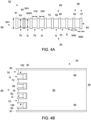
- FIGS. 3A-3B depict an exemplary rigid base 52 for an electrical connector 50 according to the present disclosure.
- the rigid base 52 includes a main support 54 that extends between a front 56 and back 58 defining a main support line MSL therebetween, top 60 and bottom 62 defining a main support height MSH therebetween, and left 64 and right 66 defining a main support width MSW therebetween.
- Fingers 70 extend forwardly from the front 56 of the main support 54, shown here in a configuration having five fingers 70.
- the fingers 70 each extend between a tip 72 and base end 74 defining a finger length FL therebetween, a top 76 and a bottom 78 defining a finger height FH therebetween, and a left 80 and right 82 defining a finger width FW therebetween.
- a gap G and a gap width GW is formed between adjacent fingers 70 that extend forwardly from the main support 54.
- the rigid base 52 may be formed of different rigid polymers, ceramics, or other materials, such as polybutylene terephthalate (PBT) or any type of material providing sufficient mechanical durability and electrical insulating properties, for example.
- the fingers are integrally formed with the main support 54.
- the fingers 70 may also or alternatively be coupled to the main support 54 through methods presently known in the art, including the use of epoxies, for example.
- the rigid base 52 further includes walls 90, which include outer walls 91 and/or inner walls 93. These walls 90 extend from a front edge 92 and back 94 defining a wall length WL therebetween, a top 96 and a bottom 98 defining a wall height WH therebetween, and a left 100 and right 102 defining a wall width WW therebetween.
- the walls 90 are shown to sandwich the fingers 70.
- the present example also shows a main support wall 99 that extends rearwardly from the walls 90, whereby in certain examples the main support wall 99 is aligned with the main support 54 and, with the other walls 90 (and particularly inner walls 93) align with the fingers 70.
- the wall height WH is greater than the finger height FH, as well as the main support height MSH.
- the walls 90 are shown to extend forwardly from the tips 72 of the fingers 70.
- the tips 72 are shown here to has a side profile that is substantially semi-circular to minimize stresses on the flexible circuit board 130 (discussed below).
- a front difference between the front edge 92 of the walls 90 and the tips 72 of the fingers 70 provides ⁇ 0.5mm distance from the exposed contact 23 to a flat surface, as specified in IEC60601-1 clause 8.5.2.3, in addition the walls 90 protect the exposed contact 23 from making a connection with test finger.
- a height difference between the wall height WH of the walls 90 and the finger height FH of the fingers 70 is the same as discussed above with respect the front difference (between the front edge 92 of the walls 90 and the tips 72 of the fingers 70).
- the wall heights WH of the outer walls 91, inner walls 93, and main support walls 99 are shown to be the same. However, it should be recognized that differences in the wall heights WH are also contemplated by the present disclosure. Likewise, the present disclosure contemplates configurations in which the front edge 92 of the outer walls 91 extends a different distance from the front 56 of the main support 54 than that of the inner walls 93. Likewise, the present disclosure contemplates configurations in which the main support walls 99 are not coplanar with the outer walls 91.
- the rigid base 52 further includes a lock protrusion 180 extending downwardly from the bottom 62 of the main support 54.
- the lock protrusion 180 extends between a front 182 and back 184, between a left 186 and right 188 defining a left protrusion width LPW therebetween, and a bottom 192 extending from the main support 54 by a lock protrusion height LPH.
- the lock protrusion 180 may be coupled to the main support 54 or integrally formed therewith, for example.
- the lock protrusion 180, and particularly the bottom 192 thereof has a rectangular shape and is parallel to the bottom 62 of the main support 54.
- different shapes for the bottom 192 of the lock protrusion 180, and also alternate planes thereof, are contemplated by the present disclosure. Additional detail regarding the lock protrusion 180 is provided below.
- FIGS. 5A and 5B depict an exemplary embodiment of flexible circuit board 130 for integration within an electrical connector 50 according to the present disclosure.
- the flexible circuit board may be formed of commercially available materials, such as a conductive (e.g. silver/carbon) traces printed on Polyethylene terephthalate PET film.
- the traces are insulated by printing a dielectric layer on top of the traces, except for the exposed contact 23 on the tip 72 of the finger 70.
- the flexible circuit board 130 is presently shown before being assembled with the rigid base 52, such as the rigid base 52 previously shown in FIGS. 3A-3B .
- the flexible circuit board 130 has an outer surface 132 and inner surface 134 defining a flexible circuit board height FCBH therebetween, a board edge 136 and back 138 defining a flexible circuit board length FCBL therebetween, and a left 140 and right 142 defining a flexible circuit board width FCBW therebetween.
- Electrical leads 150 are defined within the flexible circuit board 130 in a manner known in the art and extend between a first end 152 and a second end 154. Exposed contacts 156 are provided between the first end 152 and second end 154, substantially near to the first end 152. Communication with the electrical leads 150 may be made via the exposed contacts 156, which is propagated along the corresponding electrical leads 150 to communicate with the peripheral device in a manner known in the art.
- Openings 160 are defined within the flexible circuit board 130 between the first ends 152 of the electrical leads 150. Each opening 160 is defined by a front boundary 162 and back boundary 164, the front boundary 162 being closer than the back boundary 164 to the board edge 136. The openings 160 are further defined between a left 166 and a right 168 with an opening width OW defined therebetween. The present inventors have identified that by positioning these openings 160 between the electrical leads 150, and particularly the exposed contacts 156 associated therewith, the exposed contacts 156 may be positioned closer together than without the openings 160 while remaining in compliance with regulations regarding creepage and air clearance.
- a lock opening 170 is also defined through the flexible circuit board 130, in this example near to the board edge 136 of the flexible circuit board 130 than the openings 160.
- the lock opening 170 is formed as a substantially rectangular shape having a front 172 and back 174, as well as a left 176 and right 178 defining a lock width LW therebetween.
- the distances between the electrical leads 150 correspond to the distances between the fingers 70, and likewise the lock opening 170 and its lock width LW corresponds to the lock protrusion 180 and its lock protrusion width LPW.
- FIGS. 6A and 6B depict a flexible circuit board 130 such as that shown in FIGS. 5A-5B coupled to a rigid base 52 such as that disclosed in FIGS. 3A-4B , and particularly wrapped around the tips 72 of the fingers 70.
- the openings 160 of the flexible circuit board 130 overlay with the gaps G defined between the fingers 70 of the rigid base 52.
- the openings 160 are sized to not only accommodate the open space of the gaps G, but also the walls 90 sandwiching each of the fingers 70. In this manner, the openings 160 are sized sufficiently large to not interfere with these walls 90, such as depicted by the back 94 of the walls 90 shown in FIG. 6A being forward of the back boundary 164 of the opening 160, for example.
- the exposed contacts 156 of the electrical leads 150 defined in the flexible circuit board 130 are now aligned with the tips 72 of the fingers 70, whereby in the present example the exposed contacts 156 face forwardly from these tips 72.
- the present disclosure contemplates configurations in which the position of the exposed contact 156 may face any desired direction, including entirely upwardly or parallel to the top 60 of the main support 54, entirely downwardly, or parallel to the bottom 62 of the main support 54, or any angle therebetween. This allows the electrical connector 50 to be configured in a manner to protect the exposed contacts 156, and also in the advantageous configuration in which inserting the electrical connector 50 into the input port 38 of the host device 32 (see FIG.
- the present inventors have recognized particular advantages in the present design of the electrical connector 50, including that the exposed contacts 156 are normal to the tips 72 of the fingers 70.
- the walls 90 assist in retaining the flexible circuit board 130 in proper position on the rigid base 52, as do the main support walls 99.
- the walls 90 may be adhered or otherwise coupled to the rigid base 52 in a manner presently known in the art.
- the lock opening 170 of the flexible circuit board 130 is also configured to receive and retain the lock protrusion 180 extending downwardly from the rigid base 52 therein. In this manner, the lock opening 170 and lock protrusion 180 further assist in positioning the flexible circuit board 130 relative to the rigid base 52, in this example defining the position of the exposed contact 156 relative to the tips 72 of the fingers 70 to ensure proper alignment.
- the lock protrusion 180 and lock opening 170 may be shaped differently to provide this same functionality, for example being shaped in a triangular fashion, or having multiple lock protrusions 180 received within multiple lock openings 170, for example.
- the electrical connectors 50 disclosed herein provide increased resistance against contamination and water ingress, and also enable increased creepage distances and air clearances in a compact form factor. This is achieved by separating the exposed contacts 156 by the gaps G, and also walls 90. This provides high separations distances between the exposed contacts 156, while nonetheless enabling the electrical leads 150 to be located tightly together when insulated. Gaskets may also be provided on the electrical connectors 50 to provide a seal between the electrical connectors 50 and the host device 32 and/or peripheral device 40 to further prevent contamination and water ingress (the gaskets being made of rubber or polymers known in the art, for example). The present inventors have also recognized that the presently disclosed electrical connectors 50 advantageously provides reliable means to prevent connector pads coming into contact with other surfaces with having external electrical potentials.
- FIG. 7 depicts an exemplary input port 38 as may be provided in a host device 32 for receiving an electrical connector 50 according to the present disclosure.
- the input port 38 includes finger openings 250 configured to receive the fingers 70 of the electrical connector 50, and in this case also the walls 90 sandwiching the fingers 70.
- the finger opening 250 includes a finger wall opening width FWOW configured to be sufficiently wide to accept two walls 90 and a finger 70 therein, and also extends between a finger opening height FOH corresponding to the finger height FH of the finger 70, and a wall opening height WOH corresponding to the wall height WH of the wall 90.
- a contact 252 is provided at the back of each finger opening 250, which may be spring metal or a biased conductive material as presently known in the art for engaging with the exposed contact 156 of the flexible circuit board 130 when the electrical conductor 50 is received within the input port 38.
- projections 254 extend forwardly from the input port 38 to define separation between the finger openings 250, which in the present example have a projection width PW approximately corresponding to the gap width GW of the gaps G between the fingers 270, also accommodating for any walls 90 therebetween.
- Certain aspects of the present disclosure are described or depicted as functional and/or logical block components or processing steps, which may be performed by any number of hardware, software, and/or firmware components configured to perform the specified functions.
- certain embodiments employ integrated circuit components, such as memory elements, digital signal processing elements, logic elements, look-up tables, or the like, configured to carry out a variety of functions under the control of one or more processors or other control devices.
- the connections between functional and logical block components are merely exemplary, which may be direct or indirect, and may follow alternate pathways.
- the communication link CL lines are meant only to demonstrate that the various control elements are capable of communicating with one another, and do not represent actual wiring connections between the various elements, nor do they represent the only paths of communication between the elements.
- the system 1 may incorporate various types of communication devices and systems, and thus the illustrated communication links CL may in fact represent various different types of wireless and/or wired data communication systems.
- the control system 300 may be a computing system that includes a processing system 310, memory system 320, and input/output (I/O) system 330 for communicating with other devices, such as input devices 299 and output devices 301, either of which may also or alternatively be stored in a cloud 302.
- the processing system 310 loads and executes an executable program 322 from the memory system 320, accesses data 324 stored within the memory system 320, and directs the system 1 to operate as described in further detail below.
- the memory system 320 may comprise any storage media readable by the processing system 310 and capable of storing the executable program 322 and/or data 324.
- the memory system 320 may be implemented as a single storage device, or be distributed across multiple storage devices or sub-systems that cooperate to store computer readable instructions, data structures, program modules, or other data.
- the memory system 220 may include volatile and/or non-volatile systems, and may include removable and/or non-removable media implemented in any method or technology for storage of information.
- the storage media may include non-transitory and/or transitory storage media, including random access memory, read only memory, magnetic discs, optical discs, flash memory, virtual memory, and non-virtual memory, magnetic storage devices, or any other medium which can be used to store information and be accessed by an instruction execution system, for example.
- additional fingers 70 may be provided to function as a sensor detection pin for the host device 32 to recognize the electrical connector 50.
- a sheet sensor such as a GE Entropy EasyFit Sensor or another sensor with elecrical conductors and insultation printed on a plastic sheet mates with an interconnect cable that has a receptible for the finger connector.
- the interconnect cable there is an identification wire, and when the sensor completes the circuit from the identification wire the monitor will detect that the sensor is connected to the interconnect cable.
- the interconnect cable may thus serve as an extension between the host device 32 and the peripheral device 40.
- the present disclosure contemplates electrical connector 50 that are connectable as interconnect cables between the host device 32 and the peripheral device 40, that are integrally formed with the host device 32 and connectable to an interconnect cable and/or a peripheral device 40, or that are integrally formed with the peripheral device 40 and connectable to an interconnect cable and/or a host device 32.
Landscapes
- Health & Medical Sciences (AREA)
- Life Sciences & Earth Sciences (AREA)
- Engineering & Computer Science (AREA)
- Heart & Thoracic Surgery (AREA)
- Molecular Biology (AREA)
- Pathology (AREA)
- Physics & Mathematics (AREA)
- Biomedical Technology (AREA)
- Veterinary Medicine (AREA)
- Medical Informatics (AREA)
- Biophysics (AREA)
- Surgery (AREA)
- Animal Behavior & Ethology (AREA)
- General Health & Medical Sciences (AREA)
- Public Health (AREA)
- Microelectronics & Electronic Packaging (AREA)
- Cardiology (AREA)
- Power Engineering (AREA)
- Coupling Device And Connection With Printed Circuit (AREA)
Claims (13)
- Connecteur électrique (50) pour un dispositif médical (30), le connecteur comprenant :un support principal (54) ayant un avant (56) et un arrière (58) opposés à l'avant, un haut (60) et un bas (62) opposés au haut, et une partie gauche (64) et une partie droite (66) opposée à la partie gauche ;des doigts (70) qui s'étendent chacun vers l'avant depuis l'avant du support principal jusqu'à une pointe (72), les doigts ayant un haut (76) et un bas (78) opposé au haut, et les doigts étant agencés de la gauche vers la droite du support principal de manière à ce que des espaces (G) soient définis entre les doigts ; etune carte de circuit souple (130) ayant une surface extérieure (132) et une surface intérieure (134) opposée à la surface extérieure, la carte de circuit souple comprenant des fils électriques (150) sur sa surface extérieure, des ouvertures (160) étant définies à travers la carte de circuit souple entre les fils électriques, et la carte de circuit souple étant enroulée autour des doigts de sorte que la surface extérieure de la carte de circuit souple est supportée à la fois sur le haut et le bas des doigts et que les ouvertures dans la carte de circuit souple sont alignées avec les espaces entre les doigts,une hauteur de doigt (FH) étant définie entre les hauts (76) et les bas (78) des doigts (70), comprenant en outre des parois (90) qui prennent en sandwich chacun des doigts, les parois ayant chacune un haut (96) et un bas (98) opposé au haut qui définissent une hauteur de paroi (WH) entre elles, les parois s'étendant à l'écart du support principal (54) jusqu'à un bord avant (92), et au moins l'une de la hauteur de chacune des parois étant supérieure à la hauteur de chacun des doigts et les bords avant des parois s'étendant plus loin que les pointes (72) des doigts à partir du support principal.
- Connecteur (50) selon la revendication 1, la hauteur de paroi (WH) de chacune des parois (90) étant une différence de hauteur supérieure à la hauteur de doigt (FH) de chacun des doigts (70), et les bords avant (92) des parois s'étendant plus loin que les pointes (72) des doigts du support principal (54) par une différence avant.
- Connecteur (50) selon la revendication 1, des parois de support principal (99) couplées parmi les parois (90) étant couplées à la partie gauche (64) et à la partie droite (66) du support principal (54), les parois de support principal ayant chacune un haut et un bas opposés au haut qui définissent une hauteur de paroi de support principal entre eux, une hauteur de support principal (MSH) étant définie entre le haut (60) et le bas (62) du support principal (54), et la hauteur de paroi de support principal étant plus grande que la hauteur de support principal.
- Connecteur (50) selon la revendication 1, la carte de circuit souple (130) ayant une section principale et une section mobile qui s'étend vers l'avant à partir de la section principale jusqu'à un bord de carte (136), la section principale étant supportée par le support principal (54) lorsque la carte de circuit souple est enroulée autour de doigts (70), les ouvertures (160) définies à travers la carte de circuit souple ayant une limite avant (162) qui est plus proche que le bord de carte de la section principale le long de la surface extérieure (132) de la carte de circuit souple.
- Connecteur (50) selon la revendication 4, une ouverture de verrouillage (170) étant définie à travers la carte de circuit souple (130), l'ouverture de verrouillage étant plus proche que le bord de carte (136) de la section principale le long de la surface extérieure (132) de la carte de circuit souple, comprenant en outre une protubérance de verrouillage (180) s'étendant à l'écart du bas (62) du support principal (54), lorsque la carte de circuit souple est enroulée autour des doigts (70), la protubérance de verrouillage du support principal étant reçue dans l'ouverture de verrouillage définie dans la carte de circuit souple.
- Connecteur (50) selon la revendication 1, la carte de circuit souple (130) ayant une section principale et une section mobile qui s'étend vers l'avant de la section principale à un bord de carte (136), la section principale étant supportée par le support principal (54) lorsque la carte de circuit souple est enroulée autour de doigts (70), les ouvertures (160) définies à travers la carte de circuit souple ayant une limite avant (162) qui est plus proche que le bord de carte de la section principale le long de la surface extérieure de la carte de circuit souple.
- Connecteur (50) selon la revendication 1, les fils électriques (150) s'étendant des premières (152) aux deuxièmes (154) extrémités, les premières extrémités étant positionnées sur les doigts (70) lorsque la carte de circuit souple (130) est enroulée autour des doigts.
- Connecteur (50) selon la revendication 7, chacun des fils électriques (150) ayant un contact exposé (156) entre les premières (152) et deuxièmes (154) extrémités, configuré pour venir en prise électriquement avec le dispositif médical (30), et les contacts exposés étant positionnés sur les pointes (72) des doigts (70) lorsque la carte de circuit souple (130) est enroulée autour des doigts.
- Connecteur (50) selon la revendication 7, la carte de circuit souple (130) ayant une section principale et une section mobile qui s'étend vers l'avant à partir de la section principale jusqu'à un bord de carte (136), la section principale étant supportée par le support principal (54) lorsque la carte de circuit souple est enroulée autour de doigts (70), les ouvertures (160) définies à travers la carte de circuit souple ayant une limite avant (162) qui est plus proche que le bord de carte de la section principale le long de la surface extérieure (132) de la carte de circuit souple, et les limites avant des ouvertures définies dans la carte de circuit souple étant plus proches que les premières extrémités (152) des fils électriques (150) du bord de carte.
- Connecteur (50) selon la revendication 1, les doigts (70) comprenant au moins cinq doigts qui sont coplanaires entre eux et avec le support principal (54).
- Connecteur (50) selon la revendication 1, la carte de circuit souple (130) étant une carte de circuit imprimé souple ayant des contacts exposés (156), et la surface intérieure (134) de la carte de circuit imprimé souple étant exempte de contacts exposés.
- Procédé de fabrication d'un connecteur électrique (50) pour un dispositif médical (30), le procédé comprenant :la formation d'un support principal (54) ayant un avant (56) et un arrière (58) opposés à l'avant, un haut (60) et un bas (62) opposés au haut, et une partie gauche (64) et une partie droite (66) opposées à la partie gauche ;la formation de doigts (70) qui s'étendent chacun vers l'avant depuis l'avant du support principal jusqu'à une pointe (72), les doigts ayant un haut (76) et un bas (78) opposé au haut, les doigts étant agencés de la gauche vers la droite du support principal de telle sorte que des espaces (G) sont définis entre les doigts ;la formation d'une carte de circuit souple (130) ayant une surface extérieure (132) et une surface intérieure (134) opposée à la surface extérieure pour avoir des fils électriques (150) sur la surface extérieure de celle-ci ; etla définition d'ouvertures (160) à travers la carte de circuit souple entre les fils électriques,la carte de circuit souple étant enroulée autour des doigts de telle sorte que la carte de circuit souple est supportée à la fois sur le haut et le bas des doigts et que les ouvertures dans la carte de circuit souple sont alignées avec les espaces entre les doigts,une hauteur de doigt (FH) étant définie entre les hauts (76) et les bas (78) des doigts (70), le procédé comprenant en outre la formation de parois (90) qui prennent en sandwich chacun des doigts (70), les parois ayant chacune un haut (96) et un bas (98) opposé au haut qui définissent une hauteur de paroi (WH) entre eux, les parois s'étendant chacune à l'écart du support principal (54) jusqu'à un bord avant (92), et au moins l'une des hauteurs de paroi de chacune des parois étant supérieure à la hauteur de doigt de chaque doigt et les bords avant des parois s'étendant plus loin que les pointes (72) des doigts à partir du support principal.
- Procédé selon la revendication 12, la carte de circuit souple (130) ayant une section principale et une section mobile qui s'étend vers l'avant à partir de la section principale jusqu'à un bord de carte (136), le procédé comprenant en outre le positionnement de la section principale de la carte de circuit souple sur le support principal et le pliage de la section mobile de la carte de circuit souple autour des doigts, le procédé comprenant en outre la définition d'une ouverture de verrouillage (170) à travers la carte de circuit souple pour être plus proche que le bord de carte de la section principale le long de la surface extérieure (132) de la carte de circuit souple, comprenant en outre la formation d'une protubérance de verrouillage (180) qui s'étend à l'écart du bas (62) du support principal (54), lorsque la carte de circuit souple est enroulée autour des doigts (70), la protubérance de verrouillage du support principal étant reçue dans l'ouverture de verrouillage définie dans la carte de circuit souple, les fils électriques (150) s'étendant des premières (152) aux deuxièmes (154) extrémités, les premières extrémités étant positionnées sur les doigts lorsque la carte de circuit souple est enroulée autour des doigts, chacun des fils électriques ayant un contact exposé (156) entre les premières et deuxièmes extrémités, configuré pour venir en prise électriquement avec le dispositif médical (30), et les contacts exposés étant positionnés sur les pointes (72) des doigts lorsque la carte de circuit souple est enroulée autour des doigts.
Applications Claiming Priority (1)
| Application Number | Priority Date | Filing Date | Title |
|---|---|---|---|
| US17/203,169 US12015221B2 (en) | 2021-03-16 | 2021-03-16 | Electrical connectors for medical devices |
Publications (2)
| Publication Number | Publication Date |
|---|---|
| EP4061100A1 EP4061100A1 (fr) | 2022-09-21 |
| EP4061100B1 true EP4061100B1 (fr) | 2025-01-29 |
Family
ID=80683990
Family Applications (1)
| Application Number | Title | Priority Date | Filing Date |
|---|---|---|---|
| EP22160738.5A Active EP4061100B1 (fr) | 2021-03-16 | 2022-03-08 | Connecteurs électriques pour dispositifs médicaux |
Country Status (2)
| Country | Link |
|---|---|
| US (1) | US12015221B2 (fr) |
| EP (1) | EP4061100B1 (fr) |
Citations (3)
| Publication number | Priority date | Publication date | Assignee | Title |
|---|---|---|---|---|
| US5040997A (en) * | 1990-06-08 | 1991-08-20 | The Foxboro Company | Flex circuit connector assembly and method for manufacturing the same |
| US6755683B2 (en) * | 2000-02-15 | 2004-06-29 | Miraco, Inc. | Printed circuit connector |
| US7232334B2 (en) * | 2005-06-21 | 2007-06-19 | J.S.T. Mfg. Co., Ltd. | Electrical connecting device |
Family Cites Families (21)
| Publication number | Priority date | Publication date | Assignee | Title |
|---|---|---|---|---|
| US4781623A (en) * | 1984-01-16 | 1988-11-01 | Stewart Stamping Corporation | Shielded plug and jack connector |
| US4784615A (en) * | 1987-01-07 | 1988-11-15 | Motorola, Inc. | Direct contact flexible circuit interconnect system and method |
| US4815990A (en) | 1987-04-10 | 1989-03-28 | Rogers Corporation | Flexible circuit having termination features and method of making the same |
| US5026291A (en) * | 1990-08-10 | 1991-06-25 | E. I. Du Pont De Nemours And Company | Board mounted connector system |
| JP3285242B2 (ja) * | 1993-01-25 | 2002-05-27 | 矢崎総業株式会社 | コネクタ構造 |
| US5403202A (en) * | 1993-10-07 | 1995-04-04 | Hewlett-Packard Company | Low insertion force/low profile flex connector |
| JPH09129324A (ja) * | 1995-10-31 | 1997-05-16 | Whitaker Corp:The | 電気コネクタ |
| JP2001068189A (ja) * | 1999-08-27 | 2001-03-16 | Yazaki Corp | コネクタ構造 |
| US6659794B2 (en) * | 2001-03-23 | 2003-12-09 | Calsonic Kansei Corporation | Connector for connecting FFC |
| JP2003022855A (ja) * | 2001-07-09 | 2003-01-24 | Yazaki Corp | ホルダ |
| GB0116810D0 (en) * | 2001-07-10 | 2001-08-29 | Delphi Tech Inc | Electrical connection system |
| US6558186B1 (en) * | 2001-10-11 | 2003-05-06 | Molex Incorporated | Keyed connector assembly for flat flexible circuitry |
| DE10250929B4 (de) * | 2002-10-31 | 2005-03-10 | Framatome Connectors Int | Steckverbinderanordnung zur Verbindung zweier Flachbandleiter |
| JP4818833B2 (ja) * | 2006-06-30 | 2011-11-16 | 日本圧着端子製造株式会社 | 平形柔軟ケーブルのハーネス |
| US7530839B1 (en) * | 2008-04-15 | 2009-05-12 | Jess-Link Products Co., Ltd. | Electrical connector |
| US8422195B2 (en) | 2009-12-22 | 2013-04-16 | Greatbatch Ltd. | Feedthrough flat-through capacitor |
| US8634901B2 (en) * | 2011-09-30 | 2014-01-21 | Covidien Lp | ECG leadwire system with noise suppression and related methods |
| US20140066741A1 (en) | 2012-08-29 | 2014-03-06 | General Electric Company | Disposable ECG Leadwire Connector |
| JP6312028B2 (ja) * | 2014-01-09 | 2018-04-18 | パナソニックIpマネジメント株式会社 | ケーブル保持部材、プラグコネクタ、コネクタ装置およびプラグコネクタの組立方法 |
| JP6968060B2 (ja) * | 2016-05-23 | 2021-11-17 | 古河電気工業株式会社 | フレキシブルフラットケーブル接続具、フレキシブルフラットケーブル接続構造体及び回転コネクタ装置 |
| CN109888550A (zh) | 2017-12-06 | 2019-06-14 | 富士康(昆山)电脑接插件有限公司 | 电连接器及其组件 |
-
2021
- 2021-03-16 US US17/203,169 patent/US12015221B2/en active Active
-
2022
- 2022-03-08 EP EP22160738.5A patent/EP4061100B1/fr active Active
Patent Citations (3)
| Publication number | Priority date | Publication date | Assignee | Title |
|---|---|---|---|---|
| US5040997A (en) * | 1990-06-08 | 1991-08-20 | The Foxboro Company | Flex circuit connector assembly and method for manufacturing the same |
| US6755683B2 (en) * | 2000-02-15 | 2004-06-29 | Miraco, Inc. | Printed circuit connector |
| US7232334B2 (en) * | 2005-06-21 | 2007-06-19 | J.S.T. Mfg. Co., Ltd. | Electrical connecting device |
Also Published As
| Publication number | Publication date |
|---|---|
| US20220302624A1 (en) | 2022-09-22 |
| EP4061100A1 (fr) | 2022-09-21 |
| US12015221B2 (en) | 2024-06-18 |
Similar Documents
| Publication | Publication Date | Title |
|---|---|---|
| GB2509199A (en) | Disposable ecg leadwire connector | |
| EP2884593B1 (fr) | Connecteur électrique | |
| US11515672B2 (en) | Electrical connector | |
| US9048554B2 (en) | Electrical connector for use with a circuit board | |
| US4399487A (en) | Insulated plug-in module | |
| US6804119B2 (en) | Method and edge connector providing electrostatic discharge arrest features and digital camera employing same | |
| US8585427B2 (en) | Connector, card edge connector, and sensor using the same | |
| US20230238730A1 (en) | Insulating housing and electical connector | |
| US8152560B2 (en) | Connectivity sensing assembly | |
| EP0769828A2 (fr) | Agencement de connecteur électrqiue entièrement isolé et blindé | |
| US20040043651A1 (en) | AC adapter connector assembly | |
| CA2838136A1 (fr) | Connecteur de catheter | |
| US9166309B1 (en) | Bus bar with connector shroud | |
| US9178314B2 (en) | Electronic device security | |
| EP1961083B1 (fr) | Systeme de connecteurs | |
| CN112787148A (zh) | 用于工作表面的电力单元 | |
| US11177598B2 (en) | Full-shielding cable connector and cable plug thereof | |
| CN102544796A (zh) | 卡缘连接器及其组件 | |
| US10283887B2 (en) | High capacity connector for medical devices | |
| EP4061100A1 (fr) | Connecteurs électriques pour dispositifs médicaux | |
| US20130344733A1 (en) | Telecommunications cassette | |
| EP2705575B1 (fr) | Résistance à haute tension pour un connecteur fixé à une carte de circuit imprimé | |
| US20170048954A1 (en) | Electro-static discharge protection structure and electronic device | |
| CN113381211A (zh) | 缆线型转接卡 | |
| US20240413589A1 (en) | Electrical connector |
Legal Events
| Date | Code | Title | Description |
|---|---|---|---|
| PUAI | Public reference made under article 153(3) epc to a published international application that has entered the european phase |
Free format text: ORIGINAL CODE: 0009012 |
|
| STAA | Information on the status of an ep patent application or granted ep patent |
Free format text: STATUS: REQUEST FOR EXAMINATION WAS MADE |
|
| 17P | Request for examination filed |
Effective date: 20220308 |
|
| AK | Designated contracting states |
Kind code of ref document: A1 Designated state(s): AL AT BE BG CH CY CZ DE DK EE ES FI FR GB GR HR HU IE IS IT LI LT LU LV MC MK MT NL NO PL PT RO RS SE SI SK SM TR |
|
| P01 | Opt-out of the competence of the unified patent court (upc) registered |
Effective date: 20230528 |
|
| STAA | Information on the status of an ep patent application or granted ep patent |
Free format text: STATUS: EXAMINATION IS IN PROGRESS |
|
| 17Q | First examination report despatched |
Effective date: 20240502 |
|
| REG | Reference to a national code |
Ref legal event code: R079 Free format text: PREVIOUS MAIN CLASS: H05K0001140000 Ipc: H01R0012720000 Ref country code: DE Ref legal event code: R079 Ref document number: 602022009921 Country of ref document: DE Free format text: PREVIOUS MAIN CLASS: H05K0001140000 Ipc: H01R0012720000 |
|
| GRAP | Despatch of communication of intention to grant a patent |
Free format text: ORIGINAL CODE: EPIDOSNIGR1 |
|
| STAA | Information on the status of an ep patent application or granted ep patent |
Free format text: STATUS: GRANT OF PATENT IS INTENDED |
|
| RIC1 | Information provided on ipc code assigned before grant |
Ipc: H01R 13/66 20060101ALI20240807BHEP Ipc: A61B 5/283 20210101ALI20240807BHEP Ipc: H05K 1/11 20060101ALI20240807BHEP Ipc: H01R 12/72 20110101AFI20240807BHEP |
|
| INTG | Intention to grant announced |
Effective date: 20240903 |
|
| GRAS | Grant fee paid |
Free format text: ORIGINAL CODE: EPIDOSNIGR3 |
|
| GRAA | (expected) grant |
Free format text: ORIGINAL CODE: 0009210 |
|
| STAA | Information on the status of an ep patent application or granted ep patent |
Free format text: STATUS: THE PATENT HAS BEEN GRANTED |
|
| AK | Designated contracting states |
Kind code of ref document: B1 Designated state(s): AL AT BE BG CH CY CZ DE DK EE ES FI FR GB GR HR HU IE IS IT LI LT LU LV MC MK MT NL NO PL PT RO RS SE SI SK SM TR |
|
| REG | Reference to a national code |
Ref country code: GB Ref legal event code: FG4D |
|
| REG | Reference to a national code |
Ref country code: CH Ref legal event code: EP |
|
| REG | Reference to a national code |
Ref country code: DE Ref legal event code: R096 Ref document number: 602022009921 Country of ref document: DE |
|
| REG | Reference to a national code |
Ref country code: IE Ref legal event code: FG4D |
|
| PGFP | Annual fee paid to national office [announced via postgrant information from national office to epo] |
Ref country code: AT Payment date: 20250417 Year of fee payment: 4 |
|
| REG | Reference to a national code |
Ref country code: NL Ref legal event code: MP Effective date: 20250129 |
|
| PG25 | Lapsed in a contracting state [announced via postgrant information from national office to epo] |
Ref country code: NL Free format text: LAPSE BECAUSE OF FAILURE TO SUBMIT A TRANSLATION OF THE DESCRIPTION OR TO PAY THE FEE WITHIN THE PRESCRIBED TIME-LIMIT Effective date: 20250129 |
|
| PG25 | Lapsed in a contracting state [announced via postgrant information from national office to epo] |
Ref country code: RS Free format text: LAPSE BECAUSE OF FAILURE TO SUBMIT A TRANSLATION OF THE DESCRIPTION OR TO PAY THE FEE WITHIN THE PRESCRIBED TIME-LIMIT Effective date: 20250429 |
|
| PG25 | Lapsed in a contracting state [announced via postgrant information from national office to epo] |
Ref country code: FI Free format text: LAPSE BECAUSE OF FAILURE TO SUBMIT A TRANSLATION OF THE DESCRIPTION OR TO PAY THE FEE WITHIN THE PRESCRIBED TIME-LIMIT Effective date: 20250129 |
|
| PG25 | Lapsed in a contracting state [announced via postgrant information from national office to epo] |
Ref country code: PL Free format text: LAPSE BECAUSE OF FAILURE TO SUBMIT A TRANSLATION OF THE DESCRIPTION OR TO PAY THE FEE WITHIN THE PRESCRIBED TIME-LIMIT Effective date: 20250129 |
|
| PG25 | Lapsed in a contracting state [announced via postgrant information from national office to epo] |
Ref country code: ES Free format text: LAPSE BECAUSE OF FAILURE TO SUBMIT A TRANSLATION OF THE DESCRIPTION OR TO PAY THE FEE WITHIN THE PRESCRIBED TIME-LIMIT Effective date: 20250129 |
|
| REG | Reference to a national code |
Ref country code: LT Ref legal event code: MG9D |
|
| PG25 | Lapsed in a contracting state [announced via postgrant information from national office to epo] |
Ref country code: NO Free format text: LAPSE BECAUSE OF FAILURE TO SUBMIT A TRANSLATION OF THE DESCRIPTION OR TO PAY THE FEE WITHIN THE PRESCRIBED TIME-LIMIT Effective date: 20250429 Ref country code: IS Free format text: LAPSE BECAUSE OF FAILURE TO SUBMIT A TRANSLATION OF THE DESCRIPTION OR TO PAY THE FEE WITHIN THE PRESCRIBED TIME-LIMIT Effective date: 20250529 |
|
| REG | Reference to a national code |
Ref country code: AT Ref legal event code: MK05 Ref document number: 1764433 Country of ref document: AT Kind code of ref document: T Effective date: 20250129 |
|
| PG25 | Lapsed in a contracting state [announced via postgrant information from national office to epo] |
Ref country code: HR Free format text: LAPSE BECAUSE OF FAILURE TO SUBMIT A TRANSLATION OF THE DESCRIPTION OR TO PAY THE FEE WITHIN THE PRESCRIBED TIME-LIMIT Effective date: 20250129 |
|
| PG25 | Lapsed in a contracting state [announced via postgrant information from national office to epo] |
Ref country code: LV Free format text: LAPSE BECAUSE OF FAILURE TO SUBMIT A TRANSLATION OF THE DESCRIPTION OR TO PAY THE FEE WITHIN THE PRESCRIBED TIME-LIMIT Effective date: 20250129 Ref country code: PT Free format text: LAPSE BECAUSE OF FAILURE TO SUBMIT A TRANSLATION OF THE DESCRIPTION OR TO PAY THE FEE WITHIN THE PRESCRIBED TIME-LIMIT Effective date: 20250529 |
|
| PG25 | Lapsed in a contracting state [announced via postgrant information from national office to epo] |
Ref country code: BG Free format text: LAPSE BECAUSE OF FAILURE TO SUBMIT A TRANSLATION OF THE DESCRIPTION OR TO PAY THE FEE WITHIN THE PRESCRIBED TIME-LIMIT Effective date: 20250129 Ref country code: GR Free format text: LAPSE BECAUSE OF FAILURE TO SUBMIT A TRANSLATION OF THE DESCRIPTION OR TO PAY THE FEE WITHIN THE PRESCRIBED TIME-LIMIT Effective date: 20250430 |
|
| PG25 | Lapsed in a contracting state [announced via postgrant information from national office to epo] |
Ref country code: AT Free format text: LAPSE BECAUSE OF FAILURE TO SUBMIT A TRANSLATION OF THE DESCRIPTION OR TO PAY THE FEE WITHIN THE PRESCRIBED TIME-LIMIT Effective date: 20250129 |
|
| PG25 | Lapsed in a contracting state [announced via postgrant information from national office to epo] |
Ref country code: SE Free format text: LAPSE BECAUSE OF FAILURE TO SUBMIT A TRANSLATION OF THE DESCRIPTION OR TO PAY THE FEE WITHIN THE PRESCRIBED TIME-LIMIT Effective date: 20250129 |
|
| PG25 | Lapsed in a contracting state [announced via postgrant information from national office to epo] |
Ref country code: SM Free format text: LAPSE BECAUSE OF FAILURE TO SUBMIT A TRANSLATION OF THE DESCRIPTION OR TO PAY THE FEE WITHIN THE PRESCRIBED TIME-LIMIT Effective date: 20250129 |
|
| PG25 | Lapsed in a contracting state [announced via postgrant information from national office to epo] |
Ref country code: DK Free format text: LAPSE BECAUSE OF FAILURE TO SUBMIT A TRANSLATION OF THE DESCRIPTION OR TO PAY THE FEE WITHIN THE PRESCRIBED TIME-LIMIT Effective date: 20250129 |
|
| PG25 | Lapsed in a contracting state [announced via postgrant information from national office to epo] |
Ref country code: MC Free format text: LAPSE BECAUSE OF FAILURE TO SUBMIT A TRANSLATION OF THE DESCRIPTION OR TO PAY THE FEE WITHIN THE PRESCRIBED TIME-LIMIT Effective date: 20250129 |
|
| PG25 | Lapsed in a contracting state [announced via postgrant information from national office to epo] |
Ref country code: IT Free format text: LAPSE BECAUSE OF FAILURE TO SUBMIT A TRANSLATION OF THE DESCRIPTION OR TO PAY THE FEE WITHIN THE PRESCRIBED TIME-LIMIT Effective date: 20250129 |
|
| PG25 | Lapsed in a contracting state [announced via postgrant information from national office to epo] |
Ref country code: CZ Free format text: LAPSE BECAUSE OF FAILURE TO SUBMIT A TRANSLATION OF THE DESCRIPTION OR TO PAY THE FEE WITHIN THE PRESCRIBED TIME-LIMIT Effective date: 20250129 Ref country code: EE Free format text: LAPSE BECAUSE OF FAILURE TO SUBMIT A TRANSLATION OF THE DESCRIPTION OR TO PAY THE FEE WITHIN THE PRESCRIBED TIME-LIMIT Effective date: 20250129 |
|
| REG | Reference to a national code |
Ref country code: CH Ref legal event code: H13 Free format text: ST27 STATUS EVENT CODE: U-0-0-H10-H13 (AS PROVIDED BY THE NATIONAL OFFICE) Effective date: 20251023 |
|
| PG25 | Lapsed in a contracting state [announced via postgrant information from national office to epo] |
Ref country code: RO Free format text: LAPSE BECAUSE OF FAILURE TO SUBMIT A TRANSLATION OF THE DESCRIPTION OR TO PAY THE FEE WITHIN THE PRESCRIBED TIME-LIMIT Effective date: 20250129 |
|
| PG25 | Lapsed in a contracting state [announced via postgrant information from national office to epo] |
Ref country code: SK Free format text: LAPSE BECAUSE OF FAILURE TO SUBMIT A TRANSLATION OF THE DESCRIPTION OR TO PAY THE FEE WITHIN THE PRESCRIBED TIME-LIMIT Effective date: 20250129 |
|
| REG | Reference to a national code |
Ref country code: DE Ref legal event code: R097 Ref document number: 602022009921 Country of ref document: DE |
|
| PG25 | Lapsed in a contracting state [announced via postgrant information from national office to epo] |
Ref country code: LU Free format text: LAPSE BECAUSE OF NON-PAYMENT OF DUE FEES Effective date: 20250308 |
|
| PLBE | No opposition filed within time limit |
Free format text: ORIGINAL CODE: 0009261 |
|
| STAA | Information on the status of an ep patent application or granted ep patent |
Free format text: STATUS: NO OPPOSITION FILED WITHIN TIME LIMIT |
|
| REG | Reference to a national code |
Ref country code: BE Ref legal event code: MM Effective date: 20250331 |
|
| 26N | No opposition filed |
Effective date: 20251030 |
|
| PG25 | Lapsed in a contracting state [announced via postgrant information from national office to epo] |
Ref country code: BE Free format text: LAPSE BECAUSE OF NON-PAYMENT OF DUE FEES Effective date: 20250331 |
|
| PG25 | Lapsed in a contracting state [announced via postgrant information from national office to epo] |
Ref country code: CH Free format text: LAPSE BECAUSE OF NON-PAYMENT OF DUE FEES Effective date: 20250331 |
|
| PG25 | Lapsed in a contracting state [announced via postgrant information from national office to epo] |
Ref country code: IE Free format text: LAPSE BECAUSE OF NON-PAYMENT OF DUE FEES Effective date: 20250308 |
|
| PGFP | Annual fee paid to national office [announced via postgrant information from national office to epo] |
Ref country code: GB Payment date: 20260219 Year of fee payment: 5 |
|
| PGFP | Annual fee paid to national office [announced via postgrant information from national office to epo] |
Ref country code: DE Payment date: 20260219 Year of fee payment: 5 |
|
| PGFP | Annual fee paid to national office [announced via postgrant information from national office to epo] |
Ref country code: FR Payment date: 20260219 Year of fee payment: 5 |