EP4061101A1 - Procédé de réalisation d'au moins un évidement ou un trou dans une pièce en forme de plaque - Google Patents
Procédé de réalisation d'au moins un évidement ou un trou dans une pièce en forme de plaque Download PDFInfo
- Publication number
- EP4061101A1 EP4061101A1 EP22167179.5A EP22167179A EP4061101A1 EP 4061101 A1 EP4061101 A1 EP 4061101A1 EP 22167179 A EP22167179 A EP 22167179A EP 4061101 A1 EP4061101 A1 EP 4061101A1
- Authority
- EP
- European Patent Office
- Prior art keywords
- workpiece
- cross
- constrictions
- recess
- sectional
- Prior art date
- Legal status (The legal status is an assumption and is not a legal conclusion. Google has not performed a legal analysis and makes no representation as to the accuracy of the status listed.)
- Pending
Links
Images


Classifications
-
- H—ELECTRICITY
- H10—SEMICONDUCTOR DEVICES; ELECTRIC SOLID-STATE DEVICES NOT OTHERWISE PROVIDED FOR
- H10W—GENERIC PACKAGES, INTERCONNECTIONS, CONNECTORS OR OTHER CONSTRUCTIONAL DETAILS OF DEVICES COVERED BY CLASS H10
- H10W70/00—Package substrates; Interposers; Redistribution layers [RDL]
- H10W70/01—Manufacture or treatment
- H10W70/05—Manufacture or treatment of insulating or insulated package substrates, or of interposers, or of redistribution layers
- H10W70/095—Manufacture or treatment of insulating or insulated package substrates, or of interposers, or of redistribution layers of vias therein
-
- B—PERFORMING OPERATIONS; TRANSPORTING
- B23—MACHINE TOOLS; METAL-WORKING NOT OTHERWISE PROVIDED FOR
- B23K—SOLDERING OR UNSOLDERING; WELDING; CLADDING OR PLATING BY SOLDERING OR WELDING; CUTTING BY APPLYING HEAT LOCALLY, e.g. FLAME CUTTING; WORKING BY LASER BEAM
- B23K26/00—Working by laser beam, e.g. welding, cutting or boring
- B23K26/02—Positioning or observing the workpiece, e.g. with respect to the point of impact; Aligning, aiming or focusing the laser beam
- B23K26/06—Shaping the laser beam, e.g. by masks or multi-focusing
- B23K26/062—Shaping the laser beam, e.g. by masks or multi-focusing by direct control of the laser beam
- B23K26/0622—Shaping the laser beam, e.g. by masks or multi-focusing by direct control of the laser beam by shaping pulses
- B23K26/0624—Shaping the laser beam, e.g. by masks or multi-focusing by direct control of the laser beam by shaping pulses using ultrashort pulses, i.e. pulses of 1 ns or less
-
- B—PERFORMING OPERATIONS; TRANSPORTING
- B23—MACHINE TOOLS; METAL-WORKING NOT OTHERWISE PROVIDED FOR
- B23K—SOLDERING OR UNSOLDERING; WELDING; CLADDING OR PLATING BY SOLDERING OR WELDING; CUTTING BY APPLYING HEAT LOCALLY, e.g. FLAME CUTTING; WORKING BY LASER BEAM
- B23K26/00—Working by laser beam, e.g. welding, cutting or boring
- B23K26/36—Removing material
- B23K26/38—Removing material by boring or cutting
- B23K26/382—Removing material by boring or cutting by boring
-
- C—CHEMISTRY; METALLURGY
- C03—GLASS; MINERAL OR SLAG WOOL
- C03C—CHEMICAL COMPOSITION OF GLASSES, GLAZES OR VITREOUS ENAMELS; SURFACE TREATMENT OF GLASS; SURFACE TREATMENT OF FIBRES OR FILAMENTS MADE FROM GLASS, MINERALS OR SLAGS; JOINING GLASS TO GLASS OR OTHER MATERIALS
- C03C15/00—Surface treatment of glass, not in the form of fibres or filaments, by etching
-
- C—CHEMISTRY; METALLURGY
- C03—GLASS; MINERAL OR SLAG WOOL
- C03C—CHEMICAL COMPOSITION OF GLASSES, GLAZES OR VITREOUS ENAMELS; SURFACE TREATMENT OF GLASS; SURFACE TREATMENT OF FIBRES OR FILAMENTS MADE FROM GLASS, MINERALS OR SLAGS; JOINING GLASS TO GLASS OR OTHER MATERIALS
- C03C23/00—Other surface treatment of glass not in the form of fibres or filaments
- C03C23/0005—Other surface treatment of glass not in the form of fibres or filaments by irradiation
- C03C23/0025—Other surface treatment of glass not in the form of fibres or filaments by irradiation by a laser beam
-
- H—ELECTRICITY
- H05—ELECTRIC TECHNIQUES NOT OTHERWISE PROVIDED FOR
- H05K—PRINTED CIRCUITS; CASINGS OR CONSTRUCTIONAL DETAILS OF ELECTRIC APPARATUS; MANUFACTURE OF ASSEMBLAGES OF ELECTRICAL COMPONENTS
- H05K3/00—Apparatus or processes for manufacturing printed circuits
- H05K3/0011—Working of insulating substrates or insulating layers
- H05K3/0017—Etching of the substrate by chemical or physical means
-
- H—ELECTRICITY
- H05—ELECTRIC TECHNIQUES NOT OTHERWISE PROVIDED FOR
- H05K—PRINTED CIRCUITS; CASINGS OR CONSTRUCTIONAL DETAILS OF ELECTRIC APPARATUS; MANUFACTURE OF ASSEMBLAGES OF ELECTRICAL COMPONENTS
- H05K3/00—Apparatus or processes for manufacturing printed circuits
- H05K3/0011—Working of insulating substrates or insulating layers
- H05K3/0017—Etching of the substrate by chemical or physical means
- H05K3/0026—Etching of the substrate by chemical or physical means by laser ablation
- H05K3/0029—Etching of the substrate by chemical or physical means by laser ablation of inorganic insulating material
-
- H—ELECTRICITY
- H10—SEMICONDUCTOR DEVICES; ELECTRIC SOLID-STATE DEVICES NOT OTHERWISE PROVIDED FOR
- H10W—GENERIC PACKAGES, INTERCONNECTIONS, CONNECTORS OR OTHER CONSTRUCTIONAL DETAILS OF DEVICES COVERED BY CLASS H10
- H10W70/00—Package substrates; Interposers; Redistribution layers [RDL]
- H10W70/60—Insulating or insulated package substrates; Interposers; Redistribution layers
- H10W70/62—Insulating or insulated package substrates; Interposers; Redistribution layers characterised by their interconnections
- H10W70/63—Vias, e.g. via plugs
- H10W70/635—Through-vias
-
- B—PERFORMING OPERATIONS; TRANSPORTING
- B23—MACHINE TOOLS; METAL-WORKING NOT OTHERWISE PROVIDED FOR
- B23K—SOLDERING OR UNSOLDERING; WELDING; CLADDING OR PLATING BY SOLDERING OR WELDING; CUTTING BY APPLYING HEAT LOCALLY, e.g. FLAME CUTTING; WORKING BY LASER BEAM
- B23K2101/00—Articles made by soldering, welding or cutting
- B23K2101/36—Electric or electronic devices
- B23K2101/40—Semiconductor devices
-
- B—PERFORMING OPERATIONS; TRANSPORTING
- B23—MACHINE TOOLS; METAL-WORKING NOT OTHERWISE PROVIDED FOR
- B23K—SOLDERING OR UNSOLDERING; WELDING; CLADDING OR PLATING BY SOLDERING OR WELDING; CUTTING BY APPLYING HEAT LOCALLY, e.g. FLAME CUTTING; WORKING BY LASER BEAM
- B23K2103/00—Materials to be soldered, welded or cut
- B23K2103/50—Inorganic materials other than metals or composite materials
- B23K2103/54—Glass
-
- H—ELECTRICITY
- H10—SEMICONDUCTOR DEVICES; ELECTRIC SOLID-STATE DEVICES NOT OTHERWISE PROVIDED FOR
- H10W—GENERIC PACKAGES, INTERCONNECTIONS, CONNECTORS OR OTHER CONSTRUCTIONAL DETAILS OF DEVICES COVERED BY CLASS H10
- H10W70/00—Package substrates; Interposers; Redistribution layers [RDL]
- H10W70/60—Insulating or insulated package substrates; Interposers; Redistribution layers
- H10W70/67—Insulating or insulated package substrates; Interposers; Redistribution layers characterised by their insulating layers or insulating parts
- H10W70/69—Insulating materials thereof
- H10W70/692—Ceramics or glasses
Definitions
- the invention relates to a method for making at least one recess or opening in a plate-shaped workpiece with a thickness of less than 3 millimeters.
- a microchip as a processor core typically has several hundred closely spaced contact points distributed over a relatively small area on its underside. Because of this close spacing, these contact points cannot be applied directly to a circuit board, the so-called motherboard.
- a so-called interposer made of insulating material is therefore used as a connecting element, with which the contact base can be widened.
- Such an insulating and rewiring layer consists, for example, of glass, glass fiber reinforced epoxy resin or silicon and must be provided with a large number of openings.
- Glass is particularly advantageous as an interposer material because it is cheaper than silicon and its temperature expansion can be adapted to that of the active components, for example microprocessors.
- the processing of the glass into usable interposers turns out to be a challenge.
- the economic introduction of the large number of openings in the glass workpiece for through-contacting has not yet been solved economically in the prior art.
- a method in which, in a first step, focused laser pulses are directed onto the glass workpiece, the radiation intensity of which is so strong that local, athermal destruction occurs along a channel in the glass.
- the channels are expanded into holes by applying high voltage energy to opposing electrodes, resulting in dielectric breakdowns through the glass workpiece along the channels. These openings expand through electrothermal heating and evaporation of hole material until the process is stopped when the desired hole diameter is reached by switching off the power supply.
- the channels can also be widened by reactive gases, which are directed at the perforation points by means of nozzles.
- the breakthrough points can also be widened by the supplied etching gas.
- a method for processing glass through the production of filaments is from U.S. 2013/126573 A1 known.
- the term filament denotes a beam propagation without diffraction within a medium due to self-focusing.
- pulse energy and pulse duration especially with the preferred use of pulse sequences with a repetition rate in the megahertz range and pulse durations of less than 10 picoseconds, filaments arise due to opposing effects, namely self-focusing due to the Kerr effect and defocusing due to diffraction due to the small beam diameter.
- the laser beam can propagate through the material that is transparent for the wavelength, with its diameter remaining at least essentially constant.
- the material processing is carried out below the threshold for optical breakthrough. Therefore, in contrast to conventional material processing with picosecond and femtosecond pulses, the laser beam needs to be weakly focused.
- the invention is based on the object that wet-chemical or dry etching can attack imperfections in the material anisotropically. As a result, defects produced in a first step can be successively enlarged and a recess or opening can thus be produced.
- This method allows the production of a large number of recesses or openings with a significantly reduced expenditure of time.
- the object is achieved according to the invention with a method according to the features of claim 1. The further development of the invention can be found in the dependent claims.
- a method is therefore provided in which, for example, a laser beam is directed onto the glass workpiece for such a short time that only a chain of modifications in the material of the workpiece occurs, preferably along a beam axis of the laser beam, without the workpiece being destroyed, and in which, in the next step, anisotropic material removal is carried out only in those areas of the workpiece that have previously experienced a defect by means of the laser beam, and a recess or opening is thus introduced into the glass workpiece.
- a linear chain of bubbles is typically generated in the workpiece by the laser radiation. The individual bubbles are enlarged by the attack of the etching medium.
- the term perforation in a workpiece is to be understood as meaning an opening running through the entire thickness of the workpiece, such as a through hole, while an opening that does not run through the entire thickness of the workpiece, such as a blind hole, is referred to as a recess becomes.
- defects are to be understood as meaning locally limited bubbles and/or chemical modification.
- the recess or opening is formed as a result of successive etching of a plurality of defects in a row, in that the previously created defects, which are enlarged by the etching effect to form a cavity in the workpiece, are successively connected by the etching process.
- the etching liquid quickly moves from defect to defect.
- the influence of gravity is not decisive here. Rather, the etching progresses in a comparable manner from top to bottom and vice versa, so that in particular the etching process can begin on both outer sides at the same time.
- the etching process follows the line on which the defects are arranged.
- the line can be a straight line or follow almost any contour that is precisely maintained by the etching process. This makes it possible for the first time to produce almost any cutting contour.
- the contour of the recess or opening produced in this way is characterized by a sequence of cross-sectional enlargements and constrictions, with the cross-sectional enlargements and constrictions neither having to have a matching cross-sectional area nor a matching distance from neighboring cross-sectional enlargements and constrictions.
- earthworm structure therefore includes regular and irregular cross-sectional expansions and constrictions, the transition of which can be continuous or discontinuous.
- a cross-sectional enlargement or constriction can run in a cross-sectional plane to the main axis or inclined to it.
- Neighboring cross-sectional enlargements or constrictions can furthermore also have center points that do not lie on the same straight line, so that the cross-sectional enlargements or constrictions are offset from one another.
- the height of adjacent cross-sectional enlargements can also be the same or differ from one another.
- the main axis of the recess or opening can also be inclined, deviating from a surface normal to the surface of the workpiece, while the cross-sectional enlargements and constrictions are aligned in a plane parallel to the surface of the workpiece.
- the earthworm structure is comparable to another method known from the prior art, which is referred to as deep reactive ion etching (DRIE).
- DRIE deep reactive ion etching
- This is an anisotropic dry etching process that is also used for the production of microstructures in silicon, for example for the production of silicon vias. Therefore, when the method according to the invention is carried out, subsequent processes do not have to be adapted, or only slightly so.
- the recess or opening is formed as a result of successive etching of a plurality of defects in a row, in that the previously created defects, which are enlarged by the etching effect to form a cavity in the workpiece, are successively connected by the etching process.
- the etching liquid quickly moves from defect to defect.
- the influence of gravity is not decisive here. Rather, the etching progresses in a comparable manner from top to bottom and vice versa, so that in particular the etching process can begin on both outer sides at the same time.
- the etching process follows the line on which the defects are arranged.
- the line can be a straight line or follow almost any contour that is precisely maintained by the etching process. This makes it possible for the first time to produce almost any cutting contour.
- the contour of the recess or opening produced in this way is characterized by a sequence of cross-sectional enlargements and constrictions, with the cross-sectional enlargements and constrictions neither having to have a matching cross-sectional area nor a matching distance from neighboring cross-sectional enlargements and constrictions.
- the difference in the diameter of the cross-sectional expansion and constrictions can be less than 1 ⁇ m or less than 100 nm, so that the recess or opening can even appear macroscopically smooth.
- the modifications in the glass can be caused by a laser beam, which is shaped using a diffractive optical element in such a way that it creates a linear chain of modifications.
- the modifications can be generated by a sequence of pulses or by a single pulse.
- the recesses or openings produced have a characteristic shape. Since the basically isotropic etching process acts particularly strongly on the modified areas in the workpiece and the modified area is typically present in the form of a linear chain of modifications, a plurality of peripheral, concentric structures are formed on the lateral surfaces of the recess or opening.
- the process is particularly well suited for the production of interposers, since the concentric circumferential microstructures, which arise as a result of the successive etching of the defects, ensure particularly good adhesion of the later metal layer in the hole.
- interposers for the electrical connection of the connections of several homogeneous or heterogeneous microchips is particularly relevant in practice.
- a microchip as a processor core typically has several hundred closely spaced contact points distributed over a relatively small area on its underside. Because of this close spacing, these contact points cannot be applied directly to a circuit board, the so-called motherboard.
- An interposer is therefore used as a connecting element, with which the contact base can be widened.
- Such an interposer is preferably made of glass or silicon and contains, for example, contact surfaces, rewiring, vias and active and inactive components.
- the distance between the recesses to be made in this way can be further reduced because the laser radiation does not destroy the workpiece, but merely modifies it or transforms it, with the laser power also being able to be reduced at the same time.
- the laser is particularly preferably operated with a wavelength for which the glass workpiece is transparent, so that penetration of the glass workpiece is ensured. In particular, this ensures a substantially cylindrical modification zone coaxial to the laser beam axis, which results in a constant diameter of the opening or recess.
- a wavelength greater than 1.1 ⁇ m is particularly advantageous for silicon processing.
- Aligning the propagation direction of the laser beam at an angle of the beam axis of approximately 0°, 45° or 90° to the crystal symmetry is particularly advantageous when producing recesses or openings in the workpiece, in particular made of silicon.
- the pulse duration can be significantly reduced compared to the method known from the prior art.
- the laser can be operated with a pulse duration of less than 100 nanoseconds to less than 1 picosecond.
- filaments arise due to opposing effects, namely self-focusing due to the Kerr effect and defocusing due to diffraction due to the small beam diameter.
- the process is not limited to certain materials of the workpiece. It is promising if a dielectric material such as glass is used. It is particularly promising if glass with a significant proportion of material made of aluminosilicate, in particular a boroaluminosilicate, is used.
- the workpiece is preferably subjected to anisotropic material removal, at least in its modified areas, for example by an etching process such as liquid etching, dry etching or vapor phase etching, or by evaporation using high voltage or high frequency, in order to introduce recesses or openings in the workpiece.
- anisotropic material removal no sequential removal process can be used for the actual material removal, but rather a planar removal method, which only places low demands on the process. Rather, the material can be removed quantitatively and qualitatively for all the areas that have been pretreated in the manner described and modified accordingly over the duration of the exposure, so that the total time required for producing the large number of recesses or openings is significantly reduced.
- the laser beam can propagate through the workpiece, which is transparent for the wavelength, with its diameter remaining at least essentially constant.
- the formation of the filament can remain limited to a section of the maximum material thickness of the material.
- the formation of the filament ends when the beam leaves the Kerr medium and diverges, or when the intensity of the beam has decreased to the point where defocusing diffraction outweighs selffocusing.
- an epoxy resin plate reinforced with glass fiber and provided with a number of holes is used as an interposer.
- Conductor tracks run on the surface of the glass fiber mat, which lead into the respective holes in order to fill them up, and on the other side of the glass fiber mat to the connection contacts of the processor core.
- the filaments could be introduced by laser processing, in which the positioning of the processing head and the irradiation are carried out alternately.
- a constant relative movement is carried out between the processing head and the workpiece, so that the laser beam is continuously guided in a "flying" movement over the workpiece, so that an uninterrupted change in the relative position is extremely quick processing time.
- the relative position of the material in relation to the processing head can be changed at a constant speed, so that the distance between the modifications to be produced follows a predetermined grid dimension at a constant pulse frequency.
- the radiation source is particularly preferably operated with a wavelength for which the workpiece is transparent, so that penetration of the workpiece is ensured.
- this ensures a substantially cylindrical modification zone coaxial to the beam axis, which results in a constant diameter of the aperture or recess.
- a surface area is also removed by the radiation source in order to design the zone of action of the anisotropic removal in such a way that a conical inlet area of the filaments is created. In this way, later through-plating can be simplified.
- the effect of an etchant, for example, is concentrated in this area.
- the radiation source can be operated with a pulse duration of less than 50 ps, preferably less than 10 ps.
- the workpiece is provided, in particular after the modification, with a flat metal layer covering at least individual openings, in particular a large number of openings to be made subsequently.
- the modified areas are removed in such a way that a recess closed on one side by the metal layer is produced.
- the metal layer is preferably applied after the modification, but before the material is removed, so that after the material is removed metal layer applied, for example as a conductor track, closes the recess and thereby at the same time forms an optimal basis for a contact to be attached thereto.
- the through-contacting takes place in the area of the recess using methods known per se.
- a desired circuit diagram can be produced in a simple manner.
- the workpiece is coated with an etching resist over at least one surface before a laser treatment.
- the etching resist is simultaneously removed from at least one surface in a punctiform zone of action and the modification is produced in the workpiece.
- the etch resist does not hinder the modification of the underlying material. Rather, the etching resist is either permeable to the laser radiation or is removed almost in a point-like manner by the laser radiation, ie vaporized, for example.
- the etching resist contains substances that have a supporting effect on the modification, ie for example accelerate the modification process.
- the metal layer described above can be applied in order to use this as a base for the desired via hole after the etch resist has been removed.
- the etch resist could remain on the surface of the material after the treatment is completed.
- the etching resist is preferably removed from the surface of the material in a manner known per se after the anisotropic removal of material.
- the method is not limited to specific material compositions of the material. However, it is particularly promising if the workpiece has an aluminosilicate, in particular a boroaluminosilicate, as a significant proportion of the material.
- the distance between filaments produced adjacently in the workpiece is realized along a dividing line in such a way that the modified areas directly adjoin one another or form a have a very small distance from each other in order to separate defined material areas in this way.
- the separation occurs after the insertion of the filaments along the separation line as a result of internal stresses in the material or as a result of an external force.
- the internal stresses can also be caused by thermal stresses, in particular by a large temperature difference.
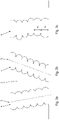
- figure 1 shows a flowchart with several method steps for making an opening in a plate-shaped workpiece by irradiation with laser radiation and subsequent etching with individual method steps when making an opening in a plate-shaped workpiece 1.
- a laser radiation 2 is directed onto the surface of the workpiece 1.
- the thickness d of the workpiece 1 is up to 3 mm.
- the exposure time of the laser radiation 2 is chosen to be extremely short, so that only a modification of the workpiece 1 occurs concentrically around a beam axis of the laser beam.
- the laser is operated with a wavelength for which the workpiece 1 is transparent.
- Such a modified area with defects 3 is in Figure 1b represented as a linear chain of bubbles.
- the opening has a plurality of circumferential, concentric structures on the lateral surface, as shown in the illustrations Figures 2a and 2b such as Figure 3a to 3c can be seen.
- the recess 4 is formed as a result of successive etching of a plurality of defects 3 lined up one behind the other, in that the previously produced defects 3, which are enlarged by the etching effect to form a cavity in the workpiece 1, are successively connected by the etching process.
- the etching liquid quickly moves from defect 3 to defect 3. Because the influence of gravity is not decisive here, the etching progresses both from above and from below and starts on both outer sides at the same time. Due to the relatively longer exposure time of the caustic medium in the area of the outside, it comes about
- the etching process follows a line 5 on which the defects 3 are arranged.
- the line 5 can be a straight line or follow almost any contour that is precisely maintained by the etching process. This makes it possible for the first time to produce almost any cutting contour.
- the contour of the recess 4 or opening produced in this way is characterized by a sequence of cross-sectional enlargements and constrictions, the shape of which is pronounced of an earthworm, with the cross-sectional enlargements and constrictions neither having a matching cross-sectional area, as for example in figures 2b and 3c to recognize, still have a matching distance a1, a2, to adjacent cross-sectional extensions and constrictions must have, as in the Figure 3c is shown.
- a cross-sectional expansion or constriction can be in a cross-sectional plane to the main axis or, as in the Figure 3a shown, be arranged inclined thereto.
- Neighboring cross-sectional enlargements or constrictions can also have centers that lie on a common line 5 that is inclined relative to the surface of the workpiece 1, so that the cross-sectional enlargements or constrictions are offset from one another, with the cross-sectional enlargements or constrictions as in FIG Figure 3a shown inclined to the outer surface or as in the Figure 3b shown can be aligned parallel to the outer surface.
- the respective centroids of adjacent cross-sectional extensions have an offset, so that they are in particular not arranged on a common straight line.
Landscapes
- Engineering & Computer Science (AREA)
- Physics & Mathematics (AREA)
- Optics & Photonics (AREA)
- Chemical & Material Sciences (AREA)
- Plasma & Fusion (AREA)
- Mechanical Engineering (AREA)
- Manufacturing & Machinery (AREA)
- Microelectronics & Electronic Packaging (AREA)
- Inorganic Chemistry (AREA)
- Materials Engineering (AREA)
- Life Sciences & Earth Sciences (AREA)
- Chemical Kinetics & Catalysis (AREA)
- General Chemical & Material Sciences (AREA)
- Geochemistry & Mineralogy (AREA)
- Organic Chemistry (AREA)
- Toxicology (AREA)
- Health & Medical Sciences (AREA)
- Laser Beam Processing (AREA)
- Ceramic Engineering (AREA)
- Surface Treatment Of Glass (AREA)
- Lead Frames For Integrated Circuits (AREA)
Applications Claiming Priority (4)
| Application Number | Priority Date | Filing Date | Title |
|---|---|---|---|
| DE102014113339.0A DE102014113339A1 (de) | 2014-09-16 | 2014-09-16 | Verfahren zur Erzeugung von Ausnehmungen in einem Material |
| DE102014116291 | 2014-11-07 | ||
| EP15762474.3A EP3195706B2 (fr) | 2014-09-16 | 2015-08-07 | Procédé d'insertion d'au moins un évidement ou trou débouchant dans une pièce en forme de plaque |
| PCT/DE2015/100333 WO2016041544A1 (fr) | 2014-09-16 | 2015-08-07 | Procédé d'insertion d'au moins un évidement ou trou débouchant dans une pièce en forme de plaque |
Related Parent Applications (2)
| Application Number | Title | Priority Date | Filing Date |
|---|---|---|---|
| EP15762474.3A Division EP3195706B2 (fr) | 2014-09-16 | 2015-08-07 | Procédé d'insertion d'au moins un évidement ou trou débouchant dans une pièce en forme de plaque |
| EP15762474.3A Division-Into EP3195706B2 (fr) | 2014-09-16 | 2015-08-07 | Procédé d'insertion d'au moins un évidement ou trou débouchant dans une pièce en forme de plaque |
Publications (1)
| Publication Number | Publication Date |
|---|---|
| EP4061101A1 true EP4061101A1 (fr) | 2022-09-21 |
Family
ID=54072638
Family Applications (2)
| Application Number | Title | Priority Date | Filing Date |
|---|---|---|---|
| EP22167179.5A Pending EP4061101A1 (fr) | 2014-09-16 | 2015-08-07 | Procédé de réalisation d'au moins un évidement ou un trou dans une pièce en forme de plaque |
| EP15762474.3A Active EP3195706B2 (fr) | 2014-09-16 | 2015-08-07 | Procédé d'insertion d'au moins un évidement ou trou débouchant dans une pièce en forme de plaque |
Family Applications After (1)
| Application Number | Title | Priority Date | Filing Date |
|---|---|---|---|
| EP15762474.3A Active EP3195706B2 (fr) | 2014-09-16 | 2015-08-07 | Procédé d'insertion d'au moins un évidement ou trou débouchant dans une pièce en forme de plaque |
Country Status (11)
| Country | Link |
|---|---|
| US (2) | US11610784B2 (fr) |
| EP (2) | EP4061101A1 (fr) |
| JP (2) | JP6782692B2 (fr) |
| KR (6) | KR20170044143A (fr) |
| CN (1) | CN107006128B (fr) |
| ES (1) | ES2923764T5 (fr) |
| LT (1) | LT3195706T (fr) |
| MY (1) | MY196621A (fr) |
| SG (2) | SG10201902331XA (fr) |
| TW (1) | TWI616939B (fr) |
| WO (1) | WO2016041544A1 (fr) |
Families Citing this family (22)
| Publication number | Priority date | Publication date | Assignee | Title |
|---|---|---|---|---|
| DE102018100299A1 (de) | 2017-01-27 | 2018-08-02 | Schott Ag | Strukturiertes plattenförmiges Glaselement und Verfahren zu dessen Herstellung |
| JP6898998B2 (ja) | 2017-03-06 | 2021-07-07 | エル・ピー・ケー・エフ・レーザー・ウント・エレクトロニクス・アクチエンゲゼルシヤフト | 電磁放射及び続くエッチングプロセスにより材料内に少なくとも1つの空隙を施すための方法 |
| WO2018162386A1 (fr) | 2017-03-06 | 2018-09-13 | Lpkf Laser & Electronics Ag | Procédé servant à fabriquer un masque technique |
| DE102018110211A1 (de) * | 2018-04-27 | 2019-10-31 | Schott Ag | Verfahren zum Erzeugen feiner Strukturen im Volumen eines Substrates aus sprödharten Material |
| TWI678342B (zh) | 2018-11-09 | 2019-12-01 | 財團法人工業技術研究院 | 形成導角的切割方法 |
| DE102020100848B4 (de) | 2019-01-29 | 2023-07-27 | Lpkf Laser & Electronics Aktiengesellschaft | Verfahren zur Mikrostrukturierung eines Glassubstrats mittels Laserstrahlung |
| DE102019201347B3 (de) * | 2019-02-01 | 2020-06-18 | Lpkf Laser & Electronics Ag | Herstellung von metallischen Leiterbahnen an Glas |
| CN113614045B (zh) * | 2019-02-08 | 2023-11-21 | 康宁股份有限公司 | 采用脉冲激光束聚焦线和气相蚀刻对透明工件进行激光加工的方法 |
| DE102019121827A1 (de) * | 2019-08-13 | 2021-02-18 | Trumpf Laser- Und Systemtechnik Gmbh | Laserätzen mit variierender Ätzselektivität |
| CN113594014B (zh) * | 2020-04-30 | 2024-04-12 | 中微半导体设备(上海)股份有限公司 | 零部件、等离子体反应装置及零部件加工方法 |
| DE102020114195A1 (de) | 2020-05-27 | 2021-12-02 | Lpkf Laser & Electronics Aktiengesellschaft | Verfahren zum Einbringen einer Ausnehmung in ein Substrat |
| DE102020118939A1 (de) | 2020-07-17 | 2022-01-20 | Schott Ag | Glaswafer und Glaselement für Drucksensoren |
| CN111799169B (zh) * | 2020-07-17 | 2024-05-28 | 绍兴同芯成集成电路有限公司 | 一种飞秒激光结合hf湿蚀刻加工tgv的工艺 |
| DE102020120370B3 (de) | 2020-08-03 | 2022-02-03 | Infineon Technologies Ag | Mems-sensor mit partikelfilter und verfahren zu seiner herstellung |
| KR20220019158A (ko) | 2020-08-06 | 2022-02-16 | 삼성디스플레이 주식회사 | 윈도우 및 이를 포함하는 표시장치 |
| EP4011846A1 (fr) | 2020-12-09 | 2022-06-15 | Schott Ag | Procédé de structuration d'un élément en verre et élément en verre structuré ainsi produit |
| DE102021204675B4 (de) | 2021-05-07 | 2023-05-17 | Lpkf Laser & Electronics Se | Vorrichtung und Verfahren zur Zellkultivierung |
| CN113510364B (zh) * | 2021-07-28 | 2022-11-25 | 广东工业大学 | 一种基于激光辅助溶解的三维空腔结构的成型方法 |
| EP4296244A1 (fr) | 2022-06-21 | 2023-12-27 | LPKF Laser & Electronics SE | Support de substrat en verre pour le traitement d'un substrat et procédé pour sa fabrication |
| DE102022127259B4 (de) | 2022-10-18 | 2026-02-12 | Lpkf Laser & Electronics Aktiengesellschaft | Verfahren sowie Vorrichtung zur Abbildung eines Strahls auf ein Objekt und Verfahren zum Einbringen einer Öffnung in ein Werkstück mittels dieses Verfahrens |
| DE102023125725A1 (de) * | 2023-09-22 | 2025-03-27 | Schott Ag | Laser-strukturiertes optisches Element |
| DE102024105120A1 (de) | 2024-02-23 | 2025-08-28 | Lpkf Laser & Electronics Se | Verfahren zur Integration und/oder Bearbeitung wenigstens eines Substrats sowie Substratstapel |
Citations (7)
| Publication number | Priority date | Publication date | Assignee | Title |
|---|---|---|---|---|
| WO2001015819A1 (fr) * | 1999-08-30 | 2001-03-08 | Board Of Regents University Of Nebraska-Lincoln | Interconnexions electriques en trois dimensions |
| DE102010025966B4 (de) | 2010-07-02 | 2012-03-08 | Schott Ag | Interposer und Verfahren zum Herstellen von Löchern in einem Interposer |
| US20120125887A1 (en) * | 2010-07-26 | 2012-05-24 | Hamamatsu Photonics K.K. | Method for manufacturing light-absorbing substrate and method for manufacturing mold for making same |
| US20120125893A1 (en) * | 2010-07-26 | 2012-05-24 | Hamamatsu Photonics K.K. | Laser processing method |
| US20120142186A1 (en) * | 2010-07-26 | 2012-06-07 | Hamamatsu Photonics K.K. | Method for manufacturing interposer |
| US20130029093A1 (en) * | 2010-04-08 | 2013-01-31 | Fujikura Ltd. | Method of forming microstructure, laser irradiation device, and substrate |
| US20130126573A1 (en) | 2010-07-12 | 2013-05-23 | Filaser Inc. | Method of material processing by laser filamentation |
Family Cites Families (13)
| Publication number | Priority date | Publication date | Assignee | Title |
|---|---|---|---|---|
| JP4880820B2 (ja) | 2001-01-19 | 2012-02-22 | 株式会社レーザーシステム | レーザ支援加工方法 |
| JP4418282B2 (ja) | 2004-03-31 | 2010-02-17 | 株式会社レーザーシステム | レーザ加工方法 |
| JP4222296B2 (ja) | 2004-11-22 | 2009-02-12 | 住友電気工業株式会社 | レーザ加工方法とレーザ加工装置 |
| US9138913B2 (en) | 2005-09-08 | 2015-09-22 | Imra America, Inc. | Transparent material processing with an ultrashort pulse laser |
| KR102035619B1 (ko) * | 2010-07-26 | 2019-12-16 | 하마마츠 포토닉스 가부시키가이샤 | 레이저 가공방법 |
| US8933367B2 (en) | 2011-02-09 | 2015-01-13 | Sumitomo Electric Industries, Ltd. | Laser processing method |
| JP6333282B2 (ja) * | 2012-11-29 | 2018-05-30 | コーニング インコーポレイテッド | レーザー損傷及びエッチングによってガラス物品を製造する方法 |
| EP2754524B1 (fr) | 2013-01-15 | 2015-11-25 | Corning Laser Technologies GmbH | Procédé et dispositif destinés au traitement basé sur laser de substrats plats, galette ou élément en verre, utilisant un faisceau laser en ligne |
| JP6113529B2 (ja) * | 2013-03-05 | 2017-04-12 | 株式会社ディスコ | ウエーハの加工方法 |
| DE102013223637B4 (de) † | 2013-11-20 | 2018-02-01 | Trumpf Laser- Und Systemtechnik Gmbh | Verfahren zum Behandeln eines lasertransparenten Substrats zum anschließenden Trennen des Substrats |
| US10293436B2 (en) * | 2013-12-17 | 2019-05-21 | Corning Incorporated | Method for rapid laser drilling of holes in glass and products made therefrom |
| JP2019535619A (ja) * | 2016-11-04 | 2019-12-12 | コーニング インコーポレイテッド | 微細穿孔板システム、用途、および微細穿孔板システムを作る方法 |
| US11344973B2 (en) * | 2018-04-19 | 2022-05-31 | Corning Incorporated | Methods for forming holes in substrates |
-
2015
- 2015-08-07 KR KR1020177007041A patent/KR20170044143A/ko not_active Ceased
- 2015-08-07 EP EP22167179.5A patent/EP4061101A1/fr active Pending
- 2015-08-07 WO PCT/DE2015/100333 patent/WO2016041544A1/fr not_active Ceased
- 2015-08-07 KR KR1020237018486A patent/KR102813417B1/ko active Active
- 2015-08-07 LT LTEPPCT/DE2015/100333T patent/LT3195706T/lt unknown
- 2015-08-07 KR KR1020257016919A patent/KR102851778B1/ko active Active
- 2015-08-07 ES ES15762474T patent/ES2923764T5/es active Active
- 2015-08-07 MY MYPI2017700845A patent/MY196621A/en unknown
- 2015-08-07 SG SG10201902331XA patent/SG10201902331XA/en unknown
- 2015-08-07 CN CN201580049903.1A patent/CN107006128B/zh active Active
- 2015-08-07 JP JP2017512917A patent/JP6782692B2/ja active Active
- 2015-08-07 KR KR1020257028228A patent/KR20250133802A/ko active Pending
- 2015-08-07 SG SG11201702091WA patent/SG11201702091WA/en unknown
- 2015-08-07 US US15/511,272 patent/US11610784B2/en active Active
- 2015-08-07 EP EP15762474.3A patent/EP3195706B2/fr active Active
- 2015-08-07 KR KR1020217005121A patent/KR20210022773A/ko not_active Ceased
- 2015-08-07 KR KR1020197015976A patent/KR20190065480A/ko not_active Ceased
- 2015-09-09 TW TW104129751A patent/TWI616939B/zh active
-
2020
- 2020-07-09 JP JP2020118488A patent/JP7049404B2/ja active Active
-
2022
- 2022-04-01 US US17/711,136 patent/US12604743B2/en active Active
Patent Citations (7)
| Publication number | Priority date | Publication date | Assignee | Title |
|---|---|---|---|---|
| WO2001015819A1 (fr) * | 1999-08-30 | 2001-03-08 | Board Of Regents University Of Nebraska-Lincoln | Interconnexions electriques en trois dimensions |
| US20130029093A1 (en) * | 2010-04-08 | 2013-01-31 | Fujikura Ltd. | Method of forming microstructure, laser irradiation device, and substrate |
| DE102010025966B4 (de) | 2010-07-02 | 2012-03-08 | Schott Ag | Interposer und Verfahren zum Herstellen von Löchern in einem Interposer |
| US20130126573A1 (en) | 2010-07-12 | 2013-05-23 | Filaser Inc. | Method of material processing by laser filamentation |
| US20120125887A1 (en) * | 2010-07-26 | 2012-05-24 | Hamamatsu Photonics K.K. | Method for manufacturing light-absorbing substrate and method for manufacturing mold for making same |
| US20120125893A1 (en) * | 2010-07-26 | 2012-05-24 | Hamamatsu Photonics K.K. | Laser processing method |
| US20120142186A1 (en) * | 2010-07-26 | 2012-06-07 | Hamamatsu Photonics K.K. | Method for manufacturing interposer |
Also Published As
| Publication number | Publication date |
|---|---|
| KR20190065480A (ko) | 2019-06-11 |
| SG11201702091WA (en) | 2017-04-27 |
| EP3195706A1 (fr) | 2017-07-26 |
| CN107006128A (zh) | 2017-08-01 |
| CN107006128B (zh) | 2020-05-19 |
| LT3195706T (lt) | 2022-08-10 |
| KR20250133802A (ko) | 2025-09-08 |
| ES2923764T5 (en) | 2025-10-09 |
| ES2923764T3 (es) | 2022-09-30 |
| TWI616939B (zh) | 2018-03-01 |
| US20220223434A1 (en) | 2022-07-14 |
| US11610784B2 (en) | 2023-03-21 |
| JP2020185613A (ja) | 2020-11-19 |
| KR102813417B1 (ko) | 2025-05-29 |
| EP3195706B1 (fr) | 2022-06-01 |
| TW201621986A (zh) | 2016-06-16 |
| KR20210022773A (ko) | 2021-03-03 |
| KR20170044143A (ko) | 2017-04-24 |
| JP2017534458A (ja) | 2017-11-24 |
| KR20230084606A (ko) | 2023-06-13 |
| JP6782692B2 (ja) | 2020-11-11 |
| JP7049404B2 (ja) | 2022-04-06 |
| US12604743B2 (en) | 2026-04-14 |
| MY196621A (en) | 2023-04-23 |
| KR102851778B1 (ko) | 2025-09-01 |
| US20170256422A1 (en) | 2017-09-07 |
| EP3195706B2 (fr) | 2025-05-14 |
| WO2016041544A1 (fr) | 2016-03-24 |
| KR20250079054A (ko) | 2025-06-04 |
| SG10201902331XA (en) | 2019-04-29 |
Similar Documents
| Publication | Publication Date | Title |
|---|---|---|
| EP3195706B1 (fr) | Procédé d'insertion d'au moins un évidement ou trou débouchant dans une pièce en forme de plaque | |
| EP2964417B1 (fr) | Procédé permettant de pratiquer des perforations dans un substrat | |
| EP2964416B1 (fr) | Procédé de séparation d'un substrat | |
| DE102014113339A1 (de) | Verfahren zur Erzeugung von Ausnehmungen in einem Material | |
| DE102018110211A1 (de) | Verfahren zum Erzeugen feiner Strukturen im Volumen eines Substrates aus sprödharten Material | |
| DE102013103370A1 (de) | Verfahren zum Einbringen von Durchbrechungen in ein Glassubstrat sowie ein derart hergestelltes Glassubstrat | |
| WO2018162385A1 (fr) | Procédé de réalisation d'au moins un évidement dans un matériau à l'aide d'un rayonnement électromagnétique et d'un procédé de gravure consécutif | |
| EP4013716B1 (fr) | Procédé pour usiner une pièce | |
| WO2021191218A1 (fr) | Procédé, système et pièce avec enlèvement d'un gros volume de matière de la pièce par gravure assistée par laser | |
| EP4380903A1 (fr) | Procédé et dispositif d'usinage au laser d'une pièce | |
| DE102020114195A1 (de) | Verfahren zum Einbringen einer Ausnehmung in ein Substrat | |
| DE19535666C2 (de) | Verfahren zur Erzeugung einer Feinkeramikstruktur | |
| DE102017106372A1 (de) | Verfahren zur Bearbeitung eines Werkstückes und ein dadurch hergestelltes Werkstück | |
| EP4288235A1 (fr) | Dispositif et procédé d'usinage au laser d'une pièce | |
| DE102021123801A1 (de) | Verfahren und Vorrichtung zur Laserbearbeitung eines Werkstücks | |
| EP3875436B1 (fr) | Procédé de préparation et/ou de mise en uvre de la séparation d'un élément de substrat et élément de substrat | |
| DE102010032029B4 (de) | Verfahren zum Trennen einer runden Planplatte aus sprödbrüchigem Material in mehrere rechteckige Einzelplatten mittels Laser | |
| EP3966157B1 (fr) | Procédé de production de microstructures dans un substrat de verre | |
| EP4514760A1 (fr) | Procédé de séparation d'une pièce de travail | |
| WO2023088912A1 (fr) | Procédé pour le traitement laser d'une pièce | |
| EP4402108A1 (fr) | Procédé et dispositif d'usinage au laser d?une pièce | |
| DE102021108505A1 (de) | Vorrichtung und Verfahren zur Laserbearbeitung eines Werkstücks | |
| DE102024119224A1 (de) | Verfahren zum Bearbeiten eines Werkstücks aus sprödhartem Material | |
| DE102024122506A1 (de) | Verfahren zur Herstellung eines Bauteils aus einem Substrat sowie Bauteil | |
| EP4079443A1 (fr) | Procédé de vérification d'une distribution d'énergie appliquée au moyen d'un foyer linéaire d'un faisceau laser à l'intérieure d'un substrat et substrat |
Legal Events
| Date | Code | Title | Description |
|---|---|---|---|
| PUAI | Public reference made under article 153(3) epc to a published international application that has entered the european phase |
Free format text: ORIGINAL CODE: 0009012 |
|
| STAA | Information on the status of an ep patent application or granted ep patent |
Free format text: STATUS: THE APPLICATION HAS BEEN PUBLISHED |
|
| AC | Divisional application: reference to earlier application |
Ref document number: 3195706 Country of ref document: EP Kind code of ref document: P |
|
| AK | Designated contracting states |
Kind code of ref document: A1 Designated state(s): AL AT BE BG CH CY CZ DE DK EE ES FI FR GB GR HR HU IE IS IT LI LT LU LV MC MK MT NL NO PL PT RO RS SE SI SK SM TR |
|
| STAA | Information on the status of an ep patent application or granted ep patent |
Free format text: STATUS: REQUEST FOR EXAMINATION WAS MADE |
|
| 17P | Request for examination filed |
Effective date: 20221121 |
|
| RBV | Designated contracting states (corrected) |
Designated state(s): AL AT BE BG CH CY CZ DE DK EE ES FI FR GB GR HR HU IE IS IT LI LT LU LV MC MK MT NL NO PL PT RO RS SE SI SK SM TR |
|
| RAP3 | Party data changed (applicant data changed or rights of an application transferred) |
Owner name: LPKF LASER & ELECTRONICS SE |
|
| STAA | Information on the status of an ep patent application or granted ep patent |
Free format text: STATUS: EXAMINATION IS IN PROGRESS |
|
| 17Q | First examination report despatched |
Effective date: 20230928 |
|
| TPAC | Observations filed by third parties |
Free format text: ORIGINAL CODE: EPIDOSNTIPA |