EP4063044A1 - Matériau de cuisson de type film, matériau de cuisson de type film avec feuille de support, corps multicouche et procédé de production de dispositif - Google Patents
Matériau de cuisson de type film, matériau de cuisson de type film avec feuille de support, corps multicouche et procédé de production de dispositif Download PDFInfo
- Publication number
- EP4063044A1 EP4063044A1 EP20889717.3A EP20889717A EP4063044A1 EP 4063044 A1 EP4063044 A1 EP 4063044A1 EP 20889717 A EP20889717 A EP 20889717A EP 4063044 A1 EP4063044 A1 EP 4063044A1
- Authority
- EP
- European Patent Office
- Prior art keywords
- film
- firing material
- shaped firing
- support sheet
- shaped
- Prior art date
- Legal status (The legal status is an assumption and is not a legal conclusion. Google has not performed a legal analysis and makes no representation as to the accuracy of the status listed.)
- Withdrawn
Links
Images


Classifications
-
- H—ELECTRICITY
- H10—SEMICONDUCTOR DEVICES; ELECTRIC SOLID-STATE DEVICES NOT OTHERWISE PROVIDED FOR
- H10P—GENERIC PROCESSES OR APPARATUS FOR THE MANUFACTURE OR TREATMENT OF DEVICES COVERED BY CLASS H10
- H10P72/00—Handling or holding of wafers, substrates or devices during manufacture or treatment thereof
- H10P72/70—Handling or holding of wafers, substrates or devices during manufacture or treatment thereof for supporting or gripping
- H10P72/74—Handling or holding of wafers, substrates or devices during manufacture or treatment thereof for supporting or gripping using temporarily an auxiliary support
- H10P72/7402—Wafer tapes, e.g. grinding or dicing support tapes
-
- B—PERFORMING OPERATIONS; TRANSPORTING
- B22—CASTING; POWDER METALLURGY
- B22F—WORKING METALLIC POWDER; MANUFACTURE OF ARTICLES FROM METALLIC POWDER; MAKING METALLIC POWDER; APPARATUS OR DEVICES SPECIALLY ADAPTED FOR METALLIC POWDER
- B22F1/00—Metallic powder; Treatment of metallic powder, e.g. to facilitate working or to improve properties
- B22F1/10—Metallic powder containing lubricating or binding agents; Metallic powder containing organic material
-
- B—PERFORMING OPERATIONS; TRANSPORTING
- B22—CASTING; POWDER METALLURGY
- B22F—WORKING METALLIC POWDER; MANUFACTURE OF ARTICLES FROM METALLIC POWDER; MAKING METALLIC POWDER; APPARATUS OR DEVICES SPECIALLY ADAPTED FOR METALLIC POWDER
- B22F7/00—Manufacture of composite layers, workpieces, or articles, comprising metallic powder, by sintering the powder, with or without compacting wherein at least one part is obtained by sintering or compression
- B22F7/06—Manufacture of composite layers, workpieces, or articles, comprising metallic powder, by sintering the powder, with or without compacting wherein at least one part is obtained by sintering or compression of composite workpieces or articles from parts, e.g. to form tipped tools
- B22F7/062—Manufacture of composite layers, workpieces, or articles, comprising metallic powder, by sintering the powder, with or without compacting wherein at least one part is obtained by sintering or compression of composite workpieces or articles from parts, e.g. to form tipped tools involving the connection or repairing of preformed parts
-
- B—PERFORMING OPERATIONS; TRANSPORTING
- B22—CASTING; POWDER METALLURGY
- B22F—WORKING METALLIC POWDER; MANUFACTURE OF ARTICLES FROM METALLIC POWDER; MAKING METALLIC POWDER; APPARATUS OR DEVICES SPECIALLY ADAPTED FOR METALLIC POWDER
- B22F7/00—Manufacture of composite layers, workpieces, or articles, comprising metallic powder, by sintering the powder, with or without compacting wherein at least one part is obtained by sintering or compression
- B22F7/06—Manufacture of composite layers, workpieces, or articles, comprising metallic powder, by sintering the powder, with or without compacting wherein at least one part is obtained by sintering or compression of composite workpieces or articles from parts, e.g. to form tipped tools
- B22F7/08—Manufacture of composite layers, workpieces, or articles, comprising metallic powder, by sintering the powder, with or without compacting wherein at least one part is obtained by sintering or compression of composite workpieces or articles from parts, e.g. to form tipped tools with one or more parts not made from powder
-
- B—PERFORMING OPERATIONS; TRANSPORTING
- B22—CASTING; POWDER METALLURGY
- B22F—WORKING METALLIC POWDER; MANUFACTURE OF ARTICLES FROM METALLIC POWDER; MAKING METALLIC POWDER; APPARATUS OR DEVICES SPECIALLY ADAPTED FOR METALLIC POWDER
- B22F9/00—Making metallic powder or suspensions thereof
-
- C—CHEMISTRY; METALLURGY
- C08—ORGANIC MACROMOLECULAR COMPOUNDS; THEIR PREPARATION OR CHEMICAL WORKING-UP; COMPOSITIONS BASED THEREON
- C08K—Use of inorganic or non-macromolecular organic substances as compounding ingredients
- C08K3/00—Use of inorganic substances as compounding ingredients
- C08K3/02—Elements
- C08K3/08—Metals
-
- C—CHEMISTRY; METALLURGY
- C08—ORGANIC MACROMOLECULAR COMPOUNDS; THEIR PREPARATION OR CHEMICAL WORKING-UP; COMPOSITIONS BASED THEREON
- C08K—Use of inorganic or non-macromolecular organic substances as compounding ingredients
- C08K5/00—Use of organic ingredients
- C08K5/04—Oxygen-containing compounds
- C08K5/10—Esters; Ether-esters
- C08K5/11—Esters; Ether-esters of acyclic polycarboxylic acids
-
- C—CHEMISTRY; METALLURGY
- C08—ORGANIC MACROMOLECULAR COMPOUNDS; THEIR PREPARATION OR CHEMICAL WORKING-UP; COMPOSITIONS BASED THEREON
- C08K—Use of inorganic or non-macromolecular organic substances as compounding ingredients
- C08K9/00—Use of pretreated ingredients
- C08K9/04—Ingredients treated with organic substances
-
- H—ELECTRICITY
- H10—SEMICONDUCTOR DEVICES; ELECTRIC SOLID-STATE DEVICES NOT OTHERWISE PROVIDED FOR
- H10P—GENERIC PROCESSES OR APPARATUS FOR THE MANUFACTURE OR TREATMENT OF DEVICES COVERED BY CLASS H10
- H10P54/00—Cutting or separating of wafers, substrates or parts of devices
-
- H—ELECTRICITY
- H10—SEMICONDUCTOR DEVICES; ELECTRIC SOLID-STATE DEVICES NOT OTHERWISE PROVIDED FOR
- H10W—GENERIC PACKAGES, INTERCONNECTIONS, CONNECTORS OR OTHER CONSTRUCTIONAL DETAILS OF DEVICES COVERED BY CLASS H10
- H10W72/00—Interconnections or connectors in packages
- H10W72/071—Connecting or disconnecting
-
- H—ELECTRICITY
- H10—SEMICONDUCTOR DEVICES; ELECTRIC SOLID-STATE DEVICES NOT OTHERWISE PROVIDED FOR
- H10W—GENERIC PACKAGES, INTERCONNECTIONS, CONNECTORS OR OTHER CONSTRUCTIONAL DETAILS OF DEVICES COVERED BY CLASS H10
- H10W72/00—Interconnections or connectors in packages
- H10W72/30—Die-attach connectors
-
- B—PERFORMING OPERATIONS; TRANSPORTING
- B22—CASTING; POWDER METALLURGY
- B22F—WORKING METALLIC POWDER; MANUFACTURE OF ARTICLES FROM METALLIC POWDER; MAKING METALLIC POWDER; APPARATUS OR DEVICES SPECIALLY ADAPTED FOR METALLIC POWDER
- B22F1/00—Metallic powder; Treatment of metallic powder, e.g. to facilitate working or to improve properties
- B22F1/05—Metallic powder characterised by the size or surface area of the particles
- B22F1/054—Nanosized particles
- B22F1/0545—Dispersions or suspensions of nanosized particles
-
- B—PERFORMING OPERATIONS; TRANSPORTING
- B22—CASTING; POWDER METALLURGY
- B22F—WORKING METALLIC POWDER; MANUFACTURE OF ARTICLES FROM METALLIC POWDER; MAKING METALLIC POWDER; APPARATUS OR DEVICES SPECIALLY ADAPTED FOR METALLIC POWDER
- B22F1/00—Metallic powder; Treatment of metallic powder, e.g. to facilitate working or to improve properties
- B22F1/10—Metallic powder containing lubricating or binding agents; Metallic powder containing organic material
- B22F1/102—Metallic powder coated with organic material
-
- B—PERFORMING OPERATIONS; TRANSPORTING
- B22—CASTING; POWDER METALLURGY
- B22F—WORKING METALLIC POWDER; MANUFACTURE OF ARTICLES FROM METALLIC POWDER; MAKING METALLIC POWDER; APPARATUS OR DEVICES SPECIALLY ADAPTED FOR METALLIC POWDER
- B22F2301/00—Metallic composition of the powder or its coating
- B22F2301/25—Noble metals, i.e. Ag Au, Ir, Os, Pd, Pt, Rh, Ru
- B22F2301/255—Silver or gold
-
- B—PERFORMING OPERATIONS; TRANSPORTING
- B22—CASTING; POWDER METALLURGY
- B22F—WORKING METALLIC POWDER; MANUFACTURE OF ARTICLES FROM METALLIC POWDER; MAKING METALLIC POWDER; APPARATUS OR DEVICES SPECIALLY ADAPTED FOR METALLIC POWDER
- B22F2999/00—Aspects linked to processes or compositions used in powder metallurgy
-
- B—PERFORMING OPERATIONS; TRANSPORTING
- B82—NANOTECHNOLOGY
- B82Y—SPECIFIC USES OR APPLICATIONS OF NANOSTRUCTURES; MEASUREMENT OR ANALYSIS OF NANOSTRUCTURES; MANUFACTURE OR TREATMENT OF NANOSTRUCTURES
- B82Y30/00—Nanotechnology for materials or surface science, e.g. nanocomposites
-
- C—CHEMISTRY; METALLURGY
- C08—ORGANIC MACROMOLECULAR COMPOUNDS; THEIR PREPARATION OR CHEMICAL WORKING-UP; COMPOSITIONS BASED THEREON
- C08K—Use of inorganic or non-macromolecular organic substances as compounding ingredients
- C08K3/00—Use of inorganic substances as compounding ingredients
- C08K3/02—Elements
- C08K3/08—Metals
- C08K2003/0806—Silver
-
- H—ELECTRICITY
- H10—SEMICONDUCTOR DEVICES; ELECTRIC SOLID-STATE DEVICES NOT OTHERWISE PROVIDED FOR
- H10P—GENERIC PROCESSES OR APPARATUS FOR THE MANUFACTURE OR TREATMENT OF DEVICES COVERED BY CLASS H10
- H10P72/00—Handling or holding of wafers, substrates or devices during manufacture or treatment thereof
- H10P72/70—Handling or holding of wafers, substrates or devices during manufacture or treatment thereof for supporting or gripping
- H10P72/74—Handling or holding of wafers, substrates or devices during manufacture or treatment thereof for supporting or gripping using temporarily an auxiliary support
- H10P72/7412—Handling or holding of wafers, substrates or devices during manufacture or treatment thereof for supporting or gripping using temporarily an auxiliary support the auxiliary support including means facilitating the separation of a device or wafer from the auxiliary support
- H10P72/7414—Handling or holding of wafers, substrates or devices during manufacture or treatment thereof for supporting or gripping using temporarily an auxiliary support the auxiliary support including means facilitating the separation of a device or wafer from the auxiliary support the auxiliary support including means facilitating the selective separation of some of a plurality of devices from the auxiliary support
-
- H—ELECTRICITY
- H10—SEMICONDUCTOR DEVICES; ELECTRIC SOLID-STATE DEVICES NOT OTHERWISE PROVIDED FOR
- H10P—GENERIC PROCESSES OR APPARATUS FOR THE MANUFACTURE OR TREATMENT OF DEVICES COVERED BY CLASS H10
- H10P72/00—Handling or holding of wafers, substrates or devices during manufacture or treatment thereof
- H10P72/70—Handling or holding of wafers, substrates or devices during manufacture or treatment thereof for supporting or gripping
- H10P72/74—Handling or holding of wafers, substrates or devices during manufacture or treatment thereof for supporting or gripping using temporarily an auxiliary support
- H10P72/7416—Handling or holding of wafers, substrates or devices during manufacture or treatment thereof for supporting or gripping using temporarily an auxiliary support used during dicing or grinding
-
- H—ELECTRICITY
- H10—SEMICONDUCTOR DEVICES; ELECTRIC SOLID-STATE DEVICES NOT OTHERWISE PROVIDED FOR
- H10P—GENERIC PROCESSES OR APPARATUS FOR THE MANUFACTURE OR TREATMENT OF DEVICES COVERED BY CLASS H10
- H10P72/00—Handling or holding of wafers, substrates or devices during manufacture or treatment thereof
- H10P72/70—Handling or holding of wafers, substrates or devices during manufacture or treatment thereof for supporting or gripping
- H10P72/74—Handling or holding of wafers, substrates or devices during manufacture or treatment thereof for supporting or gripping using temporarily an auxiliary support
- H10P72/7416—Handling or holding of wafers, substrates or devices during manufacture or treatment thereof for supporting or gripping using temporarily an auxiliary support used during dicing or grinding
- H10P72/7418—Handling or holding of wafers, substrates or devices during manufacture or treatment thereof for supporting or gripping using temporarily an auxiliary support used during dicing or grinding of passive members, e.g. a chip mounting substrate
-
- H—ELECTRICITY
- H10—SEMICONDUCTOR DEVICES; ELECTRIC SOLID-STATE DEVICES NOT OTHERWISE PROVIDED FOR
- H10P—GENERIC PROCESSES OR APPARATUS FOR THE MANUFACTURE OR TREATMENT OF DEVICES COVERED BY CLASS H10
- H10P72/00—Handling or holding of wafers, substrates or devices during manufacture or treatment thereof
- H10P72/70—Handling or holding of wafers, substrates or devices during manufacture or treatment thereof for supporting or gripping
- H10P72/74—Handling or holding of wafers, substrates or devices during manufacture or treatment thereof for supporting or gripping using temporarily an auxiliary support
- H10P72/744—Details of chemical or physical process used for separating the auxiliary support from a device or a wafer
-
- H—ELECTRICITY
- H10—SEMICONDUCTOR DEVICES; ELECTRIC SOLID-STATE DEVICES NOT OTHERWISE PROVIDED FOR
- H10P—GENERIC PROCESSES OR APPARATUS FOR THE MANUFACTURE OR TREATMENT OF DEVICES COVERED BY CLASS H10
- H10P72/00—Handling or holding of wafers, substrates or devices during manufacture or treatment thereof
- H10P72/70—Handling or holding of wafers, substrates or devices during manufacture or treatment thereof for supporting or gripping
- H10P72/74—Handling or holding of wafers, substrates or devices during manufacture or treatment thereof for supporting or gripping using temporarily an auxiliary support
- H10P72/744—Details of chemical or physical process used for separating the auxiliary support from a device or a wafer
- H10P72/7442—Separation by peeling
-
- H—ELECTRICITY
- H10—SEMICONDUCTOR DEVICES; ELECTRIC SOLID-STATE DEVICES NOT OTHERWISE PROVIDED FOR
- H10W—GENERIC PACKAGES, INTERCONNECTIONS, CONNECTORS OR OTHER CONSTRUCTIONAL DETAILS OF DEVICES COVERED BY CLASS H10
- H10W72/00—Interconnections or connectors in packages
- H10W72/01—Manufacture or treatment
- H10W72/013—Manufacture or treatment of die-attach connectors
- H10W72/01304—Manufacture or treatment of die-attach connectors using temporary auxiliary members, e.g. using sacrificial coatings or handle substrates
-
- H—ELECTRICITY
- H10—SEMICONDUCTOR DEVICES; ELECTRIC SOLID-STATE DEVICES NOT OTHERWISE PROVIDED FOR
- H10W—GENERIC PACKAGES, INTERCONNECTIONS, CONNECTORS OR OTHER CONSTRUCTIONAL DETAILS OF DEVICES COVERED BY CLASS H10
- H10W72/00—Interconnections or connectors in packages
- H10W72/01—Manufacture or treatment
- H10W72/013—Manufacture or treatment of die-attach connectors
- H10W72/01331—Manufacture or treatment of die-attach connectors using blanket deposition
- H10W72/01336—Manufacture or treatment of die-attach connectors using blanket deposition in solid form, e.g. by using a powder or by laminating a foil
-
- H—ELECTRICITY
- H10—SEMICONDUCTOR DEVICES; ELECTRIC SOLID-STATE DEVICES NOT OTHERWISE PROVIDED FOR
- H10W—GENERIC PACKAGES, INTERCONNECTIONS, CONNECTORS OR OTHER CONSTRUCTIONAL DETAILS OF DEVICES COVERED BY CLASS H10
- H10W72/00—Interconnections or connectors in packages
- H10W72/01—Manufacture or treatment
- H10W72/0198—Manufacture or treatment batch processes
-
- H—ELECTRICITY
- H10—SEMICONDUCTOR DEVICES; ELECTRIC SOLID-STATE DEVICES NOT OTHERWISE PROVIDED FOR
- H10W—GENERIC PACKAGES, INTERCONNECTIONS, CONNECTORS OR OTHER CONSTRUCTIONAL DETAILS OF DEVICES COVERED BY CLASS H10
- H10W72/00—Interconnections or connectors in packages
- H10W72/071—Connecting or disconnecting
- H10W72/073—Connecting or disconnecting of die-attach connectors
- H10W72/07331—Connecting techniques
Definitions
- a binder component may be blended into the firing material, and then the firing material may be formed into a film shape.
- the film-shaped firing material preferably has a high content of sinterable metal particles and a low content of the binder component.
- Fig. 1 is a cross-sectional view schematically illustrating a film-shaped firing material according to the present embodiment.
- a film-shaped firing material 1 contains sinterable metal particles 10, a binder component 20, and a liquid component 30.
- Crosslinked films of these may also be used. Laminated films of these may also be used. In addition, films obtained by coloring these, non-transparent films thereof, or the like can also be used.
- the release agent include silicone-based release agents, fluorine-based release agents, olefin-based release agents, alkyd-based release agents, and long-chain alkyl group-containing carbamates.
- the sinterable metal particles are preferably silver nanoparticles, which are nano-sized silver particles.
- a particle size of the sinterable metal particles contained in the film-shaped firing material is not limited as long as it is 100 nm or less and is a value at which the sinterable metal particles can exhibit the sinterability, but the particle size of the sinterable metal particles may be 50 nm or less, or 30 nm or less.
- the particle diameter of the metal particles contained in the film-shaped firing material is the projected area circle equivalent diameter of the particle diameter of the metal particles observed with an electron microscope. Metal particles that fall within the above range of particle diameters are preferable because they have excellent sinterability.
- non-sinterable metal particles In addition to the metal particles (sinterable metal particles) having a particle size of 100 nm or less, non-sinterable metal particles with a particle size of greater than 100 nm other than the sinterable metal particles may be further blended in the film-shaped firing material according to the present embodiment.
- the non-sinterable metal particles are particles that are more difficult to sinter than the aforementioned sinterable metal particles.
- non-sinterable metal particles specifically refers to particles containing a metal element having a particle size of greater than 100 nm.
- the number-average particle diameter of metal particles observed with an electron microscope may be greater than 150 nm and less than or equal to 50000 nm, may be from 150 to 10000 nm, or may be from 180 to 5000 nm.
- the quantity of metal particles to be measured is 100 or more per one film-shaped firing material, with the metal particles thereof being randomly selected.
- the metal particles to be measured are 100 metal particles randomly selected per film-shaped firing material.
- the sinterable metal particles having a particle size of 100 nm or less and the non-sinterable metal particles having a particle size of greater than 100 nm may be the same as each other or may be different from each other.
- the sinterable metal particles having a particle size of 100 nm or less may be silver particles, while the non-sinterable metal particles having a particle size of greater than 100 nm may be silver or silver oxide particles.
- the sinterable metal particles having a particle size of 100 nm or less may be silver or silver oxide particles, while the non-sinterable metal particles having a particle size of greater than 100 nm may be copper or copper oxide particles.
- mass average molecular weight refers to a polystyrene equivalent value measured by gel permeation chromatography (GPC).
- solvent means a substance that is in a liquid state at room temperature and has a boiling point of lower than 300°C.
- the film-shaped firing material may be composed of sinterable metal particles, non-sinterable metal particles, a binder component, a liquid component, and another additive, and the sum of contents (mass%) of these may be 100 mass%.
- the film-shaped firing material according to the present embodiment described above has a shape of a film, and thus the thickness is even.
- the film-shaped firing material according to the present embodiment contains a liquid component that is a liquid at room temperature and has a boiling point of from 300 to 450°C.
- the film-shaped firing material according to the present embodiment has a sufficient adhesive force with a support sheet and an excellent dicing suitability; meanwhile, the exuding of the film-shaped firing material from between a semiconductor chip and a substrate when the chip and the substrate are subjected to sinter bonding is suppressed.
- the boiling point exceeds 280°C, the solvent is less likely to volatilize in the volatilization and drying after printing; as a result, it may be difficult to ensure a desired shape, or the solvent may remain in the film during firing, which may degrade bonding adhesiveness.
- the boiling point is lower than 65°C, the solvent is volatilized during printing, and the stability of the thickness may be impaired.
- a solvent with a boiling point of from 200 to 280°C is used, an increase in viscosity caused by volatilization of the solvent during printing can be suppressed, and printing suitability can be obtained.
- the film-shaped firing material with a support sheet includes the film-shaped firing material described above and the support sheet provided on at least one side (surface) of the film-shaped firing material.
- the support sheet is one in which a pressure sensitive adhesive layer is provided on the entire surface or the outer circumferential section of a base material film, and the film-shaped firing material is preferably provided on the pressure sensitive adhesive layer.
- the film-shaped firing material may be provided in direct contact with the pressure sensitive adhesive layer, or may be provided in direct contact with the base material film. By adopting this configuration, the film-shaped firing material with a support sheet can be used as a dicing sheet that is used when dividing a semiconductor wafer into individual chips.
- this configuration allows the film-shaped firing material to be processed into the same shape as a chip when the film-shaped firing material is divided into individual pieces together with a semiconductor wafer with the use of a blade or the like, and thereby a semiconductor chip with film-shaped firing material can be produced.
- FIG. 2 and Fig. 3 are schematic cross-sectional views of the film-shaped firing material with a support sheet according to the present embodiment.
- a film-shaped firing material 1 is temporarily attached, in a releasable manner, to an inner circumferential section of a support sheet 2 having a pressure sensitive adhesion portion on an outer circumferential section.
- Fig. 2 and Fig. 3 are schematic cross-sectional views of the film-shaped firing material with a support sheet according to the present embodiment.
- 100a and 100b which are the film-shaped firing materials with a support sheet according to the present embodiment
- a film-shaped firing material 1 is temporarily attached, in a releasable manner, to an inner circumferential section of a support sheet 2 having a pressure sensitive adhesion portion on an outer circumferential section.
- the support sheet 2 has a configuration in which the support sheet 2 is a pressure sensitive adhesive sheet having a pressure sensitive adhesive layer 4 and a base material film 3, the pressure sensitive adhesive layer 4 being on the upper surface of the base material film 3, wherein the surface of the inner circumferential section of the pressure sensitive adhesive layer 4 is covered by the film-shaped firing material while the pressure sensitive adhesion portion is exposed at the outer circumferential section of the pressure sensitive adhesive layer 4. Further, as illustrated in Fig.
- a gravure coater, a Mayer bar coater, an air knife coater, a roll coater, or the like is used to coat the surface with the release agent as is without a solvent or diluted with a solvent or in the form of an emulsion, and the base material film coated with the release agent is then supplied at ordinary temperature or under heating, or is cured by an electron beam, or a laminate may be formed by wet lamination, dry lamination, hot-melt lamination, melt-extrusion lamination, coextrusion, or the like.
- the support sheet 2 has a pressure sensitive adhesion portion on at least the outer circumferential section thereof.
- the pressure sensitive adhesion portion has a function of temporarily fixing the ring frame 5 to the outer circumferential section of the film-shaped firing materials with a support sheet 100a and 100b, and the ring frame 5 preferably can be released after the required steps. Therefore, a pressure sensitive adhesive with weak adhesiveness may be used in the pressure sensitive adhesive layer 4, or an energy ray-curable pressure sensitive adhesive in which adhesive force is reduced by energy ray irradiation may be used.
- a re-releasable pressure sensitive adhesive layer can be formed from a variety of commonly known pressure sensitive adhesives (for example, a general purpose pressure sensitive adhesive such as a rubber adhesive, an acrylic adhesive, a silicone adhesive, a urethane adhesive, and a vinyl ether adhesive; a pressure sensitive adhesive with surface irregularities; an energy ray-curable pressure sensitive adhesive, and a pressure sensitive adhesive containing a thermally expanding component).
- a general purpose pressure sensitive adhesive such as a rubber adhesive, an acrylic adhesive, a silicone adhesive, a urethane adhesive, and a vinyl ether adhesive
- a pressure sensitive adhesive with surface irregularities such as an energy ray-curable pressure sensitive adhesive, and a pressure sensitive adhesive containing a thermally expanding component.
- an acrylic adhesive or a silicone adhesive is preferably used as the weak pressure sensitive adhesive.
- an adhesive force of the pressure sensitive adhesive layer 4 to a SUS board at 23°C is preferably from 30 to 120 mN/25 mm, more preferably from 50 to 100 mN/25 mm, and even more preferably from 60 to 90 mN/25 mm.
- the adhesive force is too weak, the ring frame may fall off.
- the adhesive force is too strong, releasing from the ring frame becomes difficult, and reuse of the ring frame also becomes difficult.
- the adhesive force is greater than or equal to the lower limit of the range, it is possible to suppress the falling off of the ring frame.
- the adhesive force is less than or equal to the upper limit of the range, releasing from the ring frame becomes easy, and reuse of the ring frame also becomes easy.
- the surface of the base material film 3 on which the pressure sensitive adhesive layer 4 is provided may be subjected, as desired, to an unevenness-forming treatment through sandblasting, a solvent treatment, or the like, or may be subjected to a treatment such as a corona discharge treatment, electron beam irradiation, a plasma treatment, an ozone/ultraviolet irradiation treatment, a flame treatment, a chromic acid treatment, a hot air treatment, or other such oxidizing treatment.
- the surface thereof may also be subjected to a primer treatment.
- Fig. 5 is a cross-sectional view schematically illustrating a laminate according to an embodiment of the present invention.
- a laminate 120 a film-shaped firing material with a support sheet 100 and a semiconductor wafer 18 are laminated, and a support sheet 2, a film-shaped firing material 1, and the semiconductor wafer 18 are laminated in this order.
- the semiconductor wafer 18 may be provided in direct contact with the film-shaped firing material 1.
- the film-shaped firing material with a support sheet according to the present embodiment contains a liquid component that is a liquid at room temperature and has a boiling point of from 300 to 450°C; as such, the adhesive force between the film-shaped firing material and the support sheet is sufficient during dicing, making it possible to prevent dicing defects such as chipping or scattering of the chips, achieving an excellent dicing suitability.
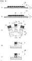
- Fig. 6(c) illustrates an example in which a protuberance (pin) 70 is projected from a raised portion (not illustrated) of a device for producing a semiconductor device, a tip end of the protuberance 70 pushes the laminate 120 upward from the side of the base material film 3, and thereby a force is applied in the projection direction of the protuberance 70 to the laminate 120 on which the cuts C and the semiconductor chip 19 have been formed.
- push-up conditions such as the projection amount (push-up amount) of the protuberance 70, the projection speed (push-up speed), and the holding time (push-up wait time) in the projected state can be adjusted as appropriate.
- the number of protuberances 70 is not particularly limited, and may be selected as appropriate.
- the film-shaped firing material may be fired through pressurized firing in which the film-shaped firing material is fired with pressure being applied.
- An example of a pressurizing condition is approximately from 0.1 to 50 MPa, preferably from 0.5 to 30 MPa, and more preferably from 1.0 to 20 MPa.
- a second embodiment of the method for producing a device according to the present invention includes affixing a semiconductor chip with film-shaped firing material, obtained by affixing a semiconductor chip to the film-shaped firing material described above, to a surface of a substrate, and firing and pressurizing the film firing material of the semiconductor chip with film-shaped firing material to bond the semiconductor chip with film-shaped firing material to the substrate.
Landscapes
- Chemical & Material Sciences (AREA)
- Materials Engineering (AREA)
- Engineering & Computer Science (AREA)
- Composite Materials (AREA)
- Manufacturing & Machinery (AREA)
- Mechanical Engineering (AREA)
- Chemical Kinetics & Catalysis (AREA)
- Medicinal Chemistry (AREA)
- Polymers & Plastics (AREA)
- Organic Chemistry (AREA)
- Health & Medical Sciences (AREA)
- Adhesives Or Adhesive Processes (AREA)
- Die Bonding (AREA)
Applications Claiming Priority (2)
| Application Number | Priority Date | Filing Date | Title |
|---|---|---|---|
| JP2019211632 | 2019-11-22 | ||
| PCT/JP2020/043381 WO2021100851A1 (fr) | 2019-11-22 | 2020-11-20 | Matériau de cuisson de type film, matériau de cuisson de type film avec feuille de support, corps multicouche et procédé de production de dispositif |
Publications (2)
| Publication Number | Publication Date |
|---|---|
| EP4063044A1 true EP4063044A1 (fr) | 2022-09-28 |
| EP4063044A4 EP4063044A4 (fr) | 2023-12-06 |
Family
ID=75980125
Family Applications (1)
| Application Number | Title | Priority Date | Filing Date |
|---|---|---|---|
| EP20889717.3A Withdrawn EP4063044A4 (fr) | 2019-11-22 | 2020-11-20 | Matériau de cuisson de type film, matériau de cuisson de type film avec feuille de support, corps multicouche et procédé de production de dispositif |
Country Status (7)
| Country | Link |
|---|---|
| US (1) | US20230018086A1 (fr) |
| EP (1) | EP4063044A4 (fr) |
| JP (1) | JP7611164B2 (fr) |
| KR (1) | KR20220102132A (fr) |
| CN (1) | CN114269493A (fr) |
| TW (1) | TWI875868B (fr) |
| WO (1) | WO2021100851A1 (fr) |
Family Cites Families (12)
| Publication number | Priority date | Publication date | Assignee | Title |
|---|---|---|---|---|
| JP2003142505A (ja) * | 2001-10-31 | 2003-05-16 | Lintec Corp | ウエハダイシング・接着用シートおよび半導体装置の製造方法 |
| JP5558547B2 (ja) | 2012-12-05 | 2014-07-23 | ニホンハンダ株式会社 | ペースト状金属微粒子組成物、固形状金属または固形状金属合金の製造方法、金属製部材の接合方法、プリント配線板の製造方法および電気回路接続用バンプの製造方法 |
| KR20140142676A (ko) * | 2013-06-04 | 2014-12-12 | 닛토덴코 가부시키가이샤 | 열경화형 다이 본딩 필름, 다이싱 시트 부착 다이 본딩 필름, 및 반도체 장치의 제조 방법 |
| JP6193663B2 (ja) * | 2013-07-26 | 2017-09-06 | 日東電工株式会社 | ダイシングテープ付きダイボンドフィルム、及び、半導体装置の製造方法 |
| CN106030722B (zh) * | 2014-02-24 | 2018-09-21 | 汉高股份有限及两合公司 | 可烧结金属颗粒及其在电子应用中的用途 |
| JP6259795B2 (ja) * | 2015-09-30 | 2018-01-10 | 株式会社タムラ製作所 | はんだ組成物および電子基板の製造方法 |
| KR102795320B1 (ko) * | 2016-03-30 | 2025-04-11 | 린텍 가부시키가이샤 | 필름상 접착제, 반도체 가공용 시트 및 반도체 장치의 제조 방법 |
| EP3618108B1 (fr) * | 2017-04-28 | 2022-07-06 | LINTEC Corporation | Matière cuite en forme de film, et matière cuite en forme de film avec feuille de support |
| JP6327630B1 (ja) * | 2017-04-28 | 2018-05-23 | リンテック株式会社 | フィルム状焼成材料、支持シート付フィルム状焼成材料、フィルム状焼成材料の製造方法、及び支持シート付フィルム状焼成材料の製造方法 |
| JP6982625B2 (ja) * | 2017-10-02 | 2021-12-17 | リンテック株式会社 | 焼成材料組成物、フィルム状焼成材料の製造方法、及び支持シート付フィルム状焼成材料の製造方法 |
| EP3756789A4 (fr) * | 2018-02-22 | 2021-11-24 | LINTEC Corporation | Matériau de cuisson de type film, et matériau de cuisson de type film doté d'une feuille de support |
| JP7168351B2 (ja) | 2018-06-05 | 2022-11-09 | シャープ株式会社 | 表示システム及び表示方法 |
-
2020
- 2020-11-20 KR KR1020227003135A patent/KR20220102132A/ko active Pending
- 2020-11-20 EP EP20889717.3A patent/EP4063044A4/fr not_active Withdrawn
- 2020-11-20 CN CN202080059188.0A patent/CN114269493A/zh active Pending
- 2020-11-20 WO PCT/JP2020/043381 patent/WO2021100851A1/fr not_active Ceased
- 2020-11-20 TW TW109140860A patent/TWI875868B/zh active
- 2020-11-20 US US17/777,926 patent/US20230018086A1/en not_active Abandoned
- 2020-11-20 JP JP2021558469A patent/JP7611164B2/ja active Active
Also Published As
| Publication number | Publication date |
|---|---|
| TWI875868B (zh) | 2025-03-11 |
| JP7611164B2 (ja) | 2025-01-09 |
| TW202128938A (zh) | 2021-08-01 |
| US20230018086A1 (en) | 2023-01-19 |
| WO2021100851A1 (fr) | 2021-05-27 |
| KR20220102132A (ko) | 2022-07-19 |
| CN114269493A (zh) | 2022-04-01 |
| EP4063044A4 (fr) | 2023-12-06 |
| JPWO2021100851A1 (fr) | 2021-05-27 |
Similar Documents
| Publication | Publication Date | Title |
|---|---|---|
| KR102293573B1 (ko) | 필름상 소성 재료, 및 지지 시트를 가지는 필름상 소성 재료 | |
| TWI764993B (zh) | 膜狀燒成材料、附支撐片的膜狀燒成材料、膜狀燒成材料的製造方法以及附支撐片的膜狀燒成材料的製造方法 | |
| KR102290466B1 (ko) | 필름상 소성 재료, 및 지지 시트를 가지는 필름상 소성 재료 | |
| JP7124049B2 (ja) | フィルム状焼成材料、及び支持シート付フィルム状焼成材料 | |
| US11267992B2 (en) | Film-shaped firing material and film-shaped firing material with support sheet | |
| JP7080721B2 (ja) | フィルム状焼成材料、及び支持シート付フィルム状焼成材料 | |
| CN111201098B (zh) | 烧成材料组合物、膜状烧成材料的制造方法、及带支撑片的膜状烧成材料的制造方法 | |
| EP4063044A1 (fr) | Matériau de cuisson de type film, matériau de cuisson de type film avec feuille de support, corps multicouche et procédé de production de dispositif | |
| JP7080725B2 (ja) | 支持シート付フィルム状焼成材料、及び半導体装置の製造方法 | |
| JP2024141681A (ja) | フィルム状焼成材料、支持シート付フィルム状焼成材料、及び支持シート付フィルム状焼成材料の製造方法 |
Legal Events
| Date | Code | Title | Description |
|---|---|---|---|
| STAA | Information on the status of an ep patent application or granted ep patent |
Free format text: STATUS: THE INTERNATIONAL PUBLICATION HAS BEEN MADE |
|
| PUAI | Public reference made under article 153(3) epc to a published international application that has entered the european phase |
Free format text: ORIGINAL CODE: 0009012 |
|
| STAA | Information on the status of an ep patent application or granted ep patent |
Free format text: STATUS: REQUEST FOR EXAMINATION WAS MADE |
|
| 17P | Request for examination filed |
Effective date: 20220524 |
|
| AK | Designated contracting states |
Kind code of ref document: A1 Designated state(s): AL AT BE BG CH CY CZ DE DK EE ES FI FR GB GR HR HU IE IS IT LI LT LU LV MC MK MT NL NO PL PT RO RS SE SI SK SM TR |
|
| DAV | Request for validation of the european patent (deleted) | ||
| DAX | Request for extension of the european patent (deleted) | ||
| A4 | Supplementary search report drawn up and despatched |
Effective date: 20231106 |
|
| RIC1 | Information provided on ipc code assigned before grant |
Ipc: H01L 23/00 20060101ALI20231030BHEP Ipc: H01L 21/683 20060101ALI20231030BHEP Ipc: C22C 1/04 20060101ALI20231030BHEP Ipc: B22F 7/06 20060101ALI20231030BHEP Ipc: H01L 21/52 20060101ALI20231030BHEP Ipc: B82Y 30/00 20110101ALI20231030BHEP Ipc: B22F 9/00 20060101ALI20231030BHEP Ipc: B22F 7/08 20060101AFI20231030BHEP |
|
| P01 | Opt-out of the competence of the unified patent court (upc) registered |
Effective date: 20231218 |
|
| STAA | Information on the status of an ep patent application or granted ep patent |
Free format text: STATUS: THE APPLICATION IS DEEMED TO BE WITHDRAWN |
|
| 18D | Application deemed to be withdrawn |
Effective date: 20240524 |