EP4063944A1 - Dispositif pour un affichage à cristaux liquides et affichage à cristaux liquides - Google Patents
Dispositif pour un affichage à cristaux liquides et affichage à cristaux liquides Download PDFInfo
- Publication number
- EP4063944A1 EP4063944A1 EP22160160.2A EP22160160A EP4063944A1 EP 4063944 A1 EP4063944 A1 EP 4063944A1 EP 22160160 A EP22160160 A EP 22160160A EP 4063944 A1 EP4063944 A1 EP 4063944A1
- Authority
- EP
- European Patent Office
- Prior art keywords
- light
- wavelength range
- liquid crystal
- light directing
- crystal display
- Prior art date
- Legal status (The legal status is an assumption and is not a legal conclusion. Google has not performed a legal analysis and makes no representation as to the accuracy of the status listed.)
- Pending
Links
Images



Classifications
-
- G—PHYSICS
- G02—OPTICS
- G02F—OPTICAL DEVICES OR ARRANGEMENTS FOR THE CONTROL OF LIGHT BY MODIFICATION OF THE OPTICAL PROPERTIES OF THE MEDIA OF THE ELEMENTS INVOLVED THEREIN; NON-LINEAR OPTICS; FREQUENCY-CHANGING OF LIGHT; OPTICAL LOGIC ELEMENTS; OPTICAL ANALOGUE/DIGITAL CONVERTERS
- G02F1/00—Devices or arrangements for the control of the intensity, colour, phase, polarisation or direction of light arriving from an independent light source, e.g. switching, gating or modulating; Non-linear optics
- G02F1/01—Devices or arrangements for the control of the intensity, colour, phase, polarisation or direction of light arriving from an independent light source, e.g. switching, gating or modulating; Non-linear optics for the control of the intensity, phase, polarisation or colour
- G02F1/13—Devices or arrangements for the control of the intensity, colour, phase, polarisation or direction of light arriving from an independent light source, e.g. switching, gating or modulating; Non-linear optics for the control of the intensity, phase, polarisation or colour based on liquid crystals, e.g. single liquid crystal display cells
- G02F1/133—Constructional arrangements; Operation of liquid crystal cells; Circuit arrangements
- G02F1/1333—Constructional arrangements; Manufacturing methods
- G02F1/1335—Structural association of cells with optical devices, e.g. polarisers or reflectors
- G02F1/1336—Illuminating devices
- G02F1/133602—Direct backlight
-
- G—PHYSICS
- G02—OPTICS
- G02B—OPTICAL ELEMENTS, SYSTEMS OR APPARATUS
- G02B6/00—Light guides; Structural details of arrangements comprising light guides and other optical elements, e.g. couplings
- G02B6/0001—Light guides; Structural details of arrangements comprising light guides and other optical elements, e.g. couplings specially adapted for lighting devices or systems
- G02B6/0011—Light guides; Structural details of arrangements comprising light guides and other optical elements, e.g. couplings specially adapted for lighting devices or systems the light guides being planar or of plate-like form
- G02B6/0066—Light guides; Structural details of arrangements comprising light guides and other optical elements, e.g. couplings specially adapted for lighting devices or systems the light guides being planar or of plate-like form characterised by the light source being coupled to the light guide
-
- G—PHYSICS
- G02—OPTICS
- G02B—OPTICAL ELEMENTS, SYSTEMS OR APPARATUS
- G02B6/00—Light guides; Structural details of arrangements comprising light guides and other optical elements, e.g. couplings
- G02B6/10—Light guides; Structural details of arrangements comprising light guides and other optical elements, e.g. couplings of the optical waveguide type
- G02B6/12—Light guides; Structural details of arrangements comprising light guides and other optical elements, e.g. couplings of the optical waveguide type of the integrated circuit kind
- G02B6/122—Basic optical elements, e.g. light-guiding paths
- G02B6/125—Bends, branchings or intersections
-
- G—PHYSICS
- G02—OPTICS
- G02F—OPTICAL DEVICES OR ARRANGEMENTS FOR THE CONTROL OF LIGHT BY MODIFICATION OF THE OPTICAL PROPERTIES OF THE MEDIA OF THE ELEMENTS INVOLVED THEREIN; NON-LINEAR OPTICS; FREQUENCY-CHANGING OF LIGHT; OPTICAL LOGIC ELEMENTS; OPTICAL ANALOGUE/DIGITAL CONVERTERS
- G02F1/00—Devices or arrangements for the control of the intensity, colour, phase, polarisation or direction of light arriving from an independent light source, e.g. switching, gating or modulating; Non-linear optics
- G02F1/01—Devices or arrangements for the control of the intensity, colour, phase, polarisation or direction of light arriving from an independent light source, e.g. switching, gating or modulating; Non-linear optics for the control of the intensity, phase, polarisation or colour
- G02F1/13—Devices or arrangements for the control of the intensity, colour, phase, polarisation or direction of light arriving from an independent light source, e.g. switching, gating or modulating; Non-linear optics for the control of the intensity, phase, polarisation or colour based on liquid crystals, e.g. single liquid crystal display cells
- G02F1/133—Constructional arrangements; Operation of liquid crystal cells; Circuit arrangements
- G02F1/1333—Constructional arrangements; Manufacturing methods
- G02F1/1335—Structural association of cells with optical devices, e.g. polarisers or reflectors
- G02F1/1336—Illuminating devices
- G02F1/133614—Illuminating devices using photoluminescence, e.g. phosphors illuminated by UV or blue light
-
- G—PHYSICS
- G02—OPTICS
- G02F—OPTICAL DEVICES OR ARRANGEMENTS FOR THE CONTROL OF LIGHT BY MODIFICATION OF THE OPTICAL PROPERTIES OF THE MEDIA OF THE ELEMENTS INVOLVED THEREIN; NON-LINEAR OPTICS; FREQUENCY-CHANGING OF LIGHT; OPTICAL LOGIC ELEMENTS; OPTICAL ANALOGUE/DIGITAL CONVERTERS
- G02F1/00—Devices or arrangements for the control of the intensity, colour, phase, polarisation or direction of light arriving from an independent light source, e.g. switching, gating or modulating; Non-linear optics
- G02F1/01—Devices or arrangements for the control of the intensity, colour, phase, polarisation or direction of light arriving from an independent light source, e.g. switching, gating or modulating; Non-linear optics for the control of the intensity, phase, polarisation or colour
- G02F1/13—Devices or arrangements for the control of the intensity, colour, phase, polarisation or direction of light arriving from an independent light source, e.g. switching, gating or modulating; Non-linear optics for the control of the intensity, phase, polarisation or colour based on liquid crystals, e.g. single liquid crystal display cells
- G02F1/133—Constructional arrangements; Operation of liquid crystal cells; Circuit arrangements
- G02F1/1333—Constructional arrangements; Manufacturing methods
- G02F1/1335—Structural association of cells with optical devices, e.g. polarisers or reflectors
- G02F1/1336—Illuminating devices
- G02F1/133617—Illumination with ultraviolet light; Luminescent elements or materials associated to the cell
-
- G—PHYSICS
- G02—OPTICS
- G02F—OPTICAL DEVICES OR ARRANGEMENTS FOR THE CONTROL OF LIGHT BY MODIFICATION OF THE OPTICAL PROPERTIES OF THE MEDIA OF THE ELEMENTS INVOLVED THEREIN; NON-LINEAR OPTICS; FREQUENCY-CHANGING OF LIGHT; OPTICAL LOGIC ELEMENTS; OPTICAL ANALOGUE/DIGITAL CONVERTERS
- G02F1/00—Devices or arrangements for the control of the intensity, colour, phase, polarisation or direction of light arriving from an independent light source, e.g. switching, gating or modulating; Non-linear optics
- G02F1/01—Devices or arrangements for the control of the intensity, colour, phase, polarisation or direction of light arriving from an independent light source, e.g. switching, gating or modulating; Non-linear optics for the control of the intensity, phase, polarisation or colour
- G02F1/13—Devices or arrangements for the control of the intensity, colour, phase, polarisation or direction of light arriving from an independent light source, e.g. switching, gating or modulating; Non-linear optics for the control of the intensity, phase, polarisation or colour based on liquid crystals, e.g. single liquid crystal display cells
- G02F1/133—Constructional arrangements; Operation of liquid crystal cells; Circuit arrangements
- G02F1/1333—Constructional arrangements; Manufacturing methods
- G02F1/1335—Structural association of cells with optical devices, e.g. polarisers or reflectors
- G02F1/1336—Illuminating devices
- G02F1/133621—Illuminating devices providing coloured light
-
- G—PHYSICS
- G02—OPTICS
- G02B—OPTICAL ELEMENTS, SYSTEMS OR APPARATUS
- G02B6/00—Light guides; Structural details of arrangements comprising light guides and other optical elements, e.g. couplings
- G02B6/0001—Light guides; Structural details of arrangements comprising light guides and other optical elements, e.g. couplings specially adapted for lighting devices or systems
- G02B6/0011—Light guides; Structural details of arrangements comprising light guides and other optical elements, e.g. couplings specially adapted for lighting devices or systems the light guides being planar or of plate-like form
-
- G—PHYSICS
- G02—OPTICS
- G02F—OPTICAL DEVICES OR ARRANGEMENTS FOR THE CONTROL OF LIGHT BY MODIFICATION OF THE OPTICAL PROPERTIES OF THE MEDIA OF THE ELEMENTS INVOLVED THEREIN; NON-LINEAR OPTICS; FREQUENCY-CHANGING OF LIGHT; OPTICAL LOGIC ELEMENTS; OPTICAL ANALOGUE/DIGITAL CONVERTERS
- G02F1/00—Devices or arrangements for the control of the intensity, colour, phase, polarisation or direction of light arriving from an independent light source, e.g. switching, gating or modulating; Non-linear optics
- G02F1/01—Devices or arrangements for the control of the intensity, colour, phase, polarisation or direction of light arriving from an independent light source, e.g. switching, gating or modulating; Non-linear optics for the control of the intensity, phase, polarisation or colour
- G02F1/13—Devices or arrangements for the control of the intensity, colour, phase, polarisation or direction of light arriving from an independent light source, e.g. switching, gating or modulating; Non-linear optics for the control of the intensity, phase, polarisation or colour based on liquid crystals, e.g. single liquid crystal display cells
- G02F1/133—Constructional arrangements; Operation of liquid crystal cells; Circuit arrangements
- G02F1/1333—Constructional arrangements; Manufacturing methods
- G02F1/1335—Structural association of cells with optical devices, e.g. polarisers or reflectors
- G02F1/1336—Illuminating devices
- G02F1/13362—Illuminating devices providing polarized light, e.g. by converting a polarisation component into another one
-
- G—PHYSICS
- G02—OPTICS
- G02F—OPTICAL DEVICES OR ARRANGEMENTS FOR THE CONTROL OF LIGHT BY MODIFICATION OF THE OPTICAL PROPERTIES OF THE MEDIA OF THE ELEMENTS INVOLVED THEREIN; NON-LINEAR OPTICS; FREQUENCY-CHANGING OF LIGHT; OPTICAL LOGIC ELEMENTS; OPTICAL ANALOGUE/DIGITAL CONVERTERS
- G02F1/00—Devices or arrangements for the control of the intensity, colour, phase, polarisation or direction of light arriving from an independent light source, e.g. switching, gating or modulating; Non-linear optics
- G02F1/01—Devices or arrangements for the control of the intensity, colour, phase, polarisation or direction of light arriving from an independent light source, e.g. switching, gating or modulating; Non-linear optics for the control of the intensity, phase, polarisation or colour
- G02F1/13—Devices or arrangements for the control of the intensity, colour, phase, polarisation or direction of light arriving from an independent light source, e.g. switching, gating or modulating; Non-linear optics for the control of the intensity, phase, polarisation or colour based on liquid crystals, e.g. single liquid crystal display cells
- G02F1/133—Constructional arrangements; Operation of liquid crystal cells; Circuit arrangements
- G02F1/136—Liquid crystal cells structurally associated with a semi-conducting layer or substrate, e.g. cells forming part of an integrated circuit
- G02F1/1362—Active matrix addressed cells
- G02F1/1368—Active matrix addressed cells in which the switching element is a three-electrode device
-
- G—PHYSICS
- G02—OPTICS
- G02F—OPTICAL DEVICES OR ARRANGEMENTS FOR THE CONTROL OF LIGHT BY MODIFICATION OF THE OPTICAL PROPERTIES OF THE MEDIA OF THE ELEMENTS INVOLVED THEREIN; NON-LINEAR OPTICS; FREQUENCY-CHANGING OF LIGHT; OPTICAL LOGIC ELEMENTS; OPTICAL ANALOGUE/DIGITAL CONVERTERS
- G02F2202/00—Materials and properties
- G02F2202/36—Micro- or nanomaterials
Definitions
- the present disclosure generally pertains to a device for a liquid crystal display and a liquid crystal display.
- LCDs liquid crystal displays
- Known LCDs may contain a backlight unit which is needed to provide a liquid crystal (LC) panel with uniform planar and polarized white light.
- the disclosure provides a liquid crystal display comprising: a set of devices for the liquid crystal display, each device including:
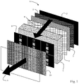
- known LCD stacks such as the LCD stack 1 of Fig. 1 may have a low efficiency, thereby having a high power consumption, whereas it is generally desirable to increase a power efficiency, increase a color gamut, and improve an image contrast.
- each (sub-)pixel waveguide must be manufactured separately in order to distribute RGB laser light to corresponding subpixels, which may lead to a complex system design since for each sub-pixel a corresponding laser must be provided.
- RGB laser diodes may be used as a white light source.
- lasers and LEDs which may be additionally used in the display, may have different emission characteristics.
- a laser may have a smaller light-emitting area and a smaller divergence angle than an LED, such that it may be challenging to ensure uniform illumination without performing adequate diffusion.
- RGB laser diodes may have different efficiencies (e.g. a red diode may have another efficiency than a green diode).
- a GaN based laser diode may be used and for red or green light a VCSEL (vertical cavity surface emitting laser) may be used.
- the light emitted from the one type of laser diodes can be converted into other light by quantum dots, which will be discussed further below.
- color filters may be provided which extract red, green and blue light in order to generate a color by mixing these colors with different strengths.
- the backlight might need to have an unspecific spectrum with a predetermined intensity.
- blue-emitting LEDs with a yellow color-converting phosphor such as Ce:YAG may be present in known devices and color reproducibility may be achieved by narrow passband filters.
- a color purity of the light source may be improved, which has been recognized that it can be achieved with quantum dots.
- some embodiments pertain to a device for a liquid crystal display, including: a light directing portion for guiding light of a first wavelength range from a light source to a plurality of quantum dots, wherein the light directing portion includes a light directing branching; and the plurality of quantum dots configured to emit light of a second wavelength range in response to light of the first wavelength range being incident on a plurality of display elements, each display element including a subset of the plurality of quantum dots, thereby defining a predetermined quantum dot pattern corresponding to the light directing branching.
- a liquid crystal display may be used for displaying images, as it is generally known, and the device according to the present disclosure may be included in the liquid crystal display, thereby replacing at least one component of a known liquid crystal display, as will be described further below.
- the light directing portion may internally reflect the light of the first wavelength range, for example by total reflection, from one end of the light directing portion to another end of the light directing portion.
- the first wavelength range may be blue.
- only blue emitting VCSELs may be used which result in a simpler design than in known devices which may have more laser diodes (e.g. red, green and blue laser diodes).
- the light is decoupled from the light directing portion as an evanescent light wave.
- the light directing portion which may include a plurality of light directing channels in a shape of a light directing branching (which will be discussed further below) is illuminated roughly orthogonal by the light source.
- the light directing portion may have a cuboid shape, such that the largest surface of the cuboid may be illuminated, and the light directing branching may guide the light to one of the smaller surfaces of the cuboid for decoupling the light, or the like.
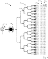
- the light directing portion may include a light directing branching such as one or multiple paths, which, when light enters the light directing portion, distribute the light within the light directing portion.
- the present disclosure is not limited to any material of the light directing portion or any method for providing the light directing branching, although, in some embodiments, the light directing branching is inscribed into a TFT glass with an ultra-short laser pulse technique.
- a micro-structured mirror i.e. a plurality of micro-structured mirrors
- a number of the plurality of micro-structured mirrors may correspond to a number of pixels and/or a number of branches.
- the present disclosure is not limited to that since, depending on an arrangement of the branches, one mirror may be provided which decouples the light from multiple branches.
- the light of the first wavelength range may be directed to the plurality of quantum dots.
- the quantum dots may directly follow (in terms of a light path) after the light directing portion, or it may be envisaged that there is at least one more element between the light directing portion and the plurality of quantum dots.
- quantum dots are known, which are, in some embodiments, semiconductor particles in the nanometer range.
- optical and electronic properties differ between the quantum dots and the larger particles.
- quantum dots In a quantum dot, the motion of electrons and holes is confined by the bandgap structure of the semiconductor materials of which the quantum dot is composed, leading to discrete electronic states.
- quantum dots manufactured by colloidal synthesis have an optically active core and a protective layer formed on the core. The electronic states and, thus, the optical absorption and emission properties (e.g. absorption band, emission profile, emission peaks and corresponding emission wavelengths) can be controlled, in some embodiments, by the size of the core part and the protective layer and their material composition.
- the probability that a certain wavelength is emitted may depend at least on the probability of the corresponding radiative transition of an electron and a hole and, thus, the optical power emitted by the plurality of quantum dots after excitation varies according to the emission profile in some embodiments.
- the emission profile may be understood as the integrated optical power recorded for a plurality of wavelengths in a wavelength range over a certain time interval, wherein the optical power is emitted by a plurality of quantum dots when light of (at least) a predetermined wavelength incident.
- production-related variations for example, in the size of the quantum dots, may contribute to the emission profile and, accordingly, the emission profile may basically reflect an ensemble property of a plurality of quantum dots.
- the emission profile of a material has at least one emission peak which may originate from the lowest radiative electronic state (optically allowed transition) and, as described above for the example of quantum dots, a continuum of wavelengths may be emitted, e.g. an emission peak, and each wavelength may be emitted with a certain probability.
- the emission peak is present at a certain emission wavelength (e.g. a maximum of the peak, a certain wavelength in a wavelength interval characterizing the emission peak such as the full-width-at-half-maximum, or the like), which may correspond to the energy difference between the energy of the radiative state and the ground state (for example energy difference of the electron and hole state).
- the emission wavelength corresponds to the wavelength at which a maximum of the emission peak is present (is recorded).
- Typical materials for manufacturing quantum dots may include InGaAs, CdSe, GaInP, InP, and the like, without limiting the present disclosure in that regard.
- the quantum dots may include multishell quantum dots, such that a high conversion efficiency (i.e. a high quantum yield) may be achieved.
- a multishell quantum dot may be based on a layering of CdSe/CdS/TiO 2 , wherein CdSe may correspond to the active core, CdS may correspond to the protecting layer and TiO 2 may correspond to the dielectric layer.
- a higher efficiency is achieved since a loss (and therefore unused light) within the light directing branching may be considered as close to or equal to zero. Furthermore, the efficiency is increased since only one first wavelength is needed (e.g. due to using blue emitting VCSELs).
- an LCD efficiency is increased due to using polarized (e.g. blue, ultraviolet, etc.) laser light and thus, a polarizer may be omitted. Furthermore, the LCD efficiency is increased due to an omission of a color filter.
- polarized e.g. blue, ultraviolet, etc.
- quantum dots are used according to the present disclosure, a higher color gamut than in known LCDs may be achieved.
- a more cost efficient and thinner LCD stack design may be achieved according to the present disclosure by providing the light directing portion (e.g. by incorporating a laser waveguide (light directing branching) into a TFT glass) and by using quantum dots.
- the light directing portion e.g. by incorporating a laser waveguide (light directing branching) into a TFT glass
- the plurality of quantum dots may be configured to emit light of a second wavelength range in response to an absorption of the light of the first wavelength range.
- the device may include a plurality of display elements (e.g. pixels), wherein each display element may include a subset of the plurality of quantum dots (e.g. two). In such embodiments, not each quantum dot of the plurality of quantum dots may emit light of the second wavelength range.
- each display element may include a subset of the plurality of quantum dots (e.g. two). In such embodiments, not each quantum dot of the plurality of quantum dots may emit light of the second wavelength range.
- a display element may only display one color (of the second wavelength range), or no color at all, if the light of the second wavelength range lies within an infrared or ultraviolet spectrum, or the like.
- each display element includes a quantum dot of a first type configured to emit the light of the second wavelength range and a quantum dot of a second type configured to emit light of a third wavelength range, as discussed herein.
- the present disclosure is not limited to any wavelength or color range, as will be appreciated by the skilled person.
- the second wavelength range may include a yellow color range or a wavelength range which includes several color ranges, infrared light, and/or the like.
- the light directing portion may be adapted to guide the light of the first wavelength range to respective three quantum dots in each display element.
- each display element includes a quantum dot of a first type, configured to emit light of the second wavelength range, a quantum dot of a second type configured to emit light of a third wavelength range and a quantum dot of a third type configured to emit light of a fourth wavelength range.
- the second wavelength range represents a red color range
- the third wavelength range represents a green color range
- the fourth wavelength range represents a blue color range
- each display element is configured to emit the same wavelength ranges.
- a first display element may be configured to emit red and green light only and a second display element may be configured to emit yellow light and blue light (e.g. by letting through blue light, if it is included in the first wavelength range), or the like.
- the light source includes a laser.
- any laser may be envisaged, such as a diode laser, a solid-state laser, a gas laser, a free electron laser, a dye laser, and the like.
- the light directing portion may distribute a laser beam onto each display element, without limiting the present disclosure in that regard.
- more than one laser may be envisaged, wherein the branching of the light directing portion may be adapted accordingly to provide multiple entries for the multiple laser, as may be understood by the person skilled in the art.
- the laser includes a vertical cavity surface emitting laser (VCSEL).
- VCSEL vertical cavity surface emitting laser
- VCSELs are generally known, and may be utilized, in some embodiments, due to their efficiency in providing the first wavelength range, for example.
- VCSELs may be adaptable to a light directing portion according to the present disclosure due to their design, which may allow to couple the light of the first wavelength range into the light directing portion without sacrificing much space of the liquid crystal display.
- a liquid crystal display including: a set of devices for the liquid crystal display, each device including: a light directing portion for guiding light of a first wavelength range from a light source to a plurality of quantum dots, wherein the light directing portion includes a light directing branching; and the plurality of quantum dots configured to emit light of a second wavelength range in response to light of the first wavelength range being incident on a plurality of display elements, each display element including a subset of the plurality of quantum dots, thereby defining a predetermined quantum dot pattern corresponding to the light directing branching.
- each liquid crystal display several devices may be envisaged.
- a 4K resolution of the liquid crystal display may be achieved by including one hundred and twenty-eight devices for the liquid crystal display (and also one hundred and twenty-eight VCSELs, for example).
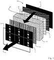
- the liquid crystal display further includes a light directing layer including the set of light directing portions; and a quantum dot layer including the plurality of quantum dots.
- the liquid crystal display may have a layered structure.
- the light directing layer as a first layer
- the quantum dot layer as a second layer.
- additional layers may be envisaged, but not necessarily needed, which will be discussed further below.
- the liquid crystal display may further include a glass layer including the light directing layer.
- the glass layer multiple sub-layers may be included, such as the light directing layer.
- a thin film transistor layer may be included in the glass layer.
- the glass layer further includes a thin film transistor layer.
- Fig. 3 depicts an illustration of a laser inscribing method for manufacturing the light directing portion 20 of Fig. 2 .
- the VCSELs When the VCSELs are distributed both vertical and horizontal sides, they can be distributed equally around the whole display.
- the quantum dot 80 has a thickness of at least or more than thirty-three nanometers.
Landscapes
- Physics & Mathematics (AREA)
- Nonlinear Science (AREA)
- General Physics & Mathematics (AREA)
- Optics & Photonics (AREA)
- Mathematical Physics (AREA)
- Chemical & Material Sciences (AREA)
- Crystallography & Structural Chemistry (AREA)
- Engineering & Computer Science (AREA)
- Microelectronics & Electronic Packaging (AREA)
- Liquid Crystal (AREA)
- Devices For Indicating Variable Information By Combining Individual Elements (AREA)
Applications Claiming Priority (1)
| Application Number | Priority Date | Filing Date | Title |
|---|---|---|---|
| EP21164021 | 2021-03-22 |
Publications (1)
| Publication Number | Publication Date |
|---|---|
| EP4063944A1 true EP4063944A1 (fr) | 2022-09-28 |
Family
ID=75143552
Family Applications (1)
| Application Number | Title | Priority Date | Filing Date |
|---|---|---|---|
| EP22160160.2A Pending EP4063944A1 (fr) | 2021-03-22 | 2022-03-04 | Dispositif pour un affichage à cristaux liquides et affichage à cristaux liquides |
Country Status (2)
| Country | Link |
|---|---|
| US (1) | US12399399B2 (fr) |
| EP (1) | EP4063944A1 (fr) |
Citations (2)
| Publication number | Priority date | Publication date | Assignee | Title |
|---|---|---|---|---|
| US20100053970A1 (en) * | 2008-08-29 | 2010-03-04 | Kabushiki Kaisha Toshiba | Light-emitting device and illuminating device |
| KR20120009740A (ko) * | 2010-07-21 | 2012-02-02 | 엘지디스플레이 주식회사 | 디스플레이 패널 및 이의 제조 방법 |
Family Cites Families (9)
| Publication number | Priority date | Publication date | Assignee | Title |
|---|---|---|---|---|
| JP4850792B2 (ja) * | 2007-07-19 | 2012-01-11 | キヤノン株式会社 | 光変調素子及びそれを有する光変調装置 |
| US8456586B2 (en) * | 2009-06-11 | 2013-06-04 | Apple Inc. | Portable computer display structures |
| EP3540300B1 (fr) * | 2010-11-10 | 2024-05-08 | Shoei Chemical Inc. | Films à points quantiques, dispositifs d'éclairage et procédés d'éclairage |
| TWM540297U (zh) | 2016-09-05 | 2017-04-21 | 揚昇照明股份有限公司 | 背光模組 |
| JPWO2018055766A1 (ja) | 2016-09-26 | 2019-07-04 | 日立化成株式会社 | 硬化性組成物、波長変換材、バックライトユニット、及び画像表示装置 |
| KR102747418B1 (ko) * | 2016-11-28 | 2024-12-27 | 삼성전자주식회사 | 디스플레이장치 |
| US10591774B2 (en) * | 2017-04-10 | 2020-03-17 | Apple Inc. | Displays with collimated light sources and quantum dots |
| ES2967939T3 (es) | 2018-07-26 | 2024-05-06 | Univ Vienna | Emisor de luz de guía de ondas ópticas y pantalla táctil |
| KR102739954B1 (ko) * | 2019-11-20 | 2024-12-09 | 삼성전자주식회사 | 빔 스티어링 장치 및 이를 포함한 시스템 |
-
2022
- 2022-03-04 EP EP22160160.2A patent/EP4063944A1/fr active Pending
- 2022-03-15 US US17/694,705 patent/US12399399B2/en active Active
Patent Citations (2)
| Publication number | Priority date | Publication date | Assignee | Title |
|---|---|---|---|---|
| US20100053970A1 (en) * | 2008-08-29 | 2010-03-04 | Kabushiki Kaisha Toshiba | Light-emitting device and illuminating device |
| KR20120009740A (ko) * | 2010-07-21 | 2012-02-02 | 엘지디스플레이 주식회사 | 디스플레이 패널 및 이의 제조 방법 |
Also Published As
| Publication number | Publication date |
|---|---|
| US12399399B2 (en) | 2025-08-26 |
| US20220299824A1 (en) | 2022-09-22 |
Similar Documents
| Publication | Publication Date | Title |
|---|---|---|
| JP6554593B2 (ja) | 照明装置、表示装置、及びテレビ受信装置 | |
| US7471706B2 (en) | High resolution, full color, high brightness fully integrated light emitting devices and displays | |
| JP6526878B2 (ja) | 照明装置、表示装置及びテレビ受信装置 | |
| US8860907B2 (en) | Backlight unit, liquid crystal display apparatus using the same, and light-emitting diode used therefor | |
| CN107407467B (zh) | 照明装置、显示装置和电视接收装置 | |
| US10656319B2 (en) | Liquid crystal display device | |
| US10762806B2 (en) | Display device | |
| JP2021051965A (ja) | 照明装置及び表示装置 | |
| US10782551B2 (en) | Display device | |
| US10073293B2 (en) | Optical microcavity for a high-contrast display | |
| KR20120056001A (ko) | 백라이트 유닛 및 액정표시장치 | |
| US20200218004A1 (en) | Backlight unit and a display including the same | |
| US20200110309A1 (en) | Lighting device and display device | |
| CN108027119B (zh) | 照明装置、显示装置、电视接收装置及波长转换部的制造方法 | |
| US20240145651A1 (en) | Display device and display | |
| US10175529B2 (en) | Backlight module and liquid crystal display device | |
| US10527770B2 (en) | Light conversion element | |
| US12399399B2 (en) | Device for a liquid crystal display and liquid crystal display | |
| US20180196175A1 (en) | Grating assembly, light source apparatus and driving method of the same | |
| KR20180087487A (ko) | 파장 변환 부재 및 이를 포함하는 백라이트 유닛 | |
| CN116368408B (zh) | 发光基板及其制备方法和发光装置 | |
| CN212517235U (zh) | 显示面板及电子设备 | |
| CN119179216B (zh) | 背光模组和显示装置 | |
| US20190265404A1 (en) | Optical film, backlight module, and display device | |
| KR20200129236A (ko) | 맞춤형 회절격자 도광판을 이용한 고색재현 백라이트 유닛 |
Legal Events
| Date | Code | Title | Description |
|---|---|---|---|
| PUAI | Public reference made under article 153(3) epc to a published international application that has entered the european phase |
Free format text: ORIGINAL CODE: 0009012 |
|
| STAA | Information on the status of an ep patent application or granted ep patent |
Free format text: STATUS: REQUEST FOR EXAMINATION WAS MADE |
|
| 17P | Request for examination filed |
Effective date: 20220307 |
|
| AK | Designated contracting states |
Kind code of ref document: A1 Designated state(s): AL AT BE BG CH CY CZ DE DK EE ES FI FR GB GR HR HU IE IS IT LI LT LU LV MC MK MT NL NO PL PT RO RS SE SI SK SM TR |
|
| STAA | Information on the status of an ep patent application or granted ep patent |
Free format text: STATUS: EXAMINATION IS IN PROGRESS |
|
| 17Q | First examination report despatched |
Effective date: 20250228 |