EP4064254A1 - Elektronische vorrichtung - Google Patents
Elektronische vorrichtung Download PDFInfo
- Publication number
- EP4064254A1 EP4064254A1 EP20889742.1A EP20889742A EP4064254A1 EP 4064254 A1 EP4064254 A1 EP 4064254A1 EP 20889742 A EP20889742 A EP 20889742A EP 4064254 A1 EP4064254 A1 EP 4064254A1
- Authority
- EP
- European Patent Office
- Prior art keywords
- light
- substrate
- passing hole
- shielding layer
- disposed
- Prior art date
- Legal status (The legal status is an assumption and is not a legal conclusion. Google has not performed a legal analysis and makes no representation as to the accuracy of the status listed.)
- Granted
Links
Images
Classifications
-
- H—ELECTRICITY
- H04—ELECTRIC COMMUNICATION TECHNIQUE
- H04N—PICTORIAL COMMUNICATION, e.g. TELEVISION
- H04N23/00—Cameras or camera modules comprising electronic image sensors; Control thereof
-
- G—PHYSICS
- G09—EDUCATION; CRYPTOGRAPHY; DISPLAY; ADVERTISING; SEALS
- G09F—DISPLAYING; ADVERTISING; SIGNS; LABELS OR NAME-PLATES; SEALS
- G09F9/00—Indicating arrangements for variable information in which the information is built-up on a support by selection or combination of individual elements
-
- H—ELECTRICITY
- H04—ELECTRIC COMMUNICATION TECHNIQUE
- H04M—TELEPHONIC COMMUNICATION
- H04M1/00—Substation equipment, e.g. for use by subscribers
- H04M1/02—Constructional features of telephone sets
- H04M1/0202—Portable telephone sets, e.g. cordless phones, mobile phones or bar type handsets
- H04M1/026—Details of the structure or mounting of specific components
- H04M1/0264—Details of the structure or mounting of specific components for a camera module assembly
-
- G—PHYSICS
- G03—PHOTOGRAPHY; CINEMATOGRAPHY; ANALOGOUS TECHNIQUES USING WAVES OTHER THAN OPTICAL WAVES; ELECTROGRAPHY; HOLOGRAPHY
- G03B—APPARATUS OR ARRANGEMENTS FOR TAKING PHOTOGRAPHS OR FOR PROJECTING OR VIEWING THEM; APPARATUS OR ARRANGEMENTS EMPLOYING ANALOGOUS TECHNIQUES USING WAVES OTHER THAN OPTICAL WAVES; ACCESSORIES THEREFOR
- G03B29/00—Combinations of cameras, projectors or photographic printing apparatus with non-photographic non-optical apparatus, e.g. clocks or weapons; Cameras having the shape of other objects
-
- H—ELECTRICITY
- H04—ELECTRIC COMMUNICATION TECHNIQUE
- H04M—TELEPHONIC COMMUNICATION
- H04M1/00—Substation equipment, e.g. for use by subscribers
- H04M1/02—Constructional features of telephone sets
- H04M1/0202—Portable telephone sets, e.g. cordless phones, mobile phones or bar type handsets
- H04M1/026—Details of the structure or mounting of specific components
- H04M1/0266—Details of the structure or mounting of specific components for a display module assembly
-
- H—ELECTRICITY
- H10—SEMICONDUCTOR DEVICES; ELECTRIC SOLID-STATE DEVICES NOT OTHERWISE PROVIDED FOR
- H10K—ORGANIC ELECTRIC SOLID-STATE DEVICES
- H10K59/00—Integrated devices, or assemblies of multiple devices, comprising at least one organic light-emitting element covered by group H10K50/00
- H10K59/80—Constructional details
- H10K59/8791—Arrangements for improving contrast, e.g. preventing reflection of ambient light
- H10K59/8792—Arrangements for improving contrast, e.g. preventing reflection of ambient light comprising light absorbing layers, e.g. black layers
Definitions
- the present disclosure relates to the field of communications device technologies, and in particular, to an electronic device.
- a camera module may be disposed below a display module, and a light-passing hole is disposed on the display module, to ensure that the camera module can work normally.
- the camera module mainly includes components such as a bracket, a lens assembly, and a light shielding layer.
- the lens assembly is mounted in the bracket, the light shielding layer is mounted on the bracket, and the light shielding layer is located above the lens assembly.
- a light-passing hole provided on the display module needs to be greater than an inner diameter of the light shielding layer.
- the present disclosure provides an electronic device, to resolve a problem that a screen-to-body ratio of the electronic device is relatively small.
- An electronic device includes:
- the light shielding layer of the camera module is disposed on a side of the polarizer that is away from the first substrate.
- a distance between the light shielding layer and the display module is approximately zero, so that the first light-passing hole may be smaller.
- there is no assembly error between the display module and the light shielding layer Therefore, the assembly error does not need to be considered when the first light-passing hole is disposed, and a size of the first light-passing hole can be further reduced, so that a screen-to-body ratio of the electronic device is higher.
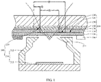
- FIG. 1 is a sectional view of a partial structure of an electronic device disclosed in an embodiment of the present disclosure.
- 100-Display module 110-First substrate, 120-Second substrate, 130-Wiring structure, 140- Light emitting unit, 150-Transparent cover, 160-Optical clear adhesive, 170-Polarizer, 180-Foam, 200-Camera module, 210-Camera body, 211-Light inlet hole, 212-Bracket, 213-Light sensing chip, 220-Light shielding layer.
- an embodiment of the present disclosure discloses an electronic device, and the electronic device may specifically include a display module 100 and a camera module 200.
- the display module 100 may specifically include a first substrate 110, a second substrate 120, and a wiring structure 130.
- the first substrate 110 and the second substrate 120 are stacked, and the wiring structure 130 is disposed on a surface of the second substrate 120 facing the first substrate 110.
- Both the first substrate 110 and the second substrate 120 may be glass plates, and a thin-film transistor may be disposed on the second substrate 120.
- the wiring structure 130 may be an annular structure.
- a first light-passing hole is disposed on the wiring structure 130, and the first light-passing hole may be used for light to pass through, so that light in an external environment can enter the camera module 200.
- the display module 100 may further include a light emitting part 140, a transparent cover 150, an optical clear adhesive 160, a polarizer 170, and a foam 180.
- the light emitting part 140 may be disposed between the first substrate 110 and the second substrate 120, and the light emitting part 140 may be an organic light emitting layer.
- the polarizer 170 may be disposed on a surface of the first substrate 110 facing away from the second substrate 120.
- the transparent cover 150 is located on a side of the first substrate 110 that is away from the second substrate 120, and the transparent cover 150 may be connected to the polarizer 170 by using the optical clear adhesive 160.
- the foam 180 may be disposed on a side of the second substrate 120 that is away from the first substrate 110.
- the foam 180 may be bonded to the second substrate 120, and an avoidance hole may be disposed on the foam 180. At least a part of the camera module 200 may be located in the avoidance hole, to prevent stray light in the display module 100 from affecting normal operation of the camera module 200, and reduce space occupied by the camera module 200, thereby reducing a thickness of the electronic device.
- the camera module 200 specifically includes a camera body 210 and a light shielding layer 220, a light inlet hole 211 is disposed on the camera body 210, the second substrate 120 is located between the first substrate 110 and the camera body 210, the light shielding layer 220 is disposed on a side of the polarizer 170 that is away from the first substrate 110, and a second light-passing hole is disposed on the light shielding layer 220.
- the camera body 210 may specifically include a bracket 212, a lens assembly, and a light sensing chip 213.
- the lens assembly is disposed on the bracket 212, and the lens assembly may include lenses such as a convex lens and a concave lens, to implement effects such as light convergence.
- the light sensing chip 213 may be disposed in the bracket 212.
- the light sensing chip 213 has a light sensing area used for light sensing, and the light sensing chip 213 may convert an optical signal into an electrical signal, to obtain corresponding image information.
- the second light hole herein can also enable light to pass through, so that light in an external environment can enter the camera module 200 and reach the light sensing area of the light sensing chip 213, thereby implementing a shooting function.
- Both the wiring structure 130 and the light shielding layer 220 may play a role of shielding light.
- the first light-passing hole, the second light-passing hole, and the light inlet hole 211 are arranged in an optical axis direction of the camera module 200. Therefore, light in the external environment can successively pass through the second light-passing hole and the first light-passing hole, and finally pass through the light-passing hole 211 to enter the camera module 200, so that the camera module 200 can implement a shooting function.
- Both an orthographic projection of the first light-passing hole on a plane perpendicular to the optical axis direction of the camera module 200 and an orthographic projection of the second light-passing hole on the plane perpendicular to the optical axis direction are within the range of an orthographic projection of the light inlet hole 211 on the plane perpendicular to the optical axis direction.
- both an outline size of the first light-passing hole and an outline size of the second light-passing hole are less than an outline size of the light inlet hole 211.
- a size of the light inlet hole 211 is slightly larger.
- Such setting does not affect a screen-to-body ratio of the display module 100, and it can be ensured that as much light in the external environment enters the camera module 200 as possible.
- the first light-passing hole and the second light-passing hole affect the screen-to-body ratio of the display module 100. Therefore, on a premise that a shooting requirement of the camera module 200 is met, the first light-passing hole and the second light-passing hole may be disposed as small as possible, to reduce occupation rate of a display area by the wiring structure 130 and the light shielding layer 220, thereby improving a screen-to-body ratio of the electronic device.
- the light shielding layer 220 of the camera module 200 is disposed on the display module 100.
- a distance between the light shielding layer 220 and the display module 100 is approximately zero, so that the first light-passing hole may be smaller.
- appearance quality of the electronic device is improved, and user experience is accordingly improved.
- a third light-passing hole is provided on the polarizer 170, and the third light hole may be used to enable light to pass through, to improve light transmittance of an area corresponding to the camera module 200, thereby improving shooting quality of the camera module 200.
- An orthographic projection of the third light-passing hole on the plane perpendicular to the optical axis direction coincides with the orthographic projection of the second light-passing hole on the plane perpendicular to the optical axis direction.
- a part of the optical clear adhesive 160 may extend into the third light-passing hole and the second light-passing hole, to fill the third light-passing hole and the second light-passing hole.
- the part of the optical clear adhesive 160 may be in contact with a surface of the first substrate 110 facing away from the second substrate 120, and is connected to the first substrate 110, so that structural strength of the display module 100 is higher. More importantly, in a process of processing the display module 100, positions of the light shielding layer 220 and the polarizer 170 may refer to each other, so that fast molding of the display module 100 is implemented, and molding efficiency of the display module is improved. In addition, an edge formed after the third light-passing hole is disposed on the polarizer 170 is aligned with an edge formed after the second light-passing hole is disposed on the light shielding layer 220.
- the light shielding layer 220 can be as close to a center line of the third light-passing hole as possible, thereby reducing a size of the light shielding layer 220, so that costs of the light shielding layer 220 are reduced.
- a large size of the light shielding layer 220 can be prevented from increasing a part of the display module 100 that cannot be used for display, thereby improving the screen-to-body ratio of the electronic device.
- the first light-passing hole and the second light-passing hole affect the screen-to-body ratio of the display module 100. Therefore, the first light-passing hole and the second light-passing hole may be disposed as small as possible.
- the orthographic projection of the first light-passing hole on the plane perpendicular to the optical axis direction of the camera module 200 may coincide with the orthographic projection of the second light-passing hole on the plane perpendicular to the optical axis direction.
- a shape of the first light-passing hole is the same as a shape of the second light-passing hole, and sizes of the first light-passing hole and the second light-passing hole are the same.
- both the sizes of the first light-passing hole and the second light-passing hole may be as small as possible.
- relative positions of the first light-passing hole and the second light-passing hole may refer to each other, thereby facilitating processing of the display module 100.
- an outer contour shape of the wiring structure 130 and an outer contour shape of the light shielding layer 220 may be flexibly set.
- the outer contour shape may be rectangular, circular, or oval.
- a shape of the first light-passing hole and a shape of the second light-passing hole may also be flexibly selected, for example, may be a rectangular hole, a circular hole, or an oval hole.
- both the wiring structure 130 and the light shielding layer 220 may be set to annular structures.
- a radial width of the light shielding layer 220 may be less than a radial width of the wiring structure 130, thereby preventing a case in which the radial width of the light shielding layer 220 is excessively large and a light shielding area is excessively large, thereby achieving the foregoing objective.
- H A+D X 2
- H is a size of a hole that cannot be used for display on an external surface of the display module 100
- A is an aperture of the second light-passing hole (or an aperture of the first light-passing hole)
- D is a width of the wiring structure 130.
- A is basically a fixed value
- D is basically a fixed value.
- a size of H is not affected by factors such as an assembly error, and therefore, H may be set to be smaller.
- a distance between a focus of the camera body 210 and the light shielding layer 220 in the optical axis direction may be a preset value.
- a position of the camera body 210 changes, to ensure that a focus of the camera body 210 keeps at a position matching the light shielding layer 220, thereby improving the shooting effect.
- the light shielding layer 220 moves up to the display module 100, a distance between the camera body 210 and the display module 100 can be further reduced, so that distribution of the display module 100 and the camera module 200 is more compact, and therefore, it is more conducive to component stacking in the electronic device.
- the light shielding layer 220 is molded in multiple implementations.
- the light shielding layer 220 may be molded by using a film coating process.
- the light shielding layer 220 may be a film-coated structure. Such a film-coated structure is easy to be molded, and the formed light shielding layer 220 has a relatively small thickness, thereby facilitating control of a thickness of the electronic device.
- the light shielding layer 220 may also be a printed structure.
- the light shielding layer 220 may be formed on a side of the polarizer 170 that is away from the first substrate 110 by using a printing process. This manner also has advantages of being easy to implement and a formed light shielding layer 220 has a relatively small thickness.
- alignment fixing between the light shielding layer 220 and the camera body 210 may be implemented in a manner such as precise positioning of a charge-coupled device (Charge-coupled Device, CCD) camera and dynamic alignment adjustment of a micro motor-driven camera module 200. Therefore, relative position precision of the light shielding layer 220 and the camera body 210 is higher. Therefore, an imaging effect of the camera module 200 is ensured, and a size of the first light-passing hole is increased without considering an alignment error, thereby improving the screen-to-body of the electronic device.
- CCD Charge-coupled Device
- the electronic device disclosed in the embodiments of the present disclosure may be a smartphone, a tablet computer, an e-book reader, or a wearable device.
- the electronic device may also be another device, which is not limited in the embodiments of the present disclosure.
Landscapes
- Engineering & Computer Science (AREA)
- Signal Processing (AREA)
- Physics & Mathematics (AREA)
- General Physics & Mathematics (AREA)
- Theoretical Computer Science (AREA)
- Multimedia (AREA)
- Camera Bodies And Camera Details Or Accessories (AREA)
- Studio Devices (AREA)
Applications Claiming Priority (2)
| Application Number | Priority Date | Filing Date | Title |
|---|---|---|---|
| CN201911129041.XA CN110827672B (zh) | 2019-11-18 | 2019-11-18 | 电子设备 |
| PCT/CN2020/128015 WO2021098565A1 (zh) | 2019-11-18 | 2020-11-11 | 电子设备 |
Publications (3)
| Publication Number | Publication Date |
|---|---|
| EP4064254A1 true EP4064254A1 (de) | 2022-09-28 |
| EP4064254A4 EP4064254A4 (de) | 2023-01-04 |
| EP4064254B1 EP4064254B1 (de) | 2024-08-21 |
Family
ID=69556415
Family Applications (1)
| Application Number | Title | Priority Date | Filing Date |
|---|---|---|---|
| EP20889742.1A Active EP4064254B1 (de) | 2019-11-18 | 2020-11-11 | Elektronische vorrichtung |
Country Status (5)
| Country | Link |
|---|---|
| US (1) | US20220279061A1 (de) |
| EP (1) | EP4064254B1 (de) |
| CN (1) | CN110827672B (de) |
| ES (1) | ES2988073T3 (de) |
| WO (1) | WO2021098565A1 (de) |
Families Citing this family (9)
| Publication number | Priority date | Publication date | Assignee | Title |
|---|---|---|---|---|
| CN110730293B (zh) * | 2019-11-18 | 2021-04-06 | 维沃移动通信有限公司 | 电子设备 |
| CN110827672B (zh) * | 2019-11-18 | 2021-09-21 | 维沃移动通信有限公司 | 电子设备 |
| CN110728905B (zh) | 2019-11-18 | 2021-01-26 | 维沃移动通信有限公司 | 电子设备 |
| CN110784636B (zh) | 2019-11-18 | 2021-03-05 | 维沃移动通信有限公司 | 电子设备 |
| CN113746958B (zh) * | 2020-05-29 | 2022-09-27 | 荣耀终端有限公司 | 电子设备及电子设备的装配方法 |
| CN112615977B (zh) * | 2020-12-02 | 2022-10-18 | 维沃移动通信有限公司 | 电子设备 |
| CN112820197A (zh) * | 2021-02-05 | 2021-05-18 | 维沃移动通信有限公司 | 电子设备、显示屏及显示屏的制备方法 |
| CN113013219B (zh) * | 2021-03-11 | 2024-02-02 | 武汉华星光电半导体显示技术有限公司 | 显示装置 |
| CN113539067B (zh) * | 2021-06-22 | 2022-10-28 | 云谷(固安)科技有限公司 | 一种屏体组件 |
Family Cites Families (26)
| Publication number | Priority date | Publication date | Assignee | Title |
|---|---|---|---|---|
| JP2007116361A (ja) * | 2005-10-19 | 2007-05-10 | Sony Ericsson Mobilecommunications Japan Inc | カメラ付き携帯端末及び撮像装置 |
| US8509864B1 (en) * | 2010-07-16 | 2013-08-13 | Incase Designs Corp. | Preventing glare to camera from flash in smartphone case |
| JP5773275B2 (ja) * | 2012-04-27 | 2015-09-02 | 大日本印刷株式会社 | 通知窓付き表示装置用前面保護板、及び表示装置 |
| US10191577B2 (en) * | 2016-02-16 | 2019-01-29 | Samsung Electronics Co., Ltd. | Electronic device |
| CN207720201U (zh) * | 2017-12-13 | 2018-08-10 | 维沃移动通信有限公司 | 一种移动终端 |
| WO2019210728A1 (en) * | 2018-05-04 | 2019-11-07 | Guangdong Oppo Mobile Telecommunications Corp., Ltd. | Mobile terminal |
| CN108769313B (zh) * | 2018-05-29 | 2021-05-25 | 维沃移动通信有限公司 | 一种移动终端 |
| CN108845450B (zh) * | 2018-06-29 | 2021-06-04 | Oppo广东移动通信有限公司 | 显示组件和电子设备 |
| CN108957829A (zh) * | 2018-07-06 | 2018-12-07 | Oppo广东移动通信有限公司 | 显示屏组件、电子设备及电子设备的制作方法 |
| CN108957819A (zh) * | 2018-07-09 | 2018-12-07 | Oppo广东移动通信有限公司 | 电子装置 |
| CN108681131B (zh) * | 2018-07-27 | 2021-07-30 | 厦门天马微电子有限公司 | 显示装置 |
| CN209267626U (zh) * | 2018-12-26 | 2019-08-16 | 维沃移动通信有限公司 | 终端设备 |
| CN209266408U (zh) * | 2019-01-16 | 2019-08-16 | 信利光电股份有限公司 | 一种显示屏及触摸显示模组 |
| CN209460528U (zh) * | 2019-03-27 | 2019-10-01 | 信利光电股份有限公司 | 一种显示装置 |
| CN110049161B (zh) * | 2019-05-06 | 2021-01-15 | 维沃移动通信有限公司 | 移动终端 |
| CN110049223B (zh) * | 2019-05-08 | 2021-09-03 | 维沃移动通信有限公司 | 一种摄像头组件及移动终端 |
| CN110062082B (zh) * | 2019-05-24 | 2024-05-17 | Oppo广东移动通信有限公司 | 一种显示屏及终端设备 |
| CN110120996B (zh) * | 2019-06-06 | 2021-04-27 | Oppo广东移动通信有限公司 | Oled通孔屏、移动终端、摄像控制方法、装置及存储介质 |
| CN209608699U (zh) * | 2019-06-10 | 2019-11-08 | Oppo广东移动通信有限公司 | 移动终端及其显示屏 |
| CN110300246B (zh) * | 2019-06-28 | 2024-10-15 | Oppo广东移动通信有限公司 | 电子设备 |
| CN110335890A (zh) * | 2019-07-11 | 2019-10-15 | 京东方科技集团股份有限公司 | 一种显示面板及其制备方法、显示装置 |
| CN110426878A (zh) * | 2019-07-16 | 2019-11-08 | 武汉华星光电技术有限公司 | 显示装置 |
| CN110827672B (zh) * | 2019-11-18 | 2021-09-21 | 维沃移动通信有限公司 | 电子设备 |
| CN110784635B (zh) * | 2019-11-18 | 2021-05-18 | 维沃移动通信有限公司 | 电子设备 |
| CN110730293B (zh) * | 2019-11-18 | 2021-04-06 | 维沃移动通信有限公司 | 电子设备 |
| CN110784636B (zh) * | 2019-11-18 | 2021-03-05 | 维沃移动通信有限公司 | 电子设备 |
-
2019
- 2019-11-18 CN CN201911129041.XA patent/CN110827672B/zh active Active
-
2020
- 2020-11-11 ES ES20889742T patent/ES2988073T3/es active Active
- 2020-11-11 EP EP20889742.1A patent/EP4064254B1/de active Active
- 2020-11-11 WO PCT/CN2020/128015 patent/WO2021098565A1/zh not_active Ceased
-
2022
- 2022-05-17 US US17/746,907 patent/US20220279061A1/en active Pending
Also Published As
| Publication number | Publication date |
|---|---|
| US20220279061A1 (en) | 2022-09-01 |
| CN110827672B (zh) | 2021-09-21 |
| CN110827672A (zh) | 2020-02-21 |
| EP4064254A4 (de) | 2023-01-04 |
| ES2988073T3 (es) | 2024-11-19 |
| WO2021098565A1 (zh) | 2021-05-27 |
| EP4064254B1 (de) | 2024-08-21 |
Similar Documents
| Publication | Publication Date | Title |
|---|---|---|
| US20220279061A1 (en) | Electronic device | |
| US12069360B2 (en) | Electronic device | |
| US11968438B2 (en) | Electronic device | |
| US20220279104A1 (en) | Electronic device | |
| CN205333947U (zh) | 成像镜头模块及电子装置 | |
| CN110730293B (zh) | 电子设备 | |
| CN109425917B (zh) | 塑胶透镜、塑胶环形光学元件、镜头模块及电子装置 | |
| CN209728594U (zh) | 显示模组及终端设备 | |
| CN107357025A (zh) | 成像镜头及电子装置 | |
| JP2017090875A (ja) | レンズモジュール | |
| EP4006609A1 (de) | Fotografieranordnung unter dem bildschirm, fotografiermodul, optische kamera und herstellungsverfahren für das fotomodul und die optische kamera | |
| CN109831603B (zh) | 移动终端 | |
| US20200057237A1 (en) | Lens module | |
| CN110312012A (zh) | 电子设备 | |
| CN211266962U (zh) | 金属遮光件、摄像模组及电子设备 | |
| CN211263915U (zh) | 一种成像镜头及电子装置 | |
| TWI691782B (zh) | 塑膠鏡筒、成像鏡頭模組及電子裝置 | |
| CN209964149U (zh) | 电子设备 | |
| CN207867192U (zh) | 镜头模组 | |
| CN210327670U (zh) | 电子设备 | |
| CN210429124U (zh) | 电子设备 | |
| CN113777734A (zh) | 镜头组件、镜头模块及电子装置 | |
| WO2025000465A1 (zh) | 镜头装置及电子设备 |
Legal Events
| Date | Code | Title | Description |
|---|---|---|---|
| STAA | Information on the status of an ep patent application or granted ep patent |
Free format text: STATUS: THE INTERNATIONAL PUBLICATION HAS BEEN MADE |
|
| PUAI | Public reference made under article 153(3) epc to a published international application that has entered the european phase |
Free format text: ORIGINAL CODE: 0009012 |
|
| STAA | Information on the status of an ep patent application or granted ep patent |
Free format text: STATUS: REQUEST FOR EXAMINATION WAS MADE |
|
| 17P | Request for examination filed |
Effective date: 20220614 |
|
| AK | Designated contracting states |
Kind code of ref document: A1 Designated state(s): AL AT BE BG CH CY CZ DE DK EE ES FI FR GB GR HR HU IE IS IT LI LT LU LV MC MK MT NL NO PL PT RO RS SE SI SK SM TR |
|
| REG | Reference to a national code |
Ref country code: DE Ref legal event code: R079 Free format text: PREVIOUS MAIN CLASS: G09F0009000000 Ipc: H04M0001020000 Ref country code: DE Ref legal event code: R079 Ref document number: 602020036427 Country of ref document: DE Free format text: PREVIOUS MAIN CLASS: G09F0009000000 Ipc: H04M0001020000 |
|
| A4 | Supplementary search report drawn up and despatched |
Effective date: 20221202 |
|
| RIC1 | Information provided on ipc code assigned before grant |
Ipc: H04M 1/02 20060101AFI20221128BHEP |
|
| DAV | Request for validation of the european patent (deleted) | ||
| DAX | Request for extension of the european patent (deleted) | ||
| GRAP | Despatch of communication of intention to grant a patent |
Free format text: ORIGINAL CODE: EPIDOSNIGR1 |
|
| STAA | Information on the status of an ep patent application or granted ep patent |
Free format text: STATUS: GRANT OF PATENT IS INTENDED |
|
| INTG | Intention to grant announced |
Effective date: 20240325 |
|
| GRAS | Grant fee paid |
Free format text: ORIGINAL CODE: EPIDOSNIGR3 |
|
| GRAA | (expected) grant |
Free format text: ORIGINAL CODE: 0009210 |
|
| STAA | Information on the status of an ep patent application or granted ep patent |
Free format text: STATUS: THE PATENT HAS BEEN GRANTED |
|
| AK | Designated contracting states |
Kind code of ref document: B1 Designated state(s): AL AT BE BG CH CY CZ DE DK EE ES FI FR GB GR HR HU IE IS IT LI LT LU LV MC MK MT NL NO PL PT RO RS SE SI SK SM TR |
|
| REG | Reference to a national code |
Ref country code: GB Ref legal event code: FG4D |
|
| REG | Reference to a national code |
Ref country code: CH Ref legal event code: EP |
|
| REG | Reference to a national code |
Ref country code: DE Ref legal event code: R096 Ref document number: 602020036427 Country of ref document: DE |
|
| REG | Reference to a national code |
Ref country code: IE Ref legal event code: FG4D |
|
| REG | Reference to a national code |
Ref country code: NL Ref legal event code: FP |
|
| REG | Reference to a national code |
Ref country code: ES Ref legal event code: FG2A Ref document number: 2988073 Country of ref document: ES Kind code of ref document: T3 Effective date: 20241119 |
|
| REG | Reference to a national code |
Ref country code: LT Ref legal event code: MG9D |
|
| PG25 | Lapsed in a contracting state [announced via postgrant information from national office to epo] |
Ref country code: NO Free format text: LAPSE BECAUSE OF FAILURE TO SUBMIT A TRANSLATION OF THE DESCRIPTION OR TO PAY THE FEE WITHIN THE PRESCRIBED TIME-LIMIT Effective date: 20241121 |
|
| REG | Reference to a national code |
Ref country code: AT Ref legal event code: MK05 Ref document number: 1716695 Country of ref document: AT Kind code of ref document: T Effective date: 20240821 |
|
| PG25 | Lapsed in a contracting state [announced via postgrant information from national office to epo] |
Ref country code: PT Free format text: LAPSE BECAUSE OF FAILURE TO SUBMIT A TRANSLATION OF THE DESCRIPTION OR TO PAY THE FEE WITHIN THE PRESCRIBED TIME-LIMIT Effective date: 20241223 Ref country code: PL Free format text: LAPSE BECAUSE OF FAILURE TO SUBMIT A TRANSLATION OF THE DESCRIPTION OR TO PAY THE FEE WITHIN THE PRESCRIBED TIME-LIMIT Effective date: 20240821 Ref country code: GR Free format text: LAPSE BECAUSE OF FAILURE TO SUBMIT A TRANSLATION OF THE DESCRIPTION OR TO PAY THE FEE WITHIN THE PRESCRIBED TIME-LIMIT Effective date: 20241122 Ref country code: FI Free format text: LAPSE BECAUSE OF FAILURE TO SUBMIT A TRANSLATION OF THE DESCRIPTION OR TO PAY THE FEE WITHIN THE PRESCRIBED TIME-LIMIT Effective date: 20240821 |
|
| PG25 | Lapsed in a contracting state [announced via postgrant information from national office to epo] |
Ref country code: BG Free format text: LAPSE BECAUSE OF FAILURE TO SUBMIT A TRANSLATION OF THE DESCRIPTION OR TO PAY THE FEE WITHIN THE PRESCRIBED TIME-LIMIT Effective date: 20240821 |
|
| PG25 | Lapsed in a contracting state [announced via postgrant information from national office to epo] |
Ref country code: LV Free format text: LAPSE BECAUSE OF FAILURE TO SUBMIT A TRANSLATION OF THE DESCRIPTION OR TO PAY THE FEE WITHIN THE PRESCRIBED TIME-LIMIT Effective date: 20240821 |
|
| PG25 | Lapsed in a contracting state [announced via postgrant information from national office to epo] |
Ref country code: AT Free format text: LAPSE BECAUSE OF FAILURE TO SUBMIT A TRANSLATION OF THE DESCRIPTION OR TO PAY THE FEE WITHIN THE PRESCRIBED TIME-LIMIT Effective date: 20240821 Ref country code: IS Free format text: LAPSE BECAUSE OF FAILURE TO SUBMIT A TRANSLATION OF THE DESCRIPTION OR TO PAY THE FEE WITHIN THE PRESCRIBED TIME-LIMIT Effective date: 20241221 |
|
| PG25 | Lapsed in a contracting state [announced via postgrant information from national office to epo] |
Ref country code: HR Free format text: LAPSE BECAUSE OF FAILURE TO SUBMIT A TRANSLATION OF THE DESCRIPTION OR TO PAY THE FEE WITHIN THE PRESCRIBED TIME-LIMIT Effective date: 20240821 |
|
| PG25 | Lapsed in a contracting state [announced via postgrant information from national office to epo] |
Ref country code: RS Free format text: LAPSE BECAUSE OF FAILURE TO SUBMIT A TRANSLATION OF THE DESCRIPTION OR TO PAY THE FEE WITHIN THE PRESCRIBED TIME-LIMIT Effective date: 20241121 |
|
| PG25 | Lapsed in a contracting state [announced via postgrant information from national office to epo] |
Ref country code: RS Free format text: LAPSE BECAUSE OF FAILURE TO SUBMIT A TRANSLATION OF THE DESCRIPTION OR TO PAY THE FEE WITHIN THE PRESCRIBED TIME-LIMIT Effective date: 20241121 Ref country code: PT Free format text: LAPSE BECAUSE OF FAILURE TO SUBMIT A TRANSLATION OF THE DESCRIPTION OR TO PAY THE FEE WITHIN THE PRESCRIBED TIME-LIMIT Effective date: 20241223 Ref country code: PL Free format text: LAPSE BECAUSE OF FAILURE TO SUBMIT A TRANSLATION OF THE DESCRIPTION OR TO PAY THE FEE WITHIN THE PRESCRIBED TIME-LIMIT Effective date: 20240821 Ref country code: NO Free format text: LAPSE BECAUSE OF FAILURE TO SUBMIT A TRANSLATION OF THE DESCRIPTION OR TO PAY THE FEE WITHIN THE PRESCRIBED TIME-LIMIT Effective date: 20241121 Ref country code: LV Free format text: LAPSE BECAUSE OF FAILURE TO SUBMIT A TRANSLATION OF THE DESCRIPTION OR TO PAY THE FEE WITHIN THE PRESCRIBED TIME-LIMIT Effective date: 20240821 Ref country code: IS Free format text: LAPSE BECAUSE OF FAILURE TO SUBMIT A TRANSLATION OF THE DESCRIPTION OR TO PAY THE FEE WITHIN THE PRESCRIBED TIME-LIMIT Effective date: 20241221 Ref country code: HR Free format text: LAPSE BECAUSE OF FAILURE TO SUBMIT A TRANSLATION OF THE DESCRIPTION OR TO PAY THE FEE WITHIN THE PRESCRIBED TIME-LIMIT Effective date: 20240821 Ref country code: GR Free format text: LAPSE BECAUSE OF FAILURE TO SUBMIT A TRANSLATION OF THE DESCRIPTION OR TO PAY THE FEE WITHIN THE PRESCRIBED TIME-LIMIT Effective date: 20241122 Ref country code: FI Free format text: LAPSE BECAUSE OF FAILURE TO SUBMIT A TRANSLATION OF THE DESCRIPTION OR TO PAY THE FEE WITHIN THE PRESCRIBED TIME-LIMIT Effective date: 20240821 Ref country code: BG Free format text: LAPSE BECAUSE OF FAILURE TO SUBMIT A TRANSLATION OF THE DESCRIPTION OR TO PAY THE FEE WITHIN THE PRESCRIBED TIME-LIMIT Effective date: 20240821 Ref country code: AT Free format text: LAPSE BECAUSE OF FAILURE TO SUBMIT A TRANSLATION OF THE DESCRIPTION OR TO PAY THE FEE WITHIN THE PRESCRIBED TIME-LIMIT Effective date: 20240821 |
|
| PG25 | Lapsed in a contracting state [announced via postgrant information from national office to epo] |
Ref country code: SM Free format text: LAPSE BECAUSE OF FAILURE TO SUBMIT A TRANSLATION OF THE DESCRIPTION OR TO PAY THE FEE WITHIN THE PRESCRIBED TIME-LIMIT Effective date: 20240821 Ref country code: RO Free format text: LAPSE BECAUSE OF FAILURE TO SUBMIT A TRANSLATION OF THE DESCRIPTION OR TO PAY THE FEE WITHIN THE PRESCRIBED TIME-LIMIT Effective date: 20240821 Ref country code: DK Free format text: LAPSE BECAUSE OF FAILURE TO SUBMIT A TRANSLATION OF THE DESCRIPTION OR TO PAY THE FEE WITHIN THE PRESCRIBED TIME-LIMIT Effective date: 20240821 |
|
| PG25 | Lapsed in a contracting state [announced via postgrant information from national office to epo] |
Ref country code: EE Free format text: LAPSE BECAUSE OF FAILURE TO SUBMIT A TRANSLATION OF THE DESCRIPTION OR TO PAY THE FEE WITHIN THE PRESCRIBED TIME-LIMIT Effective date: 20240821 |
|
| PG25 | Lapsed in a contracting state [announced via postgrant information from national office to epo] |
Ref country code: CZ Free format text: LAPSE BECAUSE OF FAILURE TO SUBMIT A TRANSLATION OF THE DESCRIPTION OR TO PAY THE FEE WITHIN THE PRESCRIBED TIME-LIMIT Effective date: 20240821 |
|
| PG25 | Lapsed in a contracting state [announced via postgrant information from national office to epo] |
Ref country code: SK Free format text: LAPSE BECAUSE OF FAILURE TO SUBMIT A TRANSLATION OF THE DESCRIPTION OR TO PAY THE FEE WITHIN THE PRESCRIBED TIME-LIMIT Effective date: 20240821 |
|
| REG | Reference to a national code |
Ref country code: DE Ref legal event code: R097 Ref document number: 602020036427 Country of ref document: DE |
|
| PLBE | No opposition filed within time limit |
Free format text: ORIGINAL CODE: 0009261 |
|
| STAA | Information on the status of an ep patent application or granted ep patent |
Free format text: STATUS: NO OPPOSITION FILED WITHIN TIME LIMIT |
|
| REG | Reference to a national code |
Ref country code: CH Ref legal event code: PL |
|
| PG25 | Lapsed in a contracting state [announced via postgrant information from national office to epo] |
Ref country code: MC Free format text: LAPSE BECAUSE OF FAILURE TO SUBMIT A TRANSLATION OF THE DESCRIPTION OR TO PAY THE FEE WITHIN THE PRESCRIBED TIME-LIMIT Effective date: 20240821 |
|
| PG25 | Lapsed in a contracting state [announced via postgrant information from national office to epo] |
Ref country code: LU Free format text: LAPSE BECAUSE OF NON-PAYMENT OF DUE FEES Effective date: 20241111 |
|
| REG | Reference to a national code |
Ref country code: CH Ref legal event code: PL |
|
| PG25 | Lapsed in a contracting state [announced via postgrant information from national office to epo] |
Ref country code: CH Free format text: LAPSE BECAUSE OF NON-PAYMENT OF DUE FEES Effective date: 20241130 |
|
| 26N | No opposition filed |
Effective date: 20250522 |
|
| REG | Reference to a national code |
Ref country code: BE Ref legal event code: MM Effective date: 20241130 |
|
| PG25 | Lapsed in a contracting state [announced via postgrant information from national office to epo] |
Ref country code: SE Free format text: LAPSE BECAUSE OF FAILURE TO SUBMIT A TRANSLATION OF THE DESCRIPTION OR TO PAY THE FEE WITHIN THE PRESCRIBED TIME-LIMIT Effective date: 20240821 |
|
| PG25 | Lapsed in a contracting state [announced via postgrant information from national office to epo] |
Ref country code: BE Free format text: LAPSE BECAUSE OF NON-PAYMENT OF DUE FEES Effective date: 20241130 |
|
| PGFP | Annual fee paid to national office [announced via postgrant information from national office to epo] |
Ref country code: FR Payment date: 20250930 Year of fee payment: 6 |
|
| PG25 | Lapsed in a contracting state [announced via postgrant information from national office to epo] |
Ref country code: IE Free format text: LAPSE BECAUSE OF NON-PAYMENT OF DUE FEES Effective date: 20241111 |
|
| PGFP | Annual fee paid to national office [announced via postgrant information from national office to epo] |
Ref country code: NL Payment date: 20251003 Year of fee payment: 6 |
|
| PGFP | Annual fee paid to national office [announced via postgrant information from national office to epo] |
Ref country code: DE Payment date: 20250930 Year of fee payment: 6 |
|
| PGFP | Annual fee paid to national office [announced via postgrant information from national office to epo] |
Ref country code: GB Payment date: 20251001 Year of fee payment: 6 |
|
| PGFP | Annual fee paid to national office [announced via postgrant information from national office to epo] |
Ref country code: IT Payment date: 20251022 Year of fee payment: 6 |
|
| PGFP | Annual fee paid to national office [announced via postgrant information from national office to epo] |
Ref country code: ES Payment date: 20251211 Year of fee payment: 6 |
|
| PG25 | Lapsed in a contracting state [announced via postgrant information from national office to epo] |
Ref country code: HU Free format text: LAPSE BECAUSE OF FAILURE TO SUBMIT A TRANSLATION OF THE DESCRIPTION OR TO PAY THE FEE WITHIN THE PRESCRIBED TIME-LIMIT; INVALID AB INITIO Effective date: 20201111 |
|
| PG25 | Lapsed in a contracting state [announced via postgrant information from national office to epo] |
Ref country code: CY Free format text: LAPSE BECAUSE OF FAILURE TO SUBMIT A TRANSLATION OF THE DESCRIPTION OR TO PAY THE FEE WITHIN THE PRESCRIBED TIME-LIMIT; INVALID AB INITIO Effective date: 20201111 |