EP4064364A1 - Dispositif à semi-conducteur comprenant une structure de tranchée - Google Patents
Dispositif à semi-conducteur comprenant une structure de tranchée Download PDFInfo
- Publication number
- EP4064364A1 EP4064364A1 EP21164244.2A EP21164244A EP4064364A1 EP 4064364 A1 EP4064364 A1 EP 4064364A1 EP 21164244 A EP21164244 A EP 21164244A EP 4064364 A1 EP4064364 A1 EP 4064364A1
- Authority
- EP
- European Patent Office
- Prior art keywords
- trench
- semiconductor device
- gap
- dielectric
- electrode
- Prior art date
- Legal status (The legal status is an assumption and is not a legal conclusion. Google has not performed a legal analysis and makes no representation as to the accuracy of the status listed.)
- Pending
Links
Images

Classifications
-
- H—ELECTRICITY
- H10—SEMICONDUCTOR DEVICES; ELECTRIC SOLID-STATE DEVICES NOT OTHERWISE PROVIDED FOR
- H10D—INORGANIC ELECTRIC SEMICONDUCTOR DEVICES
- H10D64/00—Electrodes of devices having potential barriers
- H10D64/111—Field plates
- H10D64/117—Recessed field plates, e.g. trench field plates or buried field plates
-
- H—ELECTRICITY
- H10—SEMICONDUCTOR DEVICES; ELECTRIC SOLID-STATE DEVICES NOT OTHERWISE PROVIDED FOR
- H10D—INORGANIC ELECTRIC SEMICONDUCTOR DEVICES
- H10D64/00—Electrodes of devices having potential barriers
- H10D64/20—Electrodes characterised by their shapes, relative sizes or dispositions
- H10D64/27—Electrodes not carrying the current to be rectified, amplified, oscillated or switched, e.g. gates
- H10D64/311—Gate electrodes for field-effect devices
- H10D64/411—Gate electrodes for field-effect devices for FETs
- H10D64/511—Gate electrodes for field-effect devices for FETs for IGFETs
- H10D64/512—Disposition of the gate electrodes, e.g. buried gates
- H10D64/513—Disposition of the gate electrodes, e.g. buried gates within recesses in the substrate, e.g. trench gates, groove gates or buried gates
-
- H—ELECTRICITY
- H10—SEMICONDUCTOR DEVICES; ELECTRIC SOLID-STATE DEVICES NOT OTHERWISE PROVIDED FOR
- H10D—INORGANIC ELECTRIC SEMICONDUCTOR DEVICES
- H10D12/00—Bipolar devices controlled by the field effect, e.g. insulated-gate bipolar transistors [IGBT]
- H10D12/411—Insulated-gate bipolar transistors [IGBT]
- H10D12/441—Vertical IGBTs
- H10D12/461—Vertical IGBTs having non-planar surfaces, e.g. having trenches, recesses or pillars in the surfaces of the emitter, base or collector regions
- H10D12/481—Vertical IGBTs having non-planar surfaces, e.g. having trenches, recesses or pillars in the surfaces of the emitter, base or collector regions having gate structures on slanted surfaces, on vertical surfaces, or in grooves, e.g. trench gate IGBTs
-
- H—ELECTRICITY
- H10—SEMICONDUCTOR DEVICES; ELECTRIC SOLID-STATE DEVICES NOT OTHERWISE PROVIDED FOR
- H10D—INORGANIC ELECTRIC SEMICONDUCTOR DEVICES
- H10D30/00—Field-effect transistors [FET]
- H10D30/60—Insulated-gate field-effect transistors [IGFET]
- H10D30/64—Double-diffused metal-oxide semiconductor [DMOS] FETs
- H10D30/66—Vertical DMOS [VDMOS] FETs
- H10D30/668—Vertical DMOS [VDMOS] FETs having trench gate electrodes, e.g. UMOS transistors
-
- H—ELECTRICITY
- H10—SEMICONDUCTOR DEVICES; ELECTRIC SOLID-STATE DEVICES NOT OTHERWISE PROVIDED FOR
- H10D—INORGANIC ELECTRIC SEMICONDUCTOR DEVICES
- H10D62/00—Semiconductor bodies, or regions thereof, of devices having potential barriers
- H10D62/10—Shapes, relative sizes or dispositions of the regions of the semiconductor bodies; Shapes of the semiconductor bodies
- H10D62/113—Isolations within a component, i.e. internal isolations
- H10D62/115—Dielectric isolations, e.g. air gaps
-
- H—ELECTRICITY
- H10—SEMICONDUCTOR DEVICES; ELECTRIC SOLID-STATE DEVICES NOT OTHERWISE PROVIDED FOR
- H10D—INORGANIC ELECTRIC SEMICONDUCTOR DEVICES
- H10D64/00—Electrodes of devices having potential barriers
- H10D64/111—Field plates
- H10D64/112—Field plates comprising multiple field plate segments
-
- H—ELECTRICITY
- H10—SEMICONDUCTOR DEVICES; ELECTRIC SOLID-STATE DEVICES NOT OTHERWISE PROVIDED FOR
- H10D—INORGANIC ELECTRIC SEMICONDUCTOR DEVICES
- H10D64/00—Electrodes of devices having potential barriers
- H10D64/20—Electrodes characterised by their shapes, relative sizes or dispositions
-
- H—ELECTRICITY
- H10—SEMICONDUCTOR DEVICES; ELECTRIC SOLID-STATE DEVICES NOT OTHERWISE PROVIDED FOR
- H10D—INORGANIC ELECTRIC SEMICONDUCTOR DEVICES
- H10D64/00—Electrodes of devices having potential barriers
- H10D64/20—Electrodes characterised by their shapes, relative sizes or dispositions
- H10D64/27—Electrodes not carrying the current to be rectified, amplified, oscillated or switched, e.g. gates
- H10D64/311—Gate electrodes for field-effect devices
- H10D64/411—Gate electrodes for field-effect devices for FETs
- H10D64/511—Gate electrodes for field-effect devices for FETs for IGFETs
- H10D64/514—Gate electrodes for field-effect devices for FETs for IGFETs characterised by the insulating layers
- H10D64/516—Gate electrodes for field-effect devices for FETs for IGFETs characterised by the insulating layers the thicknesses being non-uniform
-
- H—ELECTRICITY
- H10—SEMICONDUCTOR DEVICES; ELECTRIC SOLID-STATE DEVICES NOT OTHERWISE PROVIDED FOR
- H10D—INORGANIC ELECTRIC SEMICONDUCTOR DEVICES
- H10D64/00—Electrodes of devices having potential barriers
- H10D64/20—Electrodes characterised by their shapes, relative sizes or dispositions
- H10D64/27—Electrodes not carrying the current to be rectified, amplified, oscillated or switched, e.g. gates
- H10D64/311—Gate electrodes for field-effect devices
- H10D64/411—Gate electrodes for field-effect devices for FETs
- H10D64/511—Gate electrodes for field-effect devices for FETs for IGFETs
- H10D64/517—Gate electrodes for field-effect devices for FETs for IGFETs characterised by the conducting layers
- H10D64/518—Gate electrodes for field-effect devices for FETs for IGFETs characterised by the conducting layers characterised by their lengths or sectional shapes
-
- H—ELECTRICITY
- H10—SEMICONDUCTOR DEVICES; ELECTRIC SOLID-STATE DEVICES NOT OTHERWISE PROVIDED FOR
- H10D—INORGANIC ELECTRIC SEMICONDUCTOR DEVICES
- H10D64/00—Electrodes of devices having potential barriers
- H10D64/60—Electrodes characterised by their materials
- H10D64/66—Electrodes having a conductor capacitively coupled to a semiconductor by an insulator, e.g. MIS electrodes
- H10D64/675—Gate sidewall spacers
- H10D64/679—Gate sidewall spacers comprising air gaps
-
- H—ELECTRICITY
- H10—SEMICONDUCTOR DEVICES; ELECTRIC SOLID-STATE DEVICES NOT OTHERWISE PROVIDED FOR
- H10D—INORGANIC ELECTRIC SEMICONDUCTOR DEVICES
- H10D64/00—Electrodes of devices having potential barriers
- H10D64/60—Electrodes characterised by their materials
- H10D64/66—Electrodes having a conductor capacitively coupled to a semiconductor by an insulator, e.g. MIS electrodes
- H10D64/68—Electrodes having a conductor capacitively coupled to a semiconductor by an insulator, e.g. MIS electrodes characterised by the insulator, e.g. by the gate insulator
- H10D64/687—Electrodes having a conductor capacitively coupled to a semiconductor by an insulator, e.g. MIS electrodes characterised by the insulator, e.g. by the gate insulator having cavities, e.g. porous gate dielectrics having gasses therein
-
- H—ELECTRICITY
- H10—SEMICONDUCTOR DEVICES; ELECTRIC SOLID-STATE DEVICES NOT OTHERWISE PROVIDED FOR
- H10D—INORGANIC ELECTRIC SEMICONDUCTOR DEVICES
- H10D62/00—Semiconductor bodies, or regions thereof, of devices having potential barriers
- H10D62/80—Semiconductor bodies, or regions thereof, of devices having potential barriers characterised by the materials
- H10D62/83—Semiconductor bodies, or regions thereof, of devices having potential barriers characterised by the materials being Group IV materials, e.g. B-doped Si or undoped Ge
- H10D62/832—Semiconductor bodies, or regions thereof, of devices having potential barriers characterised by the materials being Group IV materials, e.g. B-doped Si or undoped Ge being Group IV materials comprising two or more elements, e.g. SiGe
- H10D62/8325—Silicon carbide
-
- H—ELECTRICITY
- H10—SEMICONDUCTOR DEVICES; ELECTRIC SOLID-STATE DEVICES NOT OTHERWISE PROVIDED FOR
- H10D—INORGANIC ELECTRIC SEMICONDUCTOR DEVICES
- H10D64/00—Electrodes of devices having potential barriers
- H10D64/20—Electrodes characterised by their shapes, relative sizes or dispositions
- H10D64/23—Electrodes carrying the current to be rectified, amplified, oscillated or switched, e.g. sources, drains, anodes or cathodes
- H10D64/251—Source or drain electrodes for field-effect devices
- H10D64/252—Source or drain electrodes for field-effect devices for vertical or pseudo-vertical devices
- H10D64/2527—Source or drain electrodes for field-effect devices for vertical or pseudo-vertical devices for vertical devices wherein the source or drain electrodes are recessed in semiconductor bodies
Definitions
- the present disclosure is related to a semiconductor device, in particular to a semiconductor device including a trench structure.
- IGFETs insulated gate field effect transistors
- MOSFETs metal oxide semiconductor field effect transistors
- IGBTs insulated gate bipolar transistors
- shrinking device geometries a variety of tradeoffs and challenges have to be met when increasing device functionalities per unit area.
- shrinking of device geometries may be accompanied by challenges for meeting demands on device reliability that may be caused by high electric fields in trench dielectrics.
- the semiconductor device includes a semiconductor body having a first main surface.
- the semiconductor device further includes a trench structure extending into the semiconductor body from the first main surface.
- the trench structure further includes a trench electrode structure and a trench dielectric structure.
- the trench dielectric structure includes a gate dielectric in an upper part of the trench dielectric structure and a gap in a lower part of the trench dielectric structure.
- the semiconductor device further includes a body region adjoining the gate dielectric at a sidewall of the trench structure in the upper part of the trench dielectric structure. The gate dielectric extends deeper into the semiconductor body along the sidewall than the body region.
- electrically connected describes a permanent low-resistive connection between electrically connected elements, for example a direct contact between the concerned elements or a low-resistive connection via a metal and/or heavily doped semiconductor material.
- electrically coupled includes that one or more intervening element(s) adapted for signal and/or power transmission may be connected between the electrically coupled elements, for example, elements that are controllable to temporarily provide a low-resistive connection in a first state and a high-resistive electric decoupling in a second state.
- An ohmic contact is a non-rectifying electrical junction.
- Ranges given for physical dimensions include the boundary values. For example, a range for a parameter y from a to b reads as a ⁇ y ⁇ b. The same holds for ranges with one boundary value like "at most” and "at least”.
- a further component e.g., a further layer may be positioned between the two elements (e.g., a further layer may be positioned between a layer and a substrate if the layer is "on" said substrate).
- An example of a semiconductor device may include a semiconductor body having a first main surface.
- the semiconductor device may further include a trench structure extending into the semiconductor body from the first main surface.
- the trench structure may include a trench electrode structure and a trench dielectric structure.
- the trench dielectric structure may include a gate dielectric in an upper part of the trench dielectric structure and a gap in a lower part of the trench dielectric structure.
- the semiconductor device may further include a body region adjoining the gate dielectric at a sidewall of the trench structure in the upper part of the trench dielectric structure.
- the gate dielectric may extend deeper into the semiconductor body along the sidewall than the body region.
- the semiconductor device may be a trench transistor device.
- the trench transistor device may be an insulated gate field effect transistor (IGFET), e.g. a metal oxide semiconductor field effect transistor (MOSFET).
- IGFET insulated gate field effect transistor
- MOSFET metal oxide semiconductor field effect transistor
- the transistor device may also be an insulated gate bipolar transistor (IGBT), for example.
- the semiconductor body may include or consist of a semiconductor material from the group IV elemental semiconductors, IV-IV compound semiconductor material, III-V compound semiconductor material, or II-VI compound semiconductor material.
- semiconductor materials from the group IV elemental semiconductors include, inter alia, silicon (Si) and germanium (Ge).
- Examples of IV-IV compound semiconductor materials include, inter alia, silicon carbide (SiC) and silicon germanium (SiGe).
- III-V compound semiconductor material examples include, inter alia, gallium arsenide (GaAs), gallium nitride (GaN), gallium phosphide (GaP), indium phosphide (InP), indium gallium nitride (InGaN) and indium gallium arsenide (InGaAs).
- III-V compound semiconductor materials include, inter alia, cadmium telluride (CdTe), mercury-cadmium-telluride (CdHgTe), and cadmium magnesium telluride (CdMgTe).
- the semiconductor body may be a crystalline SiC semiconductor substrate.
- the silicon carbide crystal may have a hexagonal polytype, e.g., 4H or 6H.
- the silicon carbide semiconductor body may be homogeneously doped or may include differently doped SiC layer portions.
- the silicon carbide semiconductor body may include one or more layers from another material with a melting point close to or higher than crystalline silicon carbide.
- the layers from another material may be embedded in the crystalline silicon carbide substrate.
- the silicon carbide semiconductor substrate may have two essentially parallel main surfaces of the same shape and size and a lateral surface area connecting the edges of the two main surfaces.
- the semiconductor device may include transistor cells of a transistor cell array.
- the transistor cell array may be a 1-dimensional or 2-dimensional regular arrangement of a plurality of transistor cells.
- the plurality of transistor cells of the transistor cell array may be electrically connected in parallel.
- source regions of the plurality of transistor cells of an IGFET or IGBT transistor cell array may be electrically connected together.
- drain regions of the plurality of transistor cells of an IGFET transistor cell array may be electrically connected together, or collector regions of the plurality of transistor cells of an IGBT transistor cell array may be electrically connected together.
- gate electrodes of the plurality of transistor cells of an IGFET or IGBT transistor cell array may be electrically connected together.
- a transistor cell of the transistor cell array or a part thereof, e.g. the gate electrode may be designed in the shape of a stripe, a polygon, a circle or an oval, for example.
- the semiconductor device may include a first load electrode, e.g. a source (emitter) electrode of an IGFET (IGBT) .
- the first load electrode may be a contact area and be formed by all or part of a wiring layer.
- the wiring layer may correspond to one wiring level of a wiring area above the first main surface, wherein the one wiring level of the wiring area may be located closest to the first main surface in case of multiple wiring levels.
- the wiring area may include one or more than one, e.g. two, three, four or even more wiring levels.
- Each wiring level may be formed by a single one or a stack of conductive layers, e.g. metal layer(s).
- the wiring levels may be lithographically patterned, for example.
- an interlayer dielectric may be arranged between stacked wiring levels.
- Contact plug(s) or contact line(s) may be formed in openings in the interlayer dielectric to electrically connect parts, e.g. metal lines or contact areas, of different wiring levels to one another.
- the contact area of the first load electrode may be electrically connected to a source region of each of the plurality of transistor cells in the semiconductor body by contact plugs arranged between the source region and the contact area of the first load electrode.
- a second load electrode e.g. a drain electrode of an IGFET or a collector electrode of an IGBT
- the other wiring layer may correspond to one wiring level of a wiring area above the second main surface.
- Structural variations of the wiring area and/or the second load electrode over the second main surface may be similar to the structural variations described above with respect to the wiring area and/or the first load electrode.
- the trench transistor device may be part of an integrated circuit, or a discrete transistor device.
- the trench transistor device may be a power trench transistor device, e.g. a vertical power trench transistor device having a load current flow between the first load electrode over the first main surface of the semiconductor body and the second load electrode over the second main surface.
- a load current may flow along the vertical direction perpendicular to the first and/or second main surface.
- the transistor device may be configured to conduct currents of more than 1A or more than 10 A or even more than 30 A.
- a number of transistor cells of the transistor cell array may depend on the maximum load current, for example.
- a number of transistor cells of the transistor cell array may be larger than 100, or larger than 1000, or even larger than 10000, for example.
- the power transistor device may be further configured to block voltages between the load terminals, e.g. between emitter and collector of an IGBT or between drain and source of a MOSFET, of more than 10 V, 12 V, 60V, 100V, 400 V, 650V, 1.2kV, 1.7kV, 3.3kV, 4.5kV, 5.5kV, 6kV, 6.5kV.
- the blocking voltage may correspond to a voltage class specified in a datasheet of the power transistor device, for example.
- the blocking voltage of the transistor device may be adjusted by an impurity concentration and/or a vertical extension of a drift region in the semiconductor body. A doping concentration of the drift region may gradually or in steps increase or decrease with increasing distance to the first main surface at least in portions of its vertical extension.
- the impurity concentration in the drift region may be approximately uniform.
- a mean impurity concentration in the drift region may be between 2 x 10 12 cm -3 and 1 x 10 17 cm -3 , for example in a range from 5 x 10 12 cm -3 to 1 x 10 15 cm -3 or to 2 x 10 14 cm -3 .
- the mean impurity concentration in the drift region for power transistors based on silicon may be in a range from 1 x 10 15 cm -3 to 1 x 10 17 cm -3 .
- a mean impurity concentration in the drift region may be between 5 x 10 14 cm -3 and 1 x 10 18 cm -3 , for example in a range from 1 x 10 15 cm -3 to 1 x 10 17 cm -3 .
- a vertical extension of the drift region may depend on voltage blocking requirements, e.g. a specified voltage class, of the vertical power transistor device.
- a space charge region may vertically extend partly or totally through the drift region depending on the blocking voltage applied to the vertical power transistor device.
- the space charge region When operating the vertical power transistor device at or close to the specified maximum blocking voltage, the space charge region may reach or penetrate into a field stop region that is configured to prevent the space charge region from further reaching to a drain contact or collector contact at the second main surface of the semiconductor body.
- the drift region may be formed using desired low doping levels and with a desired thickness while achieving soft switching.
- the trench electrode structure of the trench structure may be or may include a control electrode configured to control a conductivity of a transistor channel region by field-effect.
- the trench electrode structure may include a gate electrode.
- the trench electrode structure may be configured to control an electric field distribution and parasitic capacitance.
- the trench electrode structure may include a so-called field electrode.
- the gate electrode and the field electrode may be merged, or may be spaced from one another, e.g. along the vertical direction with the gate electrode being arranged between the first main surface and the field electrode.
- the gate dielectric of the trench dielectric structure may include or consist of a semiconductor oxide, for example thermally grown or deposited silicon oxide, semiconductor nitride, for example deposited or thermally grown silicon nitride, a semiconductor oxynitride, for example silicon oxynitride, or a combination thereof.
- a semiconductor oxide for example thermally grown or deposited silicon oxide
- semiconductor nitride for example deposited or thermally grown silicon nitride
- a semiconductor oxynitride for example silicon oxynitride, or a combination thereof.
- the gap of the gate dielectric structure may include or consist of an insulating gaseous volume, a volume filled with liquid or a vacuum.
- the gate dielectric may line at least part of sidewalls of the trench structure.
- the gate dielectric may be arranged between a channel region in the semiconductor body and the gate electrode.
- the plurality of transistor cells may be formed as stripes extending in parallel along a first lateral direction, e.g. a longitudinal direction of the gate electrode.
- a ratio between a width of the gate electrode and a length of the gate electrode may range between 10 and 10 5 .
- the width may relate to an extension of the gate electrode along a second lateral direction that is perpendicular to the first lateral direction at a vertical level located at a center between the first main surface and a bottom side of the gate electrode. In other words, the width may be taken at half of a depth of the gate electrode with respect to the first main surface.
- the length may relate to an extension of the gate electrode along the first lateral direction.
- the width ranges may range between 50nm and 2pm, or between 200nm and 1 ⁇ m, or between 300nm and 800nm.
- the semiconductor device may include a drift region.
- the drift region may be configured for a breakdown voltage between the first load electrode and the second load electrode of greater than 12V or greater than 100V or greater than 500V or even greater than 1000V, e.g. by adjusting a thickness and/or vertical doping concentration profile in the drift region.
- the drift region may be formed in a silicon semiconductor body.
- the drift region may be formed in a silicon carbide semiconductor body.
- the gap may allow for protecting the semiconductor device from damage or alteration of initial characteristics due to electric field strengths during reverse blocking operation of the semiconductor device or due to extreme stress events such as direct electrical breakdown or hot carrier injection.
- the gap may further allow for avoiding doped shielding regions below gate trenches.
- Such shielding regions are, for example, typically used in SiC devices for protecting gate dielectrics from high electric fields and are accompanied by an undesired JFET (junction field effect transistor) that may limit the area-specific on-state resistance when shrinking device dimensions.
- an interface between the gap and the trench electrode structure may have one or more steps.
- a number and height of the one or more steps may be appropriately set such that the trench dielectric structure in the upper part, e.g. the gate dielectric, is protected from damage or alteration of initial characteristics due to electric field strengths during operation of the semiconductor device or due to extreme stress events such as direct electrical breakdown or hot carrier injection.
- an interface between the gap and the semiconductor body may have one or more steps. Similar to the interface between the gap and the trench electrode structure, a number and height of the one or more steps in the interface between the gap and the semiconductor body may be appropriately set such that the trench dielectric structure in the upper part, e.g. the gate dielectric, is protected from damage or alteration of initial characteristics due to electric field strengths during operation of the semiconductor device or due to extreme stress events such as direct electrical breakdown or hot carrier injection.
- a width of the gap at least in part tapers from a bottom side of the trench structure towards the gate dielectric.
- this allows for transferring electric equipotential lines from inside the gap into the drift region, and thereby to counteract a concentration of electric equipotential lines at an interface between the gap and the gate dielectric. Thereby, the electric field strength at the interface between the gap and the gate dielectric may be reduced.
- the trench electrode structure may include a gate electrode adjoining the gate dielectric in the upper part of the trench dielectric structure.
- the trench structure may further include a field electrode adjoining the gap in the lower part of the trench dielectric structure.
- the trench dielectric structure may further include an intermediate dielectric between the gate electrode and the field electrode. The intermediate dielectric and the gate dielectric may be merged, for example.
- a top part of the gap may be laterally limited by the semiconductor body on one side and by the intermediate dielectric on the other side.
- an upper sidewall part of the gap may directly adjoin to the intermediate dielectric and a lower sidewall part of the gap may directly adjoin to the field electrode, for example.
- This may allow for transferring electric equipotential lines from the gap into the intermediate dielectric not only via a top side of the gap but also via the upper sidewall part. Thereby, the electric field distribution may be further improved.
- a thickness of the intermediate dielectric may be at least two times larger than a thickness of the gate dielectric.
- the thickness of the intermediate dielectric may be a vertical extent of the intermediate dielectric between the gate electrode and the field electrode.
- the thickness may refer to the vertical distance between the gate electrode and the field electrode with respect to a center of the trench structure.
- the semiconductor device may further include a transition point between the gap and the intermediate dielectric at the sidewall to the semiconductor body.
- a first distance between the transition point and the gate electrode may be larger than a second distance between the transition point and the field electrode.
- the first distance and the second distance may also be equal or approximately equal.
- Electric equipotential lines penetrate through the intermediate dielectric between the transition point and the gate electrode.
- electric equipotential lines penetrate through the intermediate dielectric between the transition point and the field electrode. Since the distribution of the equipotential lines may be set to a certain degree by a shape of the surface between the gap and the intermediate dielectric, a vertical distance between a top side of the field electrode and the transition point may be smaller than a vertical distance between a bottom side of the gate electrode and the transition point.
- a cross-sectional shape of the top part of the gap may be triangular, rectangular, or curved.
- the shape may be set depending on a desired distribution of electric equipotential lines at a reference blocking voltage of the semiconductor device, for example.
- the cross-sectional shape may refer to a sectional plane that is perpendicular to the first main surface and perpendicular to the sidewall between the trench structure and the semiconductor body, for example.
- the semiconductor device may further include a second field electrode and a second intermediate dielectric between the second field electrode and the field electrode.
- a side surface of the gap may directly adjoin the field electrode in an upper part and the second field electrode in the lower part of the gap.
- the width of the gap at a center of the bottom side of the trench structure may range from (Vbd x nm) / (25 x V) to (Vbd x nm) / (2 x V), Vdb being an absolute maximum rated value of a drain to source breakdown voltage.
- the width of the gap may correspond to a vertical distance between the semiconductor body and the field electrode at the center of the bottom side of the trench structure, for example.
- the width of the gap at the bottom side may be set depending on the portion of the blocking voltage that is absorbed by the gap and another portion of the blocking voltage that is absorbed by the drift region.
- the gap may be configured to fix an electric breakdown between a drain to a source as a tunneling breakdown.
- the electric field strength at an interface between the gap and the field electrode may be adjusted so that a leakage current, e.g. caused by Fowler-Nordheim tunneling, falls below a certain threshold value.
- the electric field strength may be smaller than a critical electric field strength for electric breakdown in the semiconductor body, e.g. approximately 2MV/cm in SiC.
- a unipolar tunneling may define the electric breakdown instead of the material characteristics of the semiconductor body.
- a tunneling current characteristic may define a snapback current characteristic of the semiconductor device. This may allow for more robust semiconductor devices, for example.
- the gap may be filled with a gas having a pressure of less than 1atm.
- the maximum width of the gap may range between 10nm and 300nm.
- the semiconductor device may be a power semiconductor device having an absolute maximum rated value of an electric breakdown voltage between a first load terminal and a second load terminal in a range from 100V to 6500V.
- a further example of the present disclosure relates to a semiconductor device including a silicon carbide, SiC semiconductor body having a first main surface.
- the semiconductor device may include a trench structure extending into the SiC semiconductor body from the first main surface.
- the trench structure may include a gate electrode and a gate dielectric.
- the gate dielectric may be a gap arranged between the gate electrode and the SiC semiconductor body.
- the semiconductor device may further include a body region adjoining the gate dielectric at a sidewall of the trench structure.
- the gap may be filled with a gas having a pressure of less than 1atm, and a maximum width of the gap ranges from 5nm to 50nm.
- the gap may line opposite sidewalls and a bottom side of the trench structure.
- a wide band gap semiconductor substrate e.g. a wide band gap wafer
- a wide band gap semiconductor wafer may be processed, e.g. comprising a wide band gap semiconductor material different from silicon carbide.
- the wide band gap semiconductor wafer may have a band gap larger than the band gap of silicon (1.1eV).
- the wide band gap semiconductor wafer may be a silicon carbide (SiC) wafer, or gallium arsenide (GaAs) wafer, or a gallium nitride (GaN) wafer.
- a silicon semiconductor substrate may be processed.
- the semiconductor device may comprise one or more optional additional features corresponding to one or more aspects mentioned in connection with the proposed concept or one or more examples described above or below.
- FIG. 1 to 3 illustrate examples of semiconductor devices including a trench dielectric structure having a gate dielectric in an upper part and a gap in a lower part.
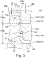
- a semiconductor device 100 includes a semiconductor body 102 having a first main surface 104.
- a trench structure 106 extends into the semiconductor body 102 from the first main surface 104.
- the trench structure 106 includes a trench electrode structure 108 and a trench dielectric structure 110.
- the trench dielectric structure 110 includes a gate dielectric 1101 in an upper part 110a of the trench dielectric structure 110 and a gap 1102 in a lower part 110b of the trench dielectric structure 110.
- the gate dielectric 1101 may include or consist of a thermally grown silicon oxide layer, a deposited silicon oxide layer, e.g. a silicon oxide based on TEOS (tetraethyl-orthosilicate), or both.
- the trench electrode structure 108 includes a gate electrode 1081 adjoining the gate dielectric 1101 in the upper part of the trench dielectric structure 110.
- the gate electrode 1081 of the trench electrode structure 108 is merged with a lower part of the trench electrode structure 108 that is configured as a field electrode and has a smaller width than the gate electrode 1081.
- a width wg of the gap 1102 tapers toward a transition point TP between the gap 1102 and the gate dielectric 1101.
- the width wg of the gap 1102 is constant or almost constant along a predominant vertical extent of the gap 1102.
- a p-doped body region 112 adjoins the gate dielectric 1101 at a sidewall 114 of the trench structure 106 in the upper part 110a of the trench dielectric structure 110.
- the gate dielectric 1101 extends deeper into the semiconductor body 102 along the sidewall 114 than the body region 112.
- an n + -doped source region 116 adjoins the gate dielectric 1101 at the sidewall 114 of the trench structure 106 in the upper part 110a.
- An n-doped drift region 118 adjoins the sidewall 114 in the lower part 110b of the trench dielectric structure 110. Vertical extension and dopant concentration in the drift region 118 are selected such that the semiconductor device 100 reaches its nominal blocking voltage capability.
- the drift region 118 may be formed in a layer grown by epitaxy.
- a mean net dopant concentration may be in the range from 1.0 x 10 15 cm -3 to 5.0 x 10 16 cm -3 .
- a vertical extension of the drift region 118 is related to the nominal blocking capability of the semiconductor device 100.
- the vertical extension of the drift region 118 may be in the range of about 1 ⁇ m to several 10 ⁇ m or in the range between 5 ⁇ m and 12 ⁇ m.
- further doped regions may be arranged, for example barrier zones and/or current spread regions of the conductivity type of the drift region 118 or counter-doped regions.
- each current spread region may directly adjoin or may be below the body region 112.
- a mean net dopant concentration in the current spread regions may be higher than in the drift region 118.
- the source region 116 and the body region 112 are electrically connected to a first load electrode L1, e.g. a front side load electrode or front side load pad.
- the front side electrode is one example of a first load electrode L1.
- the first load electrode L1 is, for example, the source terminal in case the semiconductor device 100 is an IGFET, or an emitter terminal in case the semiconductor device 100 is an IGBT.
- a variety of contact schemes may be used to electrically connect the source region 112 and the body region 112 to the first load electrode L1, e.g. by groove contacts or by parts of a mesa along a longitudinal direction of the mesa where the body region 112 extends to the first main surface 104 for being electrically connected. These and further contact variations are illustrated in the cross-sectional views of Figs. 1 to 3 in a simplified manner by contact nodes within the body region 112 and within the source region 116.
- the drift region 118 is electrically coupled to a second load electrode L2, e.g. a rear side electrode, which may directly adjoin a second main surface opposite to the first main surface 104 (not illustrated in Fig. 1 ).
- the rear side electrode is one example of second load electrode L2, which may be the drain terminal in case the semiconductor device 100 is an IGFET, or a collector terminal in case the semiconductor device 100 is an IGBT.
- the trench electrode 108 is electrically connected to a control electrode C, e.g. a front side control electrode or front side control pad.
- a control electrode C e.g. a front side control electrode or front side control pad.
- the front side control electrode is one example of a control electrode C.
- the trench electrode structure 108 includes the gate electrode 1081 adjoining the gate dielectric 1101 in the upper part 110a of the trench dielectric structure 110.
- the trench electrode structure 108 further includes a field electrode 1082 adjoining the gap 1102 in the lower part 110b of the trench dielectric structure 110.
- the trench dielectric structure 110 further includes an intermediate dielectric 1103 between the gate electrode 1081 and the field electrode 1082.
- a thickness t2 of the intermediate dielectric 1103 is at least two times larger than a thickness t1 of the gate dielectric 1101.
- the intermediate dielectric 1083 may include or consist of a thermally grown silicon oxide layer, a deposited silicon oxide layer, e.g. a silicon oxide based on TEOS (tetraethyl-orthosilicate), or both.
- a top part 126 of the gap 1102 is laterally limited by the semiconductor body 102 on one side and by the intermediate dielectric 1103 on the other side.
- the width wg of the gap 1102 continuously tapers from a bottom side 122 of the trench structure 106 towards the gate dielectric 1101.
- tapering of the gap 1102 is predominantly caused by a taper angle of the field electrode 1082.
- An alternative or additional option for adjusting tapering of the gap 1102 is a taper angle of the sidewall 114 of the trench structure 106.
- an interface 120 between the gap 1102 and the trench electrode structure 108 has a step 124 for adjusting tapering of the gap 1102.
- the measures for adjusting tapering of the gap 1102 described above may be combined, i.e. taper of the sidewall 114 adjoining the gap 1102, taper of interface between the gap 1102 and the field electrode 1082, step in the sidewall 114 adjoining the gap 1102 and step in the interface between the gap 1102 and the field electrode 1082 may be combined in any way.
- the semiconductor device 100 illustrated in Figs. 1 to 3 may be an IGBT (insulated gate bipolar transistor), or an IGFET (insulated gate field effect transistor), for example, a MOSFET (metal oxide semiconductor FET).
- IGBT insulated gate bipolar transistor
- IGFET insulated gate field effect transistor
- MOSFET metal oxide semiconductor FET
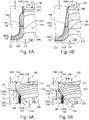
- FIG. 4A and 4B are based on the examples of semiconductor devices illustrated in Figs. 1 and 2 , respectively, and further illustrate electric equipotential lines EPL during a reverse blocking mode of the semiconductor device 100. Transition of the electric equipotential lines into the drift region 118 may be improved by tapering the gap 1102 of the trench dielectric structure 110.
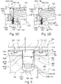
- FIG. 5A The schematic cross-sectional views of Figs. 5A to 5D are based on a semiconductor device including the intermediate dielectric 1103 (see e.g. Figs. 2 , 3 ) and exemplify various shapes of the top part 126 of the gap 1102 for transferring electric equipotential lines EPL from the gap 1102 into the drift region 118 and into the intermediate dielectric 1103.
- the top part 126 of the gap 1102 in the illustrated examples has a cross-sectional shape in the form of a rectangle (see Fig. 5A ), a semicircle (see Fig. 5B ), a quarter circle (see Fig. 5C ), and a triangle (see Fig. 5D ).
- the shape of the top part 126 of the gap 1102 may be designed depending on process technology and aims at diverging the equipotential lines EPL from the gap 1102 into intermediate dielectric 1103 and the drift region 118 similar to a diverging lens in optics.
- a thickness t2 of the intermediate dielectric 1103 may be at least two times larger than a thickness t1 of the gate dielectric 1101.
- a transition point TP is located between the gap 1102 and the intermediate dielectric 1103 at the sidewall 114.
- a first distance dt1 between the transition point TP and the gate electrode 1081 is larger than a second distance dt2 between the transition point TP and the field electrode 1082.
- the first distance dt1 may also be approximately equal to the second distance dt2, for example.
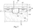
- FIG. 6 Another example of a semiconductor device 100 is illustrated in the schematic cross-sectional view of Fig. 6 .
- the semiconductor device 100 of Fig. 6 further includes a second field electrode 1083 and a second intermediate dielectric 1104 between the second field electrode 1083 and the field electrode 1082.
- a part of the first load electrode L1 is a groove contact electrically connected to the source region 116 and the body region 112.
- a highly p-doped body contact region 1122 may be arranged between the groove contact and the body region 112 for improving an ohmic contact characteristic, for example.
- An interlayer dielectric 128 is arranged between the first load electrode L1 and the first main surface 104. Apart from one (see Figs.
- field electrodes may be independently processed for achieving even more flexibility for adjusting shape and tapering the gap 1102, for example.
- the semiconductor device 100 includes a trench structure 106 extending into the semiconductor body 102 from the first main surface 104.
- the trench structure 106 includes a gate electrode 1081 and a gate dielectric 1101.
- the gate dielectric 1101 in the example of Fig. 7 is a gap arranged between the gate electrode 1081 and the semiconductor body 102.
- the gap may be filled with a gas having a pressure of less than 1atm, and a maximum width of the gap may range from 5nm to 50nm, for example.
- the transistor cells TC may be p-channel FET cells with n-doped body region 112, p-doped source region 116 and p-doped drift region 118.
- the field electrodes 1082, 1083 described with reference to the figures above may be electrically connected to the first load electrode L1, to another terminal of the semiconductor device 100, to an output of an internal or external driver circuit, or may float. In case of multiple field electrodes per trench structure, the multiple field electrodes may be coupled to identical or different potentials.
Landscapes
- Electrodes Of Semiconductors (AREA)
Priority Applications (3)
| Application Number | Priority Date | Filing Date | Title |
|---|---|---|---|
| EP21164244.2A EP4064364A1 (fr) | 2021-03-23 | 2021-03-23 | Dispositif à semi-conducteur comprenant une structure de tranchée |
| US17/695,207 US12349401B2 (en) | 2021-03-23 | 2022-03-15 | Semiconductor device including a trench structure having a trench dielectric structure with a gap |
| CN202210289294.9A CN115117156A (zh) | 2021-03-23 | 2022-03-23 | 包括沟槽结构的半导体器件 |
Applications Claiming Priority (1)
| Application Number | Priority Date | Filing Date | Title |
|---|---|---|---|
| EP21164244.2A EP4064364A1 (fr) | 2021-03-23 | 2021-03-23 | Dispositif à semi-conducteur comprenant une structure de tranchée |
Publications (1)
| Publication Number | Publication Date |
|---|---|
| EP4064364A1 true EP4064364A1 (fr) | 2022-09-28 |
Family
ID=75202964
Family Applications (1)
| Application Number | Title | Priority Date | Filing Date |
|---|---|---|---|
| EP21164244.2A Pending EP4064364A1 (fr) | 2021-03-23 | 2021-03-23 | Dispositif à semi-conducteur comprenant une structure de tranchée |
Country Status (3)
| Country | Link |
|---|---|
| US (1) | US12349401B2 (fr) |
| EP (1) | EP4064364A1 (fr) |
| CN (1) | CN115117156A (fr) |
Families Citing this family (4)
| Publication number | Priority date | Publication date | Assignee | Title |
|---|---|---|---|---|
| US20240290882A1 (en) * | 2023-02-23 | 2024-08-29 | Infineon Technologies Austria Ag | Semiconductor device having silicon plugs for trench and/or mesa segmentation |
| US20240363699A1 (en) * | 2023-04-27 | 2024-10-31 | Infineon Technologies Austria Ag | Semiconductor device having a trench structure with lower, upper, and intermediary sections and method of producing the semiconductor device |
| CN120164877A (zh) * | 2023-12-13 | 2025-06-17 | 达尔科技股份有限公司 | 垂直式功率半导体器件及其制造方法 |
| DE102024121365A1 (de) | 2024-07-26 | 2026-01-29 | Infineon Technologies Austria Ag | Halbleitervorrichtung und verfahren zum bilden eines leitfähigen elements und einer dielektrischen struktur in einem graben |
Citations (5)
| Publication number | Priority date | Publication date | Assignee | Title |
|---|---|---|---|---|
| US20090114986A1 (en) * | 2005-08-31 | 2009-05-07 | Infineon Technologies Austria Ag | Field plate trench transistor and method for producing it |
| US20090294843A1 (en) * | 2008-05-30 | 2009-12-03 | Freescale Semiconductor, Inc. | Enclosed void cavity for low dielectric constant insulator |
| US20100264486A1 (en) * | 2009-04-20 | 2010-10-21 | Texas Instruments Incorporated | Field plate trench mosfet transistor with graded dielectric liner thickness |
| US20170263767A1 (en) * | 2016-03-08 | 2017-09-14 | Kabushiki Kaisha Toshiba | Semiconductor device |
| US10304933B1 (en) * | 2018-04-24 | 2019-05-28 | Semiconductor Components Industries, Llc | Trench power MOSFET having a trench cavity |
Family Cites Families (12)
| Publication number | Priority date | Publication date | Assignee | Title |
|---|---|---|---|---|
| DE10014660C2 (de) | 2000-03-24 | 2002-08-29 | Infineon Technologies Ag | Halbleiteranordnung mit einer durch einen Hohlraum von einer Driftstrecke getrennten Trenchelektrode |
| US20060273385A1 (en) * | 2005-06-06 | 2006-12-07 | M-Mos Semiconductor Sdn. Bhd. | Trenched MOSFET device with contact trenches filled with tungsten plugs |
| DE102007063728B4 (de) * | 2006-03-07 | 2018-12-13 | Infineon Technologies Ag | Halbleiterbauelementanordnung mit einem Trench-Transistor |
| WO2012006261A2 (fr) * | 2010-07-06 | 2012-01-12 | Maxpower Semiconductor Inc. | Dispositifs à semi-conducteurs de puissance, structures et procédés associés |
| US8907408B2 (en) * | 2012-03-26 | 2014-12-09 | Infineon Technologies Austria Ag | Stress-reduced field-effect semiconductor device and method for forming therefor |
| US9245960B2 (en) * | 2013-02-08 | 2016-01-26 | Globalfoundries Inc. | Lateral extended drain metal oxide semiconductor field effect transistor (LEDMOSFET) with tapered airgap field plates |
| DE102016108949B4 (de) | 2016-05-13 | 2023-02-09 | Infineon Technologies Austria Ag | Halbleitervorrichtungen und Verfahren zum Herstellen einer Halbleitervorrichtung |
| DE102017101672B4 (de) | 2017-01-27 | 2021-02-25 | Infineon Technologies Austria Ag | Verfahren zum Herstellen einer Isolationsstruktur mit einer gasgefüllten Kavität und Halbleiterbauelement |
| JP6840611B2 (ja) * | 2017-04-21 | 2021-03-10 | 株式会社東芝 | 半導体装置及びその製造方法 |
| EP3621116B1 (fr) | 2018-09-06 | 2022-11-02 | Infineon Technologies Austria AG | Dispositif semi-conducteur et son procédé de fabrication |
| CN112397591B (zh) * | 2020-11-11 | 2022-06-17 | 武汉新芯集成电路制造有限公司 | 包含ldmos晶体管的半导体器件及制作方法 |
| JP7474214B2 (ja) * | 2021-03-17 | 2024-04-24 | 株式会社東芝 | 半導体装置 |
-
2021
- 2021-03-23 EP EP21164244.2A patent/EP4064364A1/fr active Pending
-
2022
- 2022-03-15 US US17/695,207 patent/US12349401B2/en active Active
- 2022-03-23 CN CN202210289294.9A patent/CN115117156A/zh active Pending
Patent Citations (5)
| Publication number | Priority date | Publication date | Assignee | Title |
|---|---|---|---|---|
| US20090114986A1 (en) * | 2005-08-31 | 2009-05-07 | Infineon Technologies Austria Ag | Field plate trench transistor and method for producing it |
| US20090294843A1 (en) * | 2008-05-30 | 2009-12-03 | Freescale Semiconductor, Inc. | Enclosed void cavity for low dielectric constant insulator |
| US20100264486A1 (en) * | 2009-04-20 | 2010-10-21 | Texas Instruments Incorporated | Field plate trench mosfet transistor with graded dielectric liner thickness |
| US20170263767A1 (en) * | 2016-03-08 | 2017-09-14 | Kabushiki Kaisha Toshiba | Semiconductor device |
| US10304933B1 (en) * | 2018-04-24 | 2019-05-28 | Semiconductor Components Industries, Llc | Trench power MOSFET having a trench cavity |
Also Published As
| Publication number | Publication date |
|---|---|
| US20220310838A1 (en) | 2022-09-29 |
| US12349401B2 (en) | 2025-07-01 |
| CN115117156A (zh) | 2022-09-27 |
Similar Documents
| Publication | Publication Date | Title |
|---|---|---|
| US10199456B2 (en) | Method of manufacturing a semiconductor device having a charge compensation region underneath a gate trench | |
| US12349401B2 (en) | Semiconductor device including a trench structure having a trench dielectric structure with a gap | |
| US9947741B2 (en) | Field-effect semiconductor device having pillar regions of different conductivity type arranged in an active area | |
| CN103383966B (zh) | 具有改善的鲁棒性的半导体器件 | |
| US11575032B2 (en) | Vertical power semiconductor device and manufacturing method | |
| CN103915485A (zh) | 电荷补偿半导体器件 | |
| US20250366146A1 (en) | Transistor device and method of manufacturing | |
| US20240413229A1 (en) | Semiconductor device having first trenches with a gate electrode and second trenches with a source electrode | |
| US20250151324A1 (en) | Vertical power semiconductor device including a sensor electrode | |
| EP4468361A1 (fr) | Transistor à effet de champ à jonction en tranchée comprenant une région mesa | |
| US12550387B2 (en) | Trench junction field effect transistor having a mesa region | |
| US12527075B2 (en) | Insulated gate bipolar transistor | |
| CN112909084B (zh) | 包括绝缘栅双极晶体管的半导体器件 | |
| EP4345911A1 (fr) | Transistor vertical à effet de champ à jonction comprenant une pluralité de régions mesa | |
| EP4704515A1 (fr) | Transistor à effet de champ à grille isolée comprenant une structure de tranchée | |
| US20250374593A1 (en) | Field effect transistor having a trench gate structure | |
| EP4583166A1 (fr) | Transistor bidirectionnel à effet de champ à jonction | |
| US20250056869A1 (en) | Wide band gap semiconductor device | |
| EP4465365A1 (fr) | Dispositif semi-conducteur de puissance vertical | |
| US20240371772A1 (en) | Vertical power semiconductor device having an interlayer dielectric structure | |
| US20240030323A1 (en) | Power Semiconductor Device and Method of Producing a Power Semiconductor Device | |
| CN116895701A (zh) | 半导体二极管以及制造方法 |
Legal Events
| Date | Code | Title | Description |
|---|---|---|---|
| PUAI | Public reference made under article 153(3) epc to a published international application that has entered the european phase |
Free format text: ORIGINAL CODE: 0009012 |
|
| STAA | Information on the status of an ep patent application or granted ep patent |
Free format text: STATUS: THE APPLICATION HAS BEEN PUBLISHED |
|
| AK | Designated contracting states |
Kind code of ref document: A1 Designated state(s): AL AT BE BG CH CY CZ DE DK EE ES FI FR GB GR HR HU IE IS IT LI LT LU LV MC MK MT NL NO PL PT RO RS SE SI SK SM TR |
|
| STAA | Information on the status of an ep patent application or granted ep patent |
Free format text: STATUS: REQUEST FOR EXAMINATION WAS MADE |
|
| 17P | Request for examination filed |
Effective date: 20230216 |
|
| RBV | Designated contracting states (corrected) |
Designated state(s): AL AT BE BG CH CY CZ DE DK EE ES FI FR GB GR HR HU IE IS IT LI LT LU LV MC MK MT NL NO PL PT RO RS SE SI SK SM TR |