EP4064542A1 - Circuit de conversion de tension et système d'alimentation électrique - Google Patents
Circuit de conversion de tension et système d'alimentation électrique Download PDFInfo
- Publication number
- EP4064542A1 EP4064542A1 EP20893678.1A EP20893678A EP4064542A1 EP 4064542 A1 EP4064542 A1 EP 4064542A1 EP 20893678 A EP20893678 A EP 20893678A EP 4064542 A1 EP4064542 A1 EP 4064542A1
- Authority
- EP
- European Patent Office
- Prior art keywords
- voltage
- voltage conversion
- winding
- low
- direct
- Prior art date
- Legal status (The legal status is an assumption and is not a legal conclusion. Google has not performed a legal analysis and makes no representation as to the accuracy of the status listed.)
- Withdrawn
Links
Images


Classifications
-
- H—ELECTRICITY
- H02—GENERATION; CONVERSION OR DISTRIBUTION OF ELECTRIC POWER
- H02M—APPARATUS FOR CONVERSION BETWEEN AC AND AC, BETWEEN AC AND DC, OR BETWEEN DC AND DC, AND FOR USE WITH MAINS OR SIMILAR POWER SUPPLY SYSTEMS; CONVERSION OF DC OR AC INPUT POWER INTO SURGE OUTPUT POWER; CONTROL OR REGULATION THEREOF
- H02M3/00—Conversion of DC power input into DC power output
- H02M3/22—Conversion of DC power input into DC power output with intermediate conversion into AC
- H02M3/24—Conversion of DC power input into DC power output with intermediate conversion into AC by static converters
- H02M3/28—Conversion of DC power input into DC power output with intermediate conversion into AC by static converters using discharge tubes with control electrode or semiconductor devices with control electrode to produce the intermediate AC
- H02M3/325—Conversion of DC power input into DC power output with intermediate conversion into AC by static converters using discharge tubes with control electrode or semiconductor devices with control electrode to produce the intermediate AC using devices of a triode or a transistor type requiring continuous application of a control signal
- H02M3/335—Conversion of DC power input into DC power output with intermediate conversion into AC by static converters using discharge tubes with control electrode or semiconductor devices with control electrode to produce the intermediate AC using devices of a triode or a transistor type requiring continuous application of a control signal using semiconductor devices only
- H02M3/3353—Conversion of DC power input into DC power output with intermediate conversion into AC by static converters using discharge tubes with control electrode or semiconductor devices with control electrode to produce the intermediate AC using devices of a triode or a transistor type requiring continuous application of a control signal using semiconductor devices only having at least two simultaneously operating switches on the input side, e.g. "double forward" or "double (switched) flyback" converter
-
- H—ELECTRICITY
- H02—GENERATION; CONVERSION OR DISTRIBUTION OF ELECTRIC POWER
- H02M—APPARATUS FOR CONVERSION BETWEEN AC AND AC, BETWEEN AC AND DC, OR BETWEEN DC AND DC, AND FOR USE WITH MAINS OR SIMILAR POWER SUPPLY SYSTEMS; CONVERSION OF DC OR AC INPUT POWER INTO SURGE OUTPUT POWER; CONTROL OR REGULATION THEREOF
- H02M3/00—Conversion of DC power input into DC power output
- H02M3/22—Conversion of DC power input into DC power output with intermediate conversion into AC
- H02M3/24—Conversion of DC power input into DC power output with intermediate conversion into AC by static converters
- H02M3/28—Conversion of DC power input into DC power output with intermediate conversion into AC by static converters using discharge tubes with control electrode or semiconductor devices with control electrode to produce the intermediate AC
- H02M3/325—Conversion of DC power input into DC power output with intermediate conversion into AC by static converters using discharge tubes with control electrode or semiconductor devices with control electrode to produce the intermediate AC using devices of a triode or a transistor type requiring continuous application of a control signal
- H02M3/335—Conversion of DC power input into DC power output with intermediate conversion into AC by static converters using discharge tubes with control electrode or semiconductor devices with control electrode to produce the intermediate AC using devices of a triode or a transistor type requiring continuous application of a control signal using semiconductor devices only
- H02M3/33569—Conversion of DC power input into DC power output with intermediate conversion into AC by static converters using discharge tubes with control electrode or semiconductor devices with control electrode to produce the intermediate AC using devices of a triode or a transistor type requiring continuous application of a control signal using semiconductor devices only having several active switching elements
- H02M3/33576—Conversion of DC power input into DC power output with intermediate conversion into AC by static converters using discharge tubes with control electrode or semiconductor devices with control electrode to produce the intermediate AC using devices of a triode or a transistor type requiring continuous application of a control signal using semiconductor devices only having several active switching elements having at least one active switching element at the secondary side of an isolation transformer
- H02M3/33584—Bidirectional converters
-
- H—ELECTRICITY
- H02—GENERATION; CONVERSION OR DISTRIBUTION OF ELECTRIC POWER
- H02J—ELECTRIC POWER NETWORKS; CIRCUIT ARRANGEMENTS OR SYSTEMS FOR SUPPLYING OR DISTRIBUTING ELECTRIC POWER; SYSTEMS FOR STORING ELECTRIC ENERGY
- H02J7/00—Circuit arrangements for charging or discharging batteries or for supplying loads from batteries
- H02J7/865—Battery or charger load switching, e.g. concurrent charging and load supply
-
- H—ELECTRICITY
- H02—GENERATION; CONVERSION OR DISTRIBUTION OF ELECTRIC POWER
- H02M—APPARATUS FOR CONVERSION BETWEEN AC AND AC, BETWEEN AC AND DC, OR BETWEEN DC AND DC, AND FOR USE WITH MAINS OR SIMILAR POWER SUPPLY SYSTEMS; CONVERSION OF DC OR AC INPUT POWER INTO SURGE OUTPUT POWER; CONTROL OR REGULATION THEREOF
- H02M1/00—Details of apparatus for conversion
- H02M1/36—Means for starting or stopping converters
-
- H—ELECTRICITY
- H02—GENERATION; CONVERSION OR DISTRIBUTION OF ELECTRIC POWER
- H02M—APPARATUS FOR CONVERSION BETWEEN AC AND AC, BETWEEN AC AND DC, OR BETWEEN DC AND DC, AND FOR USE WITH MAINS OR SIMILAR POWER SUPPLY SYSTEMS; CONVERSION OF DC OR AC INPUT POWER INTO SURGE OUTPUT POWER; CONTROL OR REGULATION THEREOF
- H02M3/00—Conversion of DC power input into DC power output
- H02M3/01—Resonant DC/DC converters
-
- H—ELECTRICITY
- H02—GENERATION; CONVERSION OR DISTRIBUTION OF ELECTRIC POWER
- H02M—APPARATUS FOR CONVERSION BETWEEN AC AND AC, BETWEEN AC AND DC, OR BETWEEN DC AND DC, AND FOR USE WITH MAINS OR SIMILAR POWER SUPPLY SYSTEMS; CONVERSION OF DC OR AC INPUT POWER INTO SURGE OUTPUT POWER; CONTROL OR REGULATION THEREOF
- H02M3/00—Conversion of DC power input into DC power output
- H02M3/22—Conversion of DC power input into DC power output with intermediate conversion into AC
- H02M3/24—Conversion of DC power input into DC power output with intermediate conversion into AC by static converters
- H02M3/28—Conversion of DC power input into DC power output with intermediate conversion into AC by static converters using discharge tubes with control electrode or semiconductor devices with control electrode to produce the intermediate AC
- H02M3/325—Conversion of DC power input into DC power output with intermediate conversion into AC by static converters using discharge tubes with control electrode or semiconductor devices with control electrode to produce the intermediate AC using devices of a triode or a transistor type requiring continuous application of a control signal
- H02M3/335—Conversion of DC power input into DC power output with intermediate conversion into AC by static converters using discharge tubes with control electrode or semiconductor devices with control electrode to produce the intermediate AC using devices of a triode or a transistor type requiring continuous application of a control signal using semiconductor devices only
- H02M3/33507—Conversion of DC power input into DC power output with intermediate conversion into AC by static converters using discharge tubes with control electrode or semiconductor devices with control electrode to produce the intermediate AC using devices of a triode or a transistor type requiring continuous application of a control signal using semiconductor devices only with automatic control of the output voltage or current, e.g. flyback converters
-
- H—ELECTRICITY
- H02—GENERATION; CONVERSION OR DISTRIBUTION OF ELECTRIC POWER
- H02M—APPARATUS FOR CONVERSION BETWEEN AC AND AC, BETWEEN AC AND DC, OR BETWEEN DC AND DC, AND FOR USE WITH MAINS OR SIMILAR POWER SUPPLY SYSTEMS; CONVERSION OF DC OR AC INPUT POWER INTO SURGE OUTPUT POWER; CONTROL OR REGULATION THEREOF
- H02M3/00—Conversion of DC power input into DC power output
- H02M3/22—Conversion of DC power input into DC power output with intermediate conversion into AC
- H02M3/24—Conversion of DC power input into DC power output with intermediate conversion into AC by static converters
- H02M3/28—Conversion of DC power input into DC power output with intermediate conversion into AC by static converters using discharge tubes with control electrode or semiconductor devices with control electrode to produce the intermediate AC
- H02M3/325—Conversion of DC power input into DC power output with intermediate conversion into AC by static converters using discharge tubes with control electrode or semiconductor devices with control electrode to produce the intermediate AC using devices of a triode or a transistor type requiring continuous application of a control signal
- H02M3/335—Conversion of DC power input into DC power output with intermediate conversion into AC by static converters using discharge tubes with control electrode or semiconductor devices with control electrode to produce the intermediate AC using devices of a triode or a transistor type requiring continuous application of a control signal using semiconductor devices only
- H02M3/33569—Conversion of DC power input into DC power output with intermediate conversion into AC by static converters using discharge tubes with control electrode or semiconductor devices with control electrode to produce the intermediate AC using devices of a triode or a transistor type requiring continuous application of a control signal using semiconductor devices only having several active switching elements
- H02M3/33573—Full-bridge at primary side of an isolation transformer
Definitions
- This application relates to the field of direct-current voltage conversion technologies, and in particular, to the field of bidirectional direct-current voltage conversion circuit and power system technologies.
- a precharge circuit is usually disposed between the high-voltage storage battery and the load capacitor.
- the precharge circuit needs to include at least a relay and a high-power line current resistor.
- Existence of the precharge circuit increases complexity of disposing electrical components in the power system, and increases a size.
- overall costs of the power system are relatively high due to a relatively large quantity of components in the precharge circuit.
- Embodiments of this application provide a voltage conversion circuit and a power system, to synchronously feed back, to a high-voltage conversion module, demagnetized energy generated when a low-voltage conversion module converts a low voltage into a high voltage, so that the voltage conversion circuit has relatively high voltage conversion efficiency and relatively low costs.
- an embodiment of this application provides a voltage conversion circuit, including a high-voltage conversion module, an isolation transformer, a low-voltage conversion module, and a feedback module.
- the high-voltage conversion module converts, along a first direction by using the isolation transformer and the low-voltage conversion module, a first direct-current voltage received from a first port into a second direct-current voltage.
- the first direct-current voltage is greater than the second direct-current voltage.
- the low-voltage conversion module receives the second direct-current voltage from a second port, and converts the second direct-current voltage into the first direct-current voltage along a second direction by using the isolation transformer and the high-voltage conversion module.
- the first direction is opposite to the second direction.
- the feedback module is configured to: induce, through electromagnetic induction, electric energy generated when the low-voltage conversion module converts the second direct-current voltage into the first direct-current voltage along the second direction, and transfer the induced electric energy to the high-voltage conversion module.
- the feedback module feeds back, to the high-voltage conversion module through electromagnetic induction, a part of electric energy generated in the low-voltage conversion module; and outputs, to a load capacitor connected to the first port, the electric energy together with the first direct-current voltage into which the second direct-current voltage is converted, thereby effectively improving precharge efficiency of the load capacitor, and effectively reducing a precharge time.
- the high-voltage conversion module is configured to convert the first direct-current voltage into a first alternating signal along the first direction.
- the low-voltage conversion module is configured to convert the second direct-current voltage into a second alternating signal along the second direction.
- the isolation transformer is electrically connected to the high-voltage conversion module and the low-voltage conversion module, and is configured to: at different times, convert the first alternating signal into a first converted alternating signal along the first direction and transmit the first converted alternating signal to the low-voltage conversion module, or convert the second alternating signal into a second converted alternating signal along the second direction and transmit the second converted alternating signal to the high-voltage conversion module.
- the low-voltage conversion module is further configured to convert the first converted alternating signal into the second direct-current voltage
- the high-voltage conversion module is further configured to convert the second converted alternating signal into the first direct-current voltage.
- the feedback module induces electric energy generated by the low-voltage conversion module when the low-voltage conversion module converts the second direct-current voltage into the second alternating signal.
- the low-voltage conversion module cooperates with the feedback module to feed back, by using the feedback module through electromagnetic induction, the demagnetized energy to the high-voltage conversion module, so that conversion efficiency of the low-voltage conversion module is effectively improved.
- the low-voltage conversion module includes a low-voltage filter circuit
- the low-voltage filter circuit includes a filter winding and a filter capacitor.
- the filter winding serves as a filter inductor and constitutes a filter circuit with the filter capacitor to filter the first converted alternating signal.
- the filter winding is in an exciting state for storing electric energy or a demagnetizing state for releasing electric energy at different times.
- the feedback module induces electric energy through electromagnetic induction when the filter winding is in the exciting state for storing electric energy, and feeds back the induced electric energy to the high-voltage conversion module when the filter winding is in the demagnetizing state for releasing electric energy.
- the filter winding performs filtering or excitation/demagnetization at different times to enable the voltage conversion circuit to perform bidirectional voltage conversion along the first direction and the second direction.
- the low-voltage conversion module further includes a low-voltage switch circuit, and the low-voltage switch circuit electrically connects the filter winding to the filter capacitor.
- the low-voltage switch circuit constitutes an excitation path for the filter winding in an excitation time period
- the low-voltage switch circuit constitutes a freewheeling path for the filter winding to release electric energy in a demagnetization time period.
- the excitation time period and the freewheeling time period are alternately set in terms of time to convert the second direct-current voltage into the second alternating signal.
- the feedback module obtains electric energy through electromagnetic induction in the excitation time period, and releases the induced electric energy and feeds back the induced electric energy to the high-voltage conversion module in the demagnetization time period.
- the low-voltage switch circuit is turned on or cut off under control of an external switch signal, so that the filter winding is flexibly in an exciting or demagnetizing state.
- the feedback module includes a demagnetizing winding, a switching control unit, and a unidirectional transfer unit, and the unidirectional transfer unit, the demagnetizing winding, and the switching control unit are electrically connected to the first port in sequence.
- the demagnetizing winding and the filter winding constitute an electromagnetic coupler.
- the switching control unit is configured to: when the high-voltage conversion module performs voltage conversion to the low-voltage conversion module along the first direction, control the demagnetizing winding not to be in a conducting path, so that the feedback module does not feed back energy; and when the low-voltage conversion module performs voltage conversion to the high-voltage conversion module along the second direction, control the demagnetizing winding to be in a conducting path, so that the feedback module feeds back energy to the high-voltage conversion module.
- the unidirectional transfer unit is configured to control a current flow direction of the conducting path in which the demagnetizing winding is located to be the second direction.
- the demagnetizing winding transfers, by using the unidirectional transfer unit, the demagnetized energy obtained from the filter winding to the high-voltage conversion module and the first port, thereby improving efficiency of converting the second direct-current voltage into the first direct-current voltage, and effectively preventing loss of the demagnetized energy.
- the switching control unit controls the conducting path in which the demagnetizing winding is located to be in an electrically off state, no electromagnetic induction occurs between the filter winding and the demagnetizing winding, and the filter winding serves as a filter inductor.
- the switching control unit controls the conducting path in which the demagnetizing winding is located to be in an electrically on state, electromagnetic induction occurs between the filter winding and the demagnetizing winding, and the filter winding transmits, to the high-voltage conversion module, obtained electric energy rectified by the unidirectional transfer unit.
- the switching control unit Under control of the switching control unit, whether the feedback module cooperates with the low-voltage conversion module to perform electromagnetic induction can be accurately controlled. Further, when the low-voltage conversion module is configured to output the second direct-current voltage, the demagnetizing winding and the filter winding do not perform electromagnetic induction, thereby accurately outputting the second direct-current voltage to the second port while reducing power consumption of electronic elements in the feedback module.
- the isolation transformer includes a first winding and a second winding.
- the first winding is electrically connected to the high-voltage conversion module, and the second winding is electrically connected to the low-voltage switch circuit.
- the low-voltage switch circuit controls the second winding to be electromagnetically coupled to the first winding, to rectify the first converted alternating signal.
- the converting the second direct-current voltage into the second alternating signal includes:
- the low-voltage switch circuit controls the filter winding to be excited for storing electric energy and output a first direct-current voltage of a first phase in a first excitation sub-time period of the excitation time period.
- the low-voltage switch circuit controls the filter winding to be demagnetized for releasing electric energy in the demagnetization time period.
- the low-voltage switch circuit controls the filter winding to be excited for storing electric energy and output a first direct-current voltage of a second phase in a second excitation sub-time period of the excitation time period, where the first phase is opposite to the second phase.
- the low-voltage switch circuit controls the filter winding to be demagnetized for releasing electric energy in the demagnetization time period.
- the first excitation sub-time period of the excitation time period, the demagnetization time period, and the second excitation sub-time period of the excitation time period are continuous in terms of time and do not overlap.
- first winding and the second winding perform electromagnetic induction and energy transfer can be accurately controlled by turning on and cutting off the low-voltage switch circuit, so that the low-voltage conversion module accurately converts the second direct-current voltage into a direct-current voltage by using the isolation transformer and outputs the direct-current voltage to the high-voltage conversion module.
- the second winding includes two series-connected sub-windings
- the low-voltage switch circuit includes two switch elements
- the two switch elements are respectively electrically connected to the two sub-windings, and are configured to control the two sub-windings to be electromagnetically coupled to the first winding.
- the two switch elements in the low-voltage switch circuit respectively control the two sub-windings to be electromagnetically coupled to the first winding at different times, and separately control electric energy stored in the filter winding to generate the second alternating signal.
- the two switch elements control the two sub-windings not to be electromagnetically coupled to the first winding, to control the filter winding to be demagnetized for releasing stored electric energy.
- the two switch elements in the low-voltage switch circuit respectively control the two sub-windings to be electromagnetically coupled to the first winding at different times, to output the first converted alternating signal, and the two switch elements rectify the first converted alternating signal.
- An electromagnetically coupled state of the two sub-windings can be controlled by using the two switch elements, so that cooperative control on the second winding and the low-voltage conversion module is more convenient and accurate.
- the high-voltage conversion module includes a high-voltage filter circuit and a high-voltage switch circuit, and the high-voltage filter circuit and the high-voltage switch circuit are connected in series between the first port and the isolation transformer.
- the high-voltage filter circuit is configured to filter the first direct-current voltage received or output from the first port.
- the high-voltage switch circuit is configured to: convert the first alternating signal into the first alternating signal, or rectify a signal obtained by converting the second direct-current voltage input by the isolation transformer and the low-voltage conversion module.
- the high-voltage filter circuit cooperates with the high-voltage switch circuit so that the high-voltage conversion module accurately performs conversion between the first direct-current voltage and the second direct-current voltage.
- an embodiment of this application provides a power system, including the foregoing voltage conversion circuit, a high-voltage storage battery, and a low-voltage storage battery.
- the high-voltage storage battery is electrically connected to the first port, and the low-voltage storage battery is electrically connected to the second port.
- the high-voltage storage battery is configured to receive or output the first direct-current voltage, and the low-voltage storage battery is configured to receive or output the second direct-current voltage.
- the power system can effectively improve precharge efficiency of a load capacitor and effectively reduce a precharge time.
- the voltage conversion circuit precharges a load capacitor in a load after receiving the second direct-current voltage from the low-voltage storage battery and converting the second direct-current voltage into the first direct-current voltage along the second direction.
- the high-voltage storage battery can drive the load capacitor and other functional circuits in the load by providing the first direct-current voltage. Because precharge efficiency of the load capacitor is improved, a startup speed of the other functional circuits in the load is also increased.
- FIG. 1 is a functional block diagram of a power system 1 according to an embodiment of this application.
- the power system 1 may be applied to a power-driven apparatus such as an automobile or an electric automobile, and the power system 1 includes a voltage conversion circuit 10, a high-voltage storage battery 11, a low-voltage storage battery 12, and a load 13.
- the high-voltage storage battery 11 is electrically connected to the load 13, and is electrically connected to the voltage conversion circuit 10 through a first port P1.
- the high-voltage storage battery 11 is configured to provide a first direct-current voltage VI for driving a load capacitor C0 and a functional circuit 130 in the load 13.
- the functional circuit 130 may be a circuit that needs to use electric power as a driving force and that performs different functions in a power-driven apparatus such as a motor controller circuit, an air pump controller circuit, or an oil pump controller circuit.
- the high-voltage storage battery 11 outputs the first direct-current voltage VI to the voltage conversion circuit 10 through the first port P1, and the voltage conversion circuit 10 performs buck conversion and then provides a voltage obtained through buck conversion to the low-voltage storage battery 12 for energy storage and charging; or the high-voltage storage battery 11 receives, through the first port PI, the first direct-current voltage VI obtained by the voltage conversion circuit 10 by performing boost conversion.
- the low-voltage storage battery 12 is electrically connected to the voltage conversion circuit 10 through a second port P2.
- the low-voltage storage battery 12 is configured to output a second direct-current voltage V2.
- the voltage conversion circuit 10 converts the second direct-current voltage V2 into the first direct-current voltage V1 to precharge the load capacitor C0.
- the precharge is to provide a relatively small charging current to charge the load capacitor C0 before the high-voltage storage battery 11 provides the first direct-current voltage V1 to the load capacitor C0 and the functional circuit, to avoid damage to the high-voltage storage battery 11 caused by a relatively large charging current generated due to an excessively large voltage difference between the first direct-current voltage V1 and the load capacitor C0 in a short time.
- the high-voltage storage battery 11 totally does not need to provide other precharge circuits to precharge the load capacitor C0, circuit complexity of the power system 1 is effectively reduced, and a size and costs are also reduced.
- the high-voltage storage battery 11 can drive the load capacitor C0 and other functional circuits in the load 13 by providing the first direct-current voltage. Because precharge efficiency of the load capacitor C0 is improved, a startup speed of the other functional circuits in the load is also increased.
- the voltage conversion circuit 10 can further convert the first direct-current voltage V1 output by the high-voltage storage battery 11 into the second direct-current voltage V2, and provide the second direct-current voltage V2 to the low-voltage storage battery 12 for charging the low-voltage storage battery 12. To be specific, in different time periods, the voltage conversion circuit 10 can convert the first direct-current voltage V1 output by the high-voltage storage battery 11 into the second direct-current voltage V2, or convert the second direct-current voltage V2 output by the low-voltage storage battery 12 into the first direct-current voltage VI, to implement bidirectional conversion between the first direct-current voltage V1 and the second direct-current voltage V2.
- the first direct-current voltage V1 is greater than the second direct-current voltage V2.
- the first direct-current voltage V1 is mainly used to drive a high-power power circuit, and the second direct-current voltage V2 is mainly used to drive a low-power control circuit.
- the first direct-current voltage V1 may be greater than 200 to 350 volts (V)
- the second direct-current voltage V2 may be 9 to 16 V
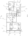
- FIG. 2 is a functional block diagram of the voltage conversion circuit 10 shown in FIG. 1 .
- the voltage conversion circuit 10 configured to perform bidirectional direct-current voltage conversion includes a high-voltage conversion module 101, an isolation transformer 102, a low-voltage conversion module 103, and a feedback module 104.
- the high-voltage conversion module 101 and the low-voltage conversion module 103 are separately electrically connected to the isolation transformer 102.
- the first direct-current voltage V1 is converted into the second direct-current voltage V2 along a first direction F1 through cooperation between the high-voltage conversion module 101, the isolation transformer 102, and the low-voltage conversion module 103.
- the second direct-current voltage V2 is converted into the first direct-current voltage V1 along a second direction F2 opposite to the first direction F1 through cooperation between the low-voltage conversion module 103, the isolation transformer 102, and the high-voltage conversion module 101, thereby implementing bidirectional conversion between the first direct-current voltage V1 and the second direct-current voltage V2.
- the feedback module 104 is configured to: feed back, to the high-voltage conversion module 101 through electromagnetic induction, a part of electric energy generated in the low-voltage conversion module 103; and output, to the load capacitor C0, the electric energy together with the first direct-current voltage V1 into which the second direct-current voltage V2 is converted, thereby effectively improving precharge efficiency of the load capacitor C0, and effectively reducing a precharge time.
- the low-voltage conversion module 103 precharges the load capacitor C0 by using the first direct-current voltage V1 obtained through conversion by the isolation transformer 102 and the high-voltage conversion module.
- the feedback module 104 further feeds back the induced electric energy together with the first direct-current voltage V1 to the high-voltage conversion module 101 to precharge the load capacitor C0, so that a precharge time can be reduced.
- the precharge time may be controlled within milliseconds.
- the feedback module 104 is not in an operating state.
- the high-voltage conversion module 101 when low-voltage conversion is implemented along the first direction F1, the high-voltage conversion module 101 is electrically connected to the high-voltage energy storage battery 11 through the first port P1, and is configured to: receive the first direct-current voltage V1 from the high-voltage energy storage battery 11, convert the first direct-current voltage V1 into a first alternating signal along the first direction F1, and transmit the first alternating signal to the isolation transformer 102.
- the isolation transformer 102 continues to convert the first alternating signal into a first converted alternating signal along the first direction F1, and transmits the first converted alternating signal to the low-voltage conversion module 103.
- the low-voltage conversion module 103 converts the received first converted alternating signal into the second direct-current voltage V2.
- the first port P1 includes a high-voltage bus terminal VH+ and a low-voltage bus VH-.
- the high-voltage bus terminal VH+ and the low-voltage bus VH- cooperate to receive or output the first direct-current voltage V1.
- the low-voltage bus VH- may be a first ground terminal GND1.
- the low-voltage conversion module 103 is electrically connected to the low-voltage energy storage battery 12 through the second port P2, and is configured to: receive the second direct-current voltage V2 from the low-voltage storage battery 12, convert the second direct-current voltage V2 into a second alternating signal, and transmit the second alternating signal to the isolation transformer 102.
- the isolation transformer 102 converts the second alternating signal into a second converted alternating signal along the second direction F2, and transmits the second converted alternating signal to the high-voltage conversion module 101.
- the high-voltage conversion module 101 converts the received second converted alternating signal into the first direct-current voltage V1.
- the second port P2 includes a high-voltage reference terminal VL+ and a low-voltage reference terminal VL-.
- the low-voltage bus V- may be a second ground terminal GND2.
- the first ground terminal GND1 is different from the second ground terminal GND2.
- the first ground terminal GND1 is a high-voltage analog ground
- the second ground terminal GND2 is a low-voltage reference ground, for example, a digital ground.
- the high-voltage conversion module 101 includes a high-voltage filter circuit HF and a high-voltage switch circuit HS.
- the high-voltage filter circuit HF is electrically connected to the first port P1
- the high-voltage switch circuit HS electrically connects the high-voltage filter circuit to a first winding T11 of the isolation transformer 102.
- the high-voltage filter circuit HF is configured to filter the first direct-current voltage VI
- the high-voltage switch circuit HS is configured to convert a filtered first direct-current voltage V1 into the first alternating signal.
- the high-voltage switch circuit HS When the second converted alternating signal is input to the high-voltage conversion module 101 along the second direction F2, the high-voltage switch circuit HS directly outputs the second converted alternating signal to the high-voltage filter circuit HF for filtering, and then transmits a filtered second converted alternating signal to the first port P1.
- the isolation transformer 102 includes the first winding T11 and a second winding T12.
- the first winding T11 and the second winding T12 are isolated from each other and constitute an electromagnetic coupler. To be specific, only magnetic coupling but no electrical connection relationship exists between the first winding T11 and the second winding T12.
- an alternating magnetic flux is induced between the first winding T11 and the second winding T12 to generate an induced voltage on the second winding T12, to convert the voltage signal received by the first winding T11 into another voltage signal output by the second winding T12.
- Conversion between different voltages on the first winding T11 and the second winding T12 can be implemented by setting a quantity of coils in the first winding T11 and the second winding T12.
- the second winding T12 further includes two series-connected sub-windings T12a and T12b.
- the two sub-windings T12a and T12b are not in an electromagnetically coupled state at the same time.
- the sub-windings T12a and T12b are electromagnetically coupled to the first winding T11 at different times.
- the low-voltage conversion module 103 includes a low-voltage switch circuit LS and a low-voltage filter circuit LF.
- the low-voltage switch circuit LS is electrically connected to the second winding T12.
- the low-voltage filter circuit LF is electrically connected between the low-voltage switch circuit LS and the second port P2.
- the low-voltage filter circuit LF includes a filter winding T21 and a filter capacitor Cf.
- the filter winding T21 and the low-voltage filter capacitor Cf are electrically connected to the low-voltage switch circuit LS and the second port P2.
- the low-voltage switch circuit LS controls the sub-windings T12a and T12b to be in an electromagnetically coupled state at different times, to rectify the first converted alternating signal and transmit a rectified first converted alternating signal to the filter winding T21 and the low-voltage filter capacitor Cf in the low-voltage filter circuit LF.
- the filter winding T21 and the low-voltage filter capacitor Cf filter the rectified first converted alternating signal to obtain the second direct-current voltage V1.
- the filter winding T21 serves only as a filter inductor, and cooperates with the filter capacitor Cf to filter the second converted alternating signal
- the filter winding T21 in the low-voltage filter circuit HF is in an exciting state for storing energy or a demagnetizing state for releasing energy, in cooperation with the low-voltage switch circuit HS.
- the filter winding T21 is in the exciting state for storing energy, the first direct-current voltage signal V2 is converted into the second alternating signal, and the second alternating signal is provided to the second winding T21.
- the feedback module 104 and the filter winding T21 are in an electromagnetically coupled state, that is, the feedback module 104 and the filter winding T21 constitute an electromagnetic coupler.
- the feedback module 104 provides a demagnetization loop for the feedback module 104 so that the filter winding T21 releases stored electric energy, and the feedback module 104 converts the electric energy released by the filter winding T21 into a feedback voltage Vf, and feeds back and transmits the feedback voltage Vf to the first port P1. Both the feedback voltage Vf and the second direct-current voltage V2 are provided to the first port P1, thereby effectively improving precharge efficiency of the load capacitor C0.
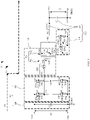
- FIG. 3 is a schematic diagram of a specific circuit structure of a voltage conversion circuit 10 shown in FIG. 2 according to an embodiment of this application.
- the load capacitor C0 is reused as the high-voltage filter circuit HF, and the load capacitor C0 is electrically connected to the high-voltage bus terminal V+ and the low-voltage bus terminal V- of the first port.
- the high-voltage switch circuit HS includes a full-bridge switch circuit that includes four switch elements.
- the four switch elements are a first switch S1, a second switch S1, a third switch S3, and a fourth switch S4, the first switch S1 and the second switch S2 constitute a first bridge arm (branch) AMI, and the third switch S3 and the fourth switch S4 constitute a fourth bridge arm (branch) AM2.
- the first bridge arm AMI and the first bridge arm AM2 are connected in parallel.
- the first bridge arm AMI includes a first transmit terminal NA
- the first bridge arm AMI includes a second transmit terminal NA'.
- the first transmit terminal NA and the second transmit terminal NA' cooperate to output the first alternating signal or receive the second converted alternating signal.
- the first switch S1 includes a first control terminal CS1, a first conducting terminal ES1, and a second conducting terminal ES2.
- the second switch S2 includes a second control terminal CS2, a third conducting terminal ES3, and a fourth conducting terminal ES4.
- the first control terminal CS1 is configured to receive a first control signal PS1
- the second control terminal CS2 is configured to receive a second control signal PS2.
- the first control signal PS1 and the second control signal PS2 are pulse signals with a same duty cycle and a same frequency but opposite phases.
- the first control signal PS1 and the second control signal PS2 are pulse width modulation (Pulse Width Modulation, PWM) signals, and a duty cycle of the pulse width modulation signals may be set within a range of 0 to 100% according to an actual requirement. For example, 50% may be selected.
- the first conducting terminal ES1 is electrically connected to the high-voltage bus terminal VH+, and the second conducting terminal ES2 is electrically connected to the first transmission NA.
- the third conducting terminal ES3 is electrically connected to the first inverter output terminal NA, and the fourth conducting terminal ES4 is electrically connected to the low-voltage bus terminal VL-.
- the second conducting terminal ES2 and the third conducting terminal ES3 are directly electrically connected.
- the first switch S1 and the second switch S2 are metal-oxide-semiconductor (metal-oxide-semiconductor, MOS) field effect transistors.
- MOS metal-oxide-semiconductor
- the first control terminal CS1 is a gate G (not marked) of the MOS transistor
- the first conducting terminal ES1 is a drain D (not marked) of the MOS transistor
- the second conducting terminal ES2 is a source S (not marked) of the MOS transistor.
- the second control terminal CS2 is a gate G (not marked) of the MOS transistor
- the third conducting terminal ES3 is a drain D (not marked) of the MOS transistor
- the fourth conducting terminal ES4 is a source S (not marked) of the MOS transistor.
- the third switch S3 includes a third control terminal CS3, a fifth conducting terminal ES5, and a sixth conducting terminal ES6.
- the fourth switch S4 includes a fourth control terminal CS4, a seventh conducting terminal ES7, and an eighth conducting terminal ES8.
- the third control terminal CS3 is configured to receive a third control signal PS3, and the fourth control terminal CS4 is configured to receive a fourth control signal PS4.
- the third control signal PS3 and the fourth control signal PS4 are PWM signals with a same frequency but opposite phases.
- the fifth conducting terminal ES5 is electrically connected to the high-voltage bus terminal VH+, and the sixth conducting terminal ES6 is electrically connected to the second transmit terminal NA'.
- the seventh conducting terminal ES7 is electrically connected to the second transmit terminal NA', and the eighth conducting terminal ES8 is electrically connected to the low-voltage bus V-.
- the third control terminal CS3 is a gate G (not marked) of the MOS transistor
- the fifth conducting terminal ES5 is a drain D (not marked) of the MOS transistor
- the sixth conducting terminal ES6 is a source S (not marked) of the MOS transistor.
- the fourth control terminal CS2 is a gate G (not marked) of the MOS transistor
- the seventh conducting terminal ES7 is a drain D (not marked) of the MOS transistor
- the eighth conducting terminal ES8 is a source S (not marked) of the MOS transistor.
- the first switch S1 to the fourth switch S4 of the four switch elements are all N-channel MOS transistors.
- the isolation transformer module 102 includes a first transformer T1 that is constituted by the first winding T11 and the second winding T12, and a resonant circuit 1021.
- the resonant circuit is electrically connected between the high-voltage switch circuit HS and the first winding T11.
- the first transformer T1 further includes a first connection terminal T1a, a second connection terminal T1b, a third connection terminal T1c, a fourth connection terminal T1d, and a fifth connection terminal T1e.
- the first winding T11 is electrically connected between the first connection terminal T1a and the second connection terminal T1b.
- the sub-winding T12a is electrically connected between the third connection terminal T1c and the fourth connection terminal T1d.
- the sub-winding T12b is electrically connected between the third connection terminal T1c and the fifth connection terminal T1e.
- the third connection terminal T1c also serves as a central tap of the second winding T12.
- an iron core (not marked) is further disposed between the first winding T11 and the second winding T12, and the first winding T11 is electromagnetically coupled to the second winding T12, to implement voltage conversion between the two windings.
- the resonant circuit 1021 includes a first resonant capacitor Cr and a resonant inductor Lr that are connected in series to the first transmit terminal NA and the first connection terminal T2a, and the resonant circuit 1021 is configured to filter out an interference signal in the first alternating signal.
- the resonant circuit 1021 may be alternatively omitted.
- the low-voltage switch circuit LS includes a switch circuit that includes two switch elements.
- the two switch elements are a fifth switch S5 and a sixth switch S6.
- the fifth switch S5 includes a fifth control terminal CS5, an eleventh conducting terminal ES11, and a twelfth conducting terminal ES12.
- the sixth switch S6 includes a sixth control terminal CS6, a thirteenth conducting terminal ES13, and a fourteenth conducting terminal ES 14.
- the fifth control terminal CS5 is configured to receive a fifth control signal PS5
- the sixth control terminal CS6 is configured to receive a sixth control signal PS6.
- the eleventh conducting terminal ES11 is electrically connected to the fifth connection terminal T1e, and the twelfth conducting terminal ES2 is electrically connected to the second ground terminal GND2.
- the thirteenth conducting terminal ES13 is electrically connected to the fourth connection terminal T1d, and the fourteenth conducting terminal ES14 is electrically connected to the second ground terminal GND2.
- the fifth control terminal CS5 is a gate G (not marked) of the MOS transistor
- the eleventh conducting terminal ES11 is a drain D (not marked) of the MOS transistor
- the twelfth conducting terminal ES12 is a source S (not marked) of the MOS transistor.
- the sixth control terminal CS6 is a gate G (not marked) of the MOS transistor
- the thirteenth conducting terminal ES13 is a drain D (not marked) of the MOS transistor
- the fourteenth conducting terminal ES 14 is a source S (not marked) of the MOS transistor.
- the filter winding T21 is electrically connected between the third connection terminal T1c and the high-voltage reference terminal VL+ of the second port P2.
- the filter capacitor Cf is electrically connected between the high-voltage reference terminal VL+ and the low-voltage reference terminal VL- of the second port P2.
- the feedback module 104 includes a demagnetizing winding T22, a unidirectional transfer unit 1041, and a switching control unit 1042.
- the unidirectional transfer unit 1041, the demagnetizing winding T22, and the switching control unit 1042 are electrically connected between the high-voltage bus terminal V+ and the low-voltage bus terminal V- of the first interface P1 in sequence.
- the low-voltage terminal V- is the first ground terminal GND1.
- a location of the demagnetizing winding T22 is set so that the demagnetizing winding T22 and the filter winding T21 constitute an electromagnetic coupler, that is, the demagnetizing winding T22 and the filter winding T21 constitute a flyback transformer T2.
- Locations of the unidirectional transfer unit 1041 and the switching control unit 1042 are adjacent to those of the high-voltage filter circuit HF and the high-voltage switch circuit HS in the high-voltage conversion module 101.
- the switching control unit 1042 is configured to selectively control whether the demagnetizing winding T22 is in a conducting path. To be specific, the switching control unit 1042 controls the demagnetizing winding T22 not to be in a conducting path when the voltage conversion circuit 10 performs low-voltage conversion along the first direction F1, so that the filter winding T21 performs only a filtering function; and controls the demagnetizing winding T22 to be in a conducting loop when the voltage conversion circuit 10 performs high-voltage conversion along the second direction F2.
- the unidirectional transfer unit 1041 is configured to control a current flow direction of the conducting path in which the demagnetizing winding T22 is located to be the second direction F2.
- the unidirectional transfer unit 1041 includes a feedback diode D1.
- An end of the demagnetizing winding T21 that is away from a switch element K1 is electrically connected to an anode of the feedback diode D1.
- a cathode of the feedback diode D1 is electrically connected to the high-voltage bus terminal VH+ of the first port P1.
- the switching control unit 1041 may use the switch element K1 to control whether to form a conducting path.
- the switch element K1 is electrically connected between the first ground terminal GND1 and an end of the demagnetizing winding T21 that is away from the feedback diode D1.
- the switch element K1 may be a relay, a mechanical switch, or a transistor.
- the switch element K1 is in an on state or a cut-off state depending on whether the voltage conversion circuit 10 performs low-voltage conversion along the first direction F1 or high-voltage conversion along the second direction F2. Specifically, the switch element K1 is in the cut-off state when the voltage conversion circuit 10 performs low-voltage conversion along the first direction F1, and is in the on state when the voltage conversion circuit 10 performs high-voltage conversion along the second direction F2.
- the demagnetizing winding T21 When the switch element K1 is in the on state, the demagnetizing winding T21 is in the conducting loop. When the switch element K1 is in the cut-off state, no conducting path is formed in a circuit in which the demagnetizing winding T21 is located, that is, the demagnetizing winding T21 cannot form an induced current or an induced electromotive force, and therefore does not feed back electric energy obtained through electromagnetic induction to the high-voltage conversion module 101.
- FIG. 4 is a schematic diagram of circuit conduction when the voltage conversion circuit 10 performs low-voltage conversion along the first direction F1.
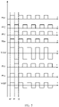
- FIG. 5 is a schematic diagram of voltage waveforms of nodes when the voltage conversion circuit 10 performs low-voltage conversion along the first direction F1.
- the voltage conversion circuit 100 performs low-voltage conversion along the first direction F1.
- the feedback unit 104 is not in an operating state.
- the voltage conversion circuit 100 performs low-voltage conversion along the first direction F1 and high-voltage conversion along the second direction F2 at different times. To be specific, voltage conversion in only one direction is performed at one time, and voltage conversion in two directions may be performed separately in different time periods.
- the high-voltage conversion module 101 receives the first direct-current voltage V1 from the first port P1, the high-voltage filter circuit HF filters the first direct-current voltage V1, and the high-voltage switch circuit HS converts the filtered first direct-current voltage V1 into the first alternating signal.
- the four switch elements in the high-voltage switch circuit HS are in a corresponding on or cut-off state under control of the corresponding first control signal PS 1 to the corresponding fourth control signal PS4 respectively.
- the first control signal PS1 and the fourth control signal PS4 respectively control the first switch S1 and the fourth switch S4 to be in an on state
- the second control signal PS2 and the third control signal PS3 respectively control the second switch S2 and the third switch S3 to be in a cut-off state.
- the first transmit terminal NA and the second transmit terminal NA' cooperate to output a positive first direct-current voltage V1.
- the first transmit terminal NA and the second transmit terminal NA' cooperate to output a negative first direct-current voltage V1.
- the first transmit terminal NA and the second transmit terminal NA' cooperate to output the positive first direct-current voltage V1 and the negative first direct-current voltage V1 that change alternately.
- the positive first direct-current voltage V1 and the negative first direct-current voltage V1 that change alternately constitute the first alternating signal.
- a symbol VAA' in FIG. 5 indicates a voltage waveform diagram of the first alternating signal output by the first transmit terminal NA and the second transmit terminal NA'.
- the first winding T11 of the isolation transformer 102 When the first winding T11 of the isolation transformer 102 receives the first alternating signal, the first winding T11 is electromagnetically coupled to the second winding T12, so that an induced voltage and an induced current are generated on both the sub-windings T12a and T12b of the second winding T12.
- the fifth control signal PS5 controls the fifth switch S5 to be in an on state
- the sixth control signal PS6 controls the sixth switch S6 to be in a cut-off state, that is, the sub-winding T21b is in a conducting loop.
- the sub-winding T21b generates an induced current and an induced voltage between the third connection terminal T1c and the fifth connection terminal T1e.
- the induced voltage between the third connection terminal T1c and the fifth connection terminal T1e is a positive first induced voltage, and is output from a node NB and a node NB'.
- the induced current is filtered by the filter winding T21 and the filter capacitor C2.
- the node NB is the third connection Tc1
- the node NB' is the second ground terminal GND2.
- the fifth control signal PS5 controls the fifth switch S5 to be in a cut-off state
- the sixth control signal PS6 controls the sixth switch S6 to be in an on state, that is, the sub-winding T21a is in a conducting loop.
- the sub-winding T21a generates an induced current and an induced voltage between the third connection terminal T1c and the fourth connection terminal T1d.
- the induced voltage between the third connection terminal T1c and the fourth connection terminal T1d is a negative first induced voltage, and is output from the nodes NB and NB'.
- the induced current is filtered by the filter winding T21 and the filter capacitor C2.
- the nodes NB and NB' cooperate to output the positive first induced voltage and the negative first induced voltage that change alternately, to constitute the second converted alternating signal.
- a symbol VBB' in FIG. 5 indicates a voltage waveform diagram of the second converted alternating signal output by the node NB and the node NB'.
- an induced current is filtered by the filter winding T21 and the filter capacitor C2, to obtain the second direct-current voltage V2, and the second direct-current voltage V2 is output to the second port P2.
- FIG. 6 is a schematic diagram of circuit conduction when a voltage conversion circuit 10 performs high-voltage conversion along a second direction F2.
- FIG. 7 is a schematic diagram of voltage waveforms of nodes when a voltage conversion circuit 10 performs high-voltage conversion along a second direction F2.
- the voltage conversion circuit 100 performs high-voltage conversion along the second direction F2.
- the feedback unit 104 is in an operating state.
- the low-voltage conversion module 103 receives the second direct-current voltage V2 from the second port P2, the filter capacitor filters the second direct-current voltage V2, and the low-voltage switch circuit LS is controlled so that the filter winding T21 is in an exciting state or a demagnetizing state at different times.
- the feedback unit 104 feeds back electric energy released by the filter winding T21 during demagnetization to the high-voltage conversion module 101.
- the low-voltage switch circuit LS generates the second alternating signal at the node NB and the node NB'.
- the second alternating signal is converted into the second converted alternating signal by the first transformer T1.
- the second converted alternating signal is transmitted from the first transmit terminal NA and the second transmit terminal NA' to the high-voltage switch circuit HS for rectification and to the high-voltage filter circuit HF for filtering, to obtain the first direct-current voltage V1 at the first port P1.
- the two switch elements in the low-voltage switch circuit LS are in a corresponding on or cut-off state under control of the corresponding fifth control signal PS5 and the corresponding sixth control signal PS6 respectively.
- the fifth control signal PS5 controls the fifth switch S5 to be in a cut-off state
- the sixth control signal PS6 controls the sixth switch S6 to be in an on state.
- the second direct-current voltage V2 excites the filter winding T21 for energy storage by using the sub-winding T21b in which the fifth switch S5 is located. Therefore, a current flowing through the filter winding T21 gradually increases, and a positive second direct-current voltage V2 is generated at the third connection terminal T12c and the fourth connection terminal T12d.
- the fifth control signal PS5 controls the fifth switch S5 to be in a cut-off state
- the sixth control signal PS6 controls the sixth switch S6 to be in a cut-off state.
- the filter winding T21 is demagnetized by using the demagnetizing winding T22 and releases electric energy.
- the filter winding T21 is not in a conducting loop. Therefore, in this case, no current flows through the filter winding T21. In other words, a current on the filter winding T21 is zero.
- a current on the demagnetizing winding T22 gradually decreases.
- an induced current on the demagnetizing winding T22 is rectified by the feedback diode D1 and filtered by the high-voltage filter circuit HF and then loaded to the first port P1.
- the fifth control signal PS5 controls the fifth switch S5 to be in an on state
- the sixth control signal PS6 controls the sixth switch S6 to be in a cut-off state.
- the second direct-current voltage V2 excites the filter winding T21 for energy storage by using the sub-winding T21a in which the sixth switch S5 is located. Therefore, a current flowing through the filter winding T21 gradually increases, and a positive second direct-current voltage V2 is generated at the third connection terminal T12c and the fifth connection terminal T12e.
- VBB' shown in FIG. 7 indicates a voltage waveform of the second alternating signal
- the demagnetizing winding T22 provides a freewheeling path for the filter winding T21, to ensure that the low-voltage conversion module 103 can accurately convert the second direct-current voltage V2 into the first alternating signal.
- the first winding T11 is electromagnetically coupled to the second winding T12, to generate an induced voltage and an induced current on the first winding T11, and further constitute the second converted alternating signal at the first transmit terminal NA and the second transmit terminal NA'.
- VAA' shown in FIG. 7 indicates a voltage waveform of the second converted alternating signal.
- the fifth control signal PS5 controls the fifth switch S5 to be in a cut-off state
- the sixth control signal PS6 controls the sixth switch S6 to be in a cut-off state.
- the filter winding T21 is demagnetized by using the demagnetizing winding T22 and releases electric energy.
- the filter winding T21 is not in a conducting loop. Therefore, in this case, no current flows through the filter winding T21. In other words, a current on the filter winding T21 is zero.
- a current on the demagnetizing winding T22 gradually decreases.
- an induced current on the demagnetizing winding T22 is rectified by the feedback diode D1 and filtered by the high-voltage filter circuit HF and then loaded to the first port P1.
- the first excitation sub-time period of t0 to t1 the demagnetization time period of t1 to t2, the second excitation sub-time period of t2 to t3, and the demagnetization time period of t3 to t4 are continuous in terms of time and do not overlap.
- the time period of t1 to t4 is merely a period of converting the second direct-current voltage V2 into the second alternating signal.
- a process of converting the second direct-current voltage V2 into the second alternating signal includes a plurality of consecutive periods, and the voltage conversion circuit 10 repeats an operating process of t1 to t4 in other periods. Details are not described herein again.
- the first control signal PS1 to the fourth control signal PS4 may be in a suspended state.
- the first switch S1 to the fourth switch S4 do not need to perform control, but a full-bridge rectifier circuit is constituted by body diodes in the first switch S1 to the fourth switch S4, to rectify the second converted alternating signal output by the first winding T11 from the first transmit terminal NA and the second transmit terminal NA'. Then the induced current is rectified by the high-voltage filter circuit HF to obtain the first direct-current voltage VI, and the first direct-current voltage V1 is loaded from the first port P1 to the load capacitor C0.
- FIG. 8 is a schematic diagram of a specific circuit structure of a voltage conversion circuit 20 according to another embodiment of this application.
- the voltage conversion circuit 20 is basically the same as the voltage conversion circuit 10 in FIG. 3 , except that a switching unit is a transistor S7.
- a source of the transistor S7 is electrically connected to a demagnetizing winding T22.
- the source and a drain of the transistor S7 are electrically connected to a first ground terminal GND.
- the source and a gate of the transistor S7 receive an external control signal.
- the transistor S7 is an N-channel MOS transistor.
- the gate of the transistor S7 receives a low-level control signal, and the transistor is controlled to be in a cut-off state, so that a circuit in which the demagnetizing winding T22 is located does not constitute a complete conducting loop, that is, there is no conducting path between a high-voltage bus terminal V+ and a low-voltage bus V- of the circuit in which the demagnetizing winding is located.
- the gate of the transistor S7 receives a high-level control signal, and the transistor S7 is controlled to be in an on state, so that the circuit in which the demagnetizing winding T22 is located does not constitute a complete conducting loop, that is, a conducting path is formed between the high-voltage bus terminal V+ and the low-voltage bus V- of the circuit in which the demagnetizing winding T22 is located.
- a current induced by the demagnetizing winding T22 from a filter winding T21 can be transmitted in the conducting loop.
Landscapes
- Engineering & Computer Science (AREA)
- Power Engineering (AREA)
- Dc-Dc Converters (AREA)
Applications Claiming Priority (2)
| Application Number | Priority Date | Filing Date | Title |
|---|---|---|---|
| CN201911219536.1A CN110932558B (zh) | 2019-11-29 | 2019-11-29 | 电压转换电路、电源系统 |
| PCT/CN2020/131964 WO2021104407A1 (fr) | 2019-11-29 | 2020-11-26 | Circuit de conversion de tension et système d'alimentation électrique |
Publications (2)
| Publication Number | Publication Date |
|---|---|
| EP4064542A1 true EP4064542A1 (fr) | 2022-09-28 |
| EP4064542A4 EP4064542A4 (fr) | 2022-12-28 |
Family
ID=69848559
Family Applications (1)
| Application Number | Title | Priority Date | Filing Date |
|---|---|---|---|
| EP20893678.1A Withdrawn EP4064542A4 (fr) | 2019-11-29 | 2020-11-26 | Circuit de conversion de tension et système d'alimentation électrique |
Country Status (3)
| Country | Link |
|---|---|
| EP (1) | EP4064542A4 (fr) |
| CN (1) | CN110932558B (fr) |
| WO (1) | WO2021104407A1 (fr) |
Cited By (1)
| Publication number | Priority date | Publication date | Assignee | Title |
|---|---|---|---|---|
| CN115776240A (zh) * | 2023-01-30 | 2023-03-10 | 广东优力普物联科技有限公司 | 一种大功率反激式升压电路 |
Families Citing this family (6)
| Publication number | Priority date | Publication date | Assignee | Title |
|---|---|---|---|---|
| CN110932558B (zh) * | 2019-11-29 | 2021-07-09 | 华为技术有限公司 | 电压转换电路、电源系统 |
| CN111509986A (zh) * | 2020-05-19 | 2020-08-07 | 深圳英飞源技术有限公司 | 双向移相全桥变换器的辅助缓启动和放电电路 |
| CN113302828B (zh) * | 2020-10-16 | 2023-11-17 | 深圳欣锐科技股份有限公司 | 电压转换电路与电子装置 |
| CN113300440B (zh) * | 2021-07-28 | 2021-10-15 | 苏州贝克微电子有限公司 | 一种电池供电装置及其供电方法 |
| CN116780668A (zh) * | 2022-01-10 | 2023-09-19 | 何小平 | 高压设备的一体化集成及高频传能供电装置与集成方法 |
| CN117811364B (zh) * | 2024-03-01 | 2024-06-11 | 深圳麦格米特电气股份有限公司 | 一种电压保持电路及方法、电源电路、电子设备 |
Family Cites Families (10)
| Publication number | Priority date | Publication date | Assignee | Title |
|---|---|---|---|---|
| JP4430531B2 (ja) * | 2004-12-28 | 2010-03-10 | 株式会社日立製作所 | 双方向絶縁型dc−dcコンバータ |
| JP4719567B2 (ja) * | 2005-12-21 | 2011-07-06 | 日立オートモティブシステムズ株式会社 | 双方向dc−dcコンバータおよびその制御方法 |
| US7768807B2 (en) * | 2007-05-14 | 2010-08-03 | Gm Global Technology Operations, Inc. | Bidirectional no load control with overshoot protection |
| JP4378400B2 (ja) * | 2007-08-28 | 2009-12-02 | 日立コンピュータ機器株式会社 | 双方向dc−dcコンバータ及び双方向dc−dcコンバータの制御方法 |
| DE102010024679A1 (de) * | 2010-06-24 | 2011-12-29 | Kaco New Energy Gmbh | Gleichstromsteller |
| JP5585408B2 (ja) * | 2010-11-16 | 2014-09-10 | Tdk株式会社 | スイッチング電源装置 |
| US9859803B2 (en) * | 2013-04-23 | 2018-01-02 | Analog Devices Global | Transformer-based isolated bi-directional DC-DC power converter, and method and controller for using same |
| CN104852586B (zh) * | 2015-05-27 | 2017-09-22 | 深圳科士达科技股份有限公司 | 一种双向dcdc转换器 |
| JP6924103B2 (ja) * | 2017-08-30 | 2021-08-25 | 株式会社Soken | 電力変換装置 |
| CN110932558B (zh) * | 2019-11-29 | 2021-07-09 | 华为技术有限公司 | 电压转换电路、电源系统 |
-
2019
- 2019-11-29 CN CN201911219536.1A patent/CN110932558B/zh active Active
-
2020
- 2020-11-26 WO PCT/CN2020/131964 patent/WO2021104407A1/fr not_active Ceased
- 2020-11-26 EP EP20893678.1A patent/EP4064542A4/fr not_active Withdrawn
Cited By (1)
| Publication number | Priority date | Publication date | Assignee | Title |
|---|---|---|---|---|
| CN115776240A (zh) * | 2023-01-30 | 2023-03-10 | 广东优力普物联科技有限公司 | 一种大功率反激式升压电路 |
Also Published As
| Publication number | Publication date |
|---|---|
| CN110932558A (zh) | 2020-03-27 |
| CN110932558B (zh) | 2021-07-09 |
| WO2021104407A1 (fr) | 2021-06-03 |
| EP4064542A4 (fr) | 2022-12-28 |
Similar Documents
| Publication | Publication Date | Title |
|---|---|---|
| EP4064542A1 (fr) | Circuit de conversion de tension et système d'alimentation électrique | |
| CN111355398B (zh) | 一种集成dc/dc转换器的双向车载充电机电路 | |
| JP4643695B2 (ja) | 双方向dc−dcコンバータ及びその制御方法 | |
| KR100689349B1 (ko) | D.c.-d.c. 컨버터 및 이 컨버터에서의 일차측 및 이차측간 절연 유지 방법 | |
| WO2019062086A1 (fr) | Chargeur à trois ports avec fonction d'inversion | |
| US20190027950A1 (en) | Bidirectional dc/dc converter and method for charging the intermediate circuit capacitor of a dc/dc converter from the low-voltage battery | |
| WO2011084742A2 (fr) | Conversion de signal bidirectionnelle | |
| CN102142776A (zh) | 开关电源装置 | |
| CN104159779A (zh) | 具有电机的车辆和用于运行该电机的方法 | |
| CN115868105A (zh) | 软开关脉冲宽度调制dc-dc功率转换器 | |
| CN104981971A (zh) | 正反激拓扑的开关模式电源 | |
| JP2015159711A (ja) | スイッチング電源装置、電力変換装置 | |
| KR102730545B1 (ko) | 차량용 전력 변환 시스템 및 그 제어 방법 | |
| EP2685620A1 (fr) | Convertisseur cc/cc bidirectionnel et système source d'énergie | |
| KR20180074300A (ko) | 48v 마일드하이브리드용 배터리 일체형 양방향 dc-dc 컨버터 | |
| JP2015177634A (ja) | 電流共振型dcdcコンバータ | |
| CN218102962U (zh) | Dc-dc转换器、用于电力供应和控制的系统及交通工具 | |
| WO2019177685A1 (fr) | Convertisseur dévolteur en cascade à inducteurs couplés à réponse transitoire rapide | |
| US20230097153A1 (en) | Switched-inductor power converter, communication system, and method | |
| JP5412515B2 (ja) | 電源装置 | |
| JP5135418B2 (ja) | 双方向dc−dcコンバータ | |
| JP5587382B2 (ja) | 双方向dc−dcコンバータ | |
| TW200919921A (en) | Synchronous self-driven power converter | |
| US6903944B2 (en) | Active clamp DC/DC converter with resonant transition system | |
| KR101695963B1 (ko) | 배터리 충방전 기능을 갖는 양방향 컨버터 회로 |
Legal Events
| Date | Code | Title | Description |
|---|---|---|---|
| STAA | Information on the status of an ep patent application or granted ep patent |
Free format text: STATUS: THE INTERNATIONAL PUBLICATION HAS BEEN MADE |
|
| PUAI | Public reference made under article 153(3) epc to a published international application that has entered the european phase |
Free format text: ORIGINAL CODE: 0009012 |
|
| STAA | Information on the status of an ep patent application or granted ep patent |
Free format text: STATUS: REQUEST FOR EXAMINATION WAS MADE |
|
| 17P | Request for examination filed |
Effective date: 20220621 |
|
| AK | Designated contracting states |
Kind code of ref document: A1 Designated state(s): AL AT BE BG CH CY CZ DE DK EE ES FI FR GB GR HR HU IE IS IT LI LT LU LV MC MK MT NL NO PL PT RO RS SE SI SK SM TR |
|
| A4 | Supplementary search report drawn up and despatched |
Effective date: 20221129 |
|
| RIC1 | Information provided on ipc code assigned before grant |
Ipc: H02M 1/00 20060101ALI20221123BHEP Ipc: H02M 3/00 20060101ALI20221123BHEP Ipc: H02M 1/36 20070101ALI20221123BHEP Ipc: H02M 3/335 20060101AFI20221123BHEP |
|
| DAV | Request for validation of the european patent (deleted) | ||
| DAX | Request for extension of the european patent (deleted) | ||
| STAA | Information on the status of an ep patent application or granted ep patent |
Free format text: STATUS: THE APPLICATION IS DEEMED TO BE WITHDRAWN |
|
| 18D | Application deemed to be withdrawn |
Effective date: 20230627 |