EP4064563B1 - Commutateur électronique - Google Patents
Commutateur électronique Download PDFInfo
- Publication number
- EP4064563B1 EP4064563B1 EP21164491.9A EP21164491A EP4064563B1 EP 4064563 B1 EP4064563 B1 EP 4064563B1 EP 21164491 A EP21164491 A EP 21164491A EP 4064563 B1 EP4064563 B1 EP 4064563B1
- Authority
- EP
- European Patent Office
- Prior art keywords
- electronic switch
- voltage
- suppressor diodes
- switching element
- current
- Prior art date
- Legal status (The legal status is an assumption and is not a legal conclusion. Google has not performed a legal analysis and makes no representation as to the accuracy of the status listed.)
- Active
Links
Images


Classifications
-
- H—ELECTRICITY
- H03—ELECTRONIC CIRCUITRY
- H03K—PULSE TECHNIQUE
- H03K17/00—Electronic switching or gating, i.e. not by contact-making and –breaking
- H03K17/08—Modifications for protecting switching circuit against overcurrent or overvoltage
- H03K17/081—Modifications for protecting switching circuit against overcurrent or overvoltage without feedback from the output circuit to the control circuit
- H03K17/0814—Modifications for protecting switching circuit against overcurrent or overvoltage without feedback from the output circuit to the control circuit by measures taken in the output circuit
- H03K17/08148—Modifications for protecting switching circuit against overcurrent or overvoltage without feedback from the output circuit to the control circuit by measures taken in the output circuit in composite switches
-
- H—ELECTRICITY
- H03—ELECTRONIC CIRCUITRY
- H03K—PULSE TECHNIQUE
- H03K17/00—Electronic switching or gating, i.e. not by contact-making and –breaking
- H03K17/16—Modifications for eliminating interference voltages or currents
- H03K17/168—Modifications for eliminating interference voltages or currents in composite switches
-
- H—ELECTRICITY
- H03—ELECTRONIC CIRCUITRY
- H03K—PULSE TECHNIQUE
- H03K2217/00—Indexing scheme related to electronic switching or gating, i.e. not by contact-making or -breaking covered by H03K17/00
- H03K2217/0063—High side switches, i.e. the higher potential [DC] or life wire [AC] being directly connected to the switch and not via the load
Definitions
- the invention relates to an electronic switch having a first and a second terminal, between which an electrically conductive connection can be established or interrupted, and having at least one bidirectional turn-off semiconductor switching element connected between the first and second terminals.
- semiconductor-based circuit breakers hereinafter referred to as electronic switches, could replace conventional miniature circuit breakers in both AC and DC networks. These switches interrupt the current path using semiconductor switches such as IGBTs.
- the electronic switch has at least one, but usually two, semiconductor switches connected in anti-serial or anti-parallel in the current path.
- Such electronic switches offer advantages in terms of the speed with which fault currents can be interrupted. This is advantageous, for example, in DC networks in future industrial plants, which are intended to reduce losses, ensure direct energy exchange between converters, storage systems, and motors, and achieve increased robustness.
- the short cable lengths result in very small series inductances in the supply lines, which in turn cause fault currents to exhibit a very steep rise.
- the necessary rapid interruption is achieved better by semiconductor switches than by mechanical switches, as semiconductor switches can interrupt the fault within a few hundred nanoseconds after detection.
- a capacitor can be installed in parallel with the semiconductor switches, which slows the voltage rise after shutdown to such an extent that the dissipation of the inductively stored energy is unproblematic.
- the electronic switch can also have a varistor, which is arranged either in series with the capacitor or between the poles of the power grid.
- Such solutions are known, for example, from WO 2019/011642 A1 and the WO 2020/099103 A1
- a disadvantage of the known solutions is that the capacitors used are large and heavy components, which contribute significantly to the overall size of the electronic switch.
- the electronic switch according to the invention has a first and a second terminal, between which an electrically conductive connection can be established or interrupted.
- the electronic switch with these terminals is serially integrated into a pole of an electrical network and can thus interrupt or establish the electrical connection in this pole.
- the electronic switch further comprises a bidirectional turn-off semiconductor switching element which is arranged between the first and second terminals, thus connecting the first and second terminals.
- a bidirectional turn-off semiconductor switching element which is arranged between the first and second terminals, thus connecting the first and second terminals.
- the electronic switch includes a voltage limiting circuit connected in parallel with the semiconductor switching element.
- the voltage limiting circuit includes multiple bidirectional suppressor diodes. In the case of multiple suppressor diodes, these are arranged in a series circuit. It is understood that the bidirectional suppressor diodes can be integrated components or individual unidirectional components connected in reverse series.
- suppressor diodes advantageously enable the limitation of a build-up of voltage across the semiconductor switch. Since this limitation occurs via a non-destructive breakdown of the suppressor diodes and causes a corresponding current flow, such a voltage limitation results in power loss in the suppressor diode. It has been found that suppressor diodes are available that can achieve a peak power of several tens of kW over a turn-off period of approximately 200 ⁇ s, which makes their use in modern DC networks possible even at operating voltages of, for example, 800 V and with inductively stored energies in the range of 1 to 50 J.
- suppressor diodes eliminates the need for a capacitor, which is otherwise often used for voltage limitation. Since suppressor diodes are significantly smaller and lighter than a capacitor dimensioned for the same network, this results in significant weight and space savings, even when using multiple suppressor diodes.
- the varistors used in known solutions also can be eliminated.
- Another advantage is that the suppressor diodes have an exceptionally high reaction speed, allowing them to achieve voltage limitation even with low line inductances and a correspondingly rapid current rise.
- the electronic switch comprises a capacitor arranged in parallel with one or more of the suppressor diodes. Measurements have shown that, despite the theoretically extremely fast response of the suppressor diodes to an overvoltage in a real circuit, the voltage initially significantly exceeds the summed breakdown voltage of the suppressor diodes and only drops to the range of the summed breakdown voltage after a time period in the range of 1 ⁇ s has elapsed.
- the term summed breakdown voltage is used, even if only one suppressor diode is present, in which case the summed breakdown voltage is precisely the breakdown voltage of the one suppressor diode.
- this initial overvoltage may be unproblematic or may make further measures advisable.
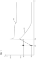
- Figure 1 shows a measured curve of the current 101 across an exemplary electronic switch as well as the curve of the voltage 102 across the electronic switch.
- the electronic switch has three suppressor diodes connected in series, but not the capacitor.
- the electronic switch is switched on at time 103, with a short circuit occurring directly on the load side of the switch.
- the current then rises and is switched off by the switch immediately after the fault is detected, resulting in a peak current of 470 A due to the inductance used.
- the voltage 102 shows a clear peak with a height of just over 1600 V.
- the capacitor is advantageously arranged in parallel with at least one of the suppressor diodes. This mitigates the initial voltage spike, as the affected suppressor diode(s) is initially bypassed until the capacitor is charged. As a result, only a reduced total breakdown voltage is present initially, and the initial voltage spike, which exceeds the breakdown voltages, is also correspondingly reduced.
- the suppressor diode(s) connected in parallel to the capacitor contribute with their breakdown voltage to the total counter voltage that is built up across the electronic switch.
- the capacitor used in the electronic switch does not have to dampen the voltage buildup across the electronic switch for the entire turn-off period, but only for a short initial period of less than 10 ⁇ s, its capacitance can be significantly smaller than in conventional solutions. Therefore, its size and weight are significantly smaller.
- the capacitor can be arranged in parallel to exactly one of the suppressor diodes.
- suppressor diodes are present, so that the capacitor is arranged in parallel with fewer than all of the suppressor diodes. It is advantageous if, in addition to the bridged suppressor diode(s), further suppressor diodes are arranged in series, since then, even at the moment of shutdown, a countervoltage is already built up against the inductively driven current flow, thus preventing the short-circuit current from building up further. This prevents a further buildup of inductively stored energy, which then has to be dissipated.
- the sum of the breakdown voltages of all suppressor diodes is less than the dielectric strength of the semiconductor switching element. This limits the voltage across the semiconductor switching element to a value that prevents damage to the semiconductor switching element.
- the sum of the breakdown voltages of all suppressor diodes is greater than 60%, in particular greater than 80%, and in a special embodiment, greater than 90% of the dielectric strength of the semiconductor switch.
- a summed breakdown voltage that is as high as possible allows the inductively driven current to dissipate more quickly after the electronic switch is turned off.
- the capacitor can advantageously have a capacitance of less than 10 ⁇ F, in particular less than 5 ⁇ F. In special embodiments, the capacitor can have a capacitance of less than 2 ⁇ F. It is thus significantly smaller than a typical capacitor used in known voltage limiting solutions, which has a capacitance of, for example, 50 ⁇ F.
- the semiconductor switching element comprises two anti-serial or anti-parallel connected semiconductor switches.
- Such circuits comprising two semiconductor switches, for example, two IGBTs, are available as integrated Modules, but they can also be present as individual and separate components.
- anti-serially connected switches these preferably comprise the known freewheeling diodes arranged in series.
- the semiconductor switches preferably have a dielectric strength of at least 600 V, in particular at least 1200 V.
- the electronic switch can have a pre-charging circuit.
- This comprises a series circuit with a switching device, for example another bidirectional semiconductor switching element, and a current-limiting resistor.
- the pre-charging circuit is connected in parallel to the semiconductor switching element, i.e., is also arranged between the first and second terminals.
- the pre-charging circuit can be used to charge capacitances present on the load side with a limited current flow before the electronic switch is switched on, i.e., to reduce the voltage difference between the two terminals before the actual switching on. This avoids the almost unlimited current flow that would otherwise occur when the electronic switch is switched on, provided there is a significant load-side capacitance.
- the electronic switch can advantageously be used in an electrical network, in particular a DC network.
- One such electronic switch or a plurality of electronic switches can be used in the network.
- the electronic switch is preferably connected with its first and second terminals to one pole of the network, so that the current path of the load current leads through the semiconductor switching element. It is advantageous if the summed breakdown voltage of the suppressor diodes is greater than the operating voltage of the electrical network, so that upon shutdown, a sufficient countervoltage is generated to completely dissipate the current.
- the electrical network preferably has an operating voltage of at least 400 V, in particular at least 800 V.
- the electronic switch can comprise a control device that controls the semiconductor switching element.
- the control device can be configured to measure the current flowing through the semiconductor switching element. The current measured by the control device thus corresponds to the current flowing in the network, i.e., the load current.
- the control device can further be configured to cause the semiconductor switching element to shut down if the current exceeds a threshold value.
- the threshold value is selected to be characteristic of a fault current. In this case, the electronic switch is therefore operated as a circuit breaker.
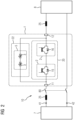
- the Figure 2 shows a DC voltage system 10 with a load 8, which is fed from a DC network 7.
- the DC voltage of the DC network 7 is applied between the first potential 41 and the second potential 42.
- An electronic switch 1 is arranged between the DC network 7 and the load 8.
- the electronic switch 1 also contains a contactor or isolator 80, which can be used to galvanically isolate the load 8 from the DC network 7.
- the contactor or isolator 80 is not absolutely necessary for the function of the electronic switch 1.
- the inductances present in the supply lines are represented by element 25. These can be parasitic inductances of lines or inductive components such as chokes, coils, or transformers.
- the electronic switch 1 has a series circuit of two turn-off semiconductor switches 2 between its first terminal 11 and its second terminal 12. These are arranged anti-serially to one another. This means that the switching element of the two turn-off semiconductor switches 2 can each carry a current with a different direction and thus switch. To increase the blocking capacity, i.e., the voltage to be switched, the number of turn-off semiconductor switches 2 in the series circuit 5 can be further increased.
- a diode 15, 16 is arranged antiparallel to the respective switching element of the turn-off semiconductor switch 2.
- a current can flow through the diode 15, 16 in the opposite direction to the current flowing through the corresponding switching element of the turn-off semiconductor switch 2.
- the antiserial arrangement of the two turn-off semiconductor switches 2 results in the current flowing between the first terminal 11 and the second terminal 12 through a diode of one turn-off semiconductor switch 2 and through a switching element of the other turn-off semiconductor switch 2.
- the series circuit of the turn-off semiconductor switches 2 is connected to the first potential 41 of the DC network 7.
- the electronic switch 1 also has two suppressor diodes 3, which form a series circuit 5.
- the Series circuit 5 is connected in parallel to the two semiconductor switches 2, i.e., just like these, between the first and second terminals 11, 12.
- the present DC voltage system 10 is a network with an operating voltage of 400 V.
- semiconductor switches 2 are to be used with a dielectric strength of 650 V.
- the specific number of suppressor diodes 3 results from a consideration of the existing parameters of the DC voltage system 10. If these are known, the number and type of selected suppressor diodes 3 can be adapted accordingly, as is the case in this example. If the parameters, for example the inductances connected to the electronic switch 1, are unknown, a configuration of the electronic switch 1 can be selected that functions in any case within the framework of minimum and maximum parameters, for example a minimum and maximum line inductance. In the first exemplary embodiment, it is assumed that a very high line inductance or possibly also a load inductance of 200 ⁇ H is connected to the electronic switch on the load side. This ensures that the current rise in the event of a fault is relatively slow. The time required to detect a fault plays only a minor role in this case, and the fault can be switched off even with a relatively low current. The voltage peak at the beginning of the shutdown process, as seen from Figure 1 - with other parameters - is therefore small.
- two suppressor diodes 3 of the type 30KPA216CA with a breakdown voltage of approximately 265 V can be selected. Others with a slightly higher breakdown voltage can also be selected, as long as the dielectric strength of the semiconductor switches 2 is not exceeded.
- six suppressor diodes 3 with a breakdown voltage of 95 V can also be used. can be selected. The number can be determined by considering, for example, the energy that the suppressor diodes 3 must absorb during shutdown. If the current during shutdown in this example is 200 A, then the peak power of the suppressor diodes 3 is 200 A * 265 V, or just over 50 kW.
- This peak power can be absorbed by the suppressor diodes 3 as long as the width of the current peak, which corresponds roughly to half the duration of the shutdown, is not greater than approximately 300 ⁇ s. If more than two suppressor diodes 3 are used, the power converted in each of the suppressor diodes 3 decreases in line with the lower voltage, and more time is available for the duration of the shutdown - at least with regard to the suppressor diodes 3.
- Figure 3 shows an electronic switch 1 according to a second example.
- the operating voltage of a second, not shown, DC voltage system is 800 V.
- those of the type 30KPA280CA are used here, whose breakdown voltage is 334 V.
- three suppressor diodes 3 connected in series are necessary, since only with three suppressor diodes 3 is the summed breakdown voltage higher than the operating voltage of 800 V.
- the semiconductor switches 2 used in the second example are intended to have a dielectric strength of 1200 V. To avoid repetition, reference is made to the description of Figure 2 and to the reference symbols introduced there.
- a real electronic switch 1, which is constructed according to the invention, in particular according to the embodiment of Figures 3 typically also includes a pre-charging circuit 30 as shown in Figure 3
- This pre-charging circuit 30 serves to charge the capacitances present on the load side before switching on the semiconductor switches 2 in order to avoid an extremely high inrush current.
- the capacitor 6 is connected in such a way that it bridges all existing suppressor diodes 3, then the pre-charging circuit is also advantageously used to discharge the capacitor 6 before switching on the semiconductor switches 2.
- the capacitor is as in Figure 3 shown connected in such a way that one or more suppressor diodes 3 remain in series with it, then at least for the capacitor 6 no discharge is necessary during a switch-on process.
- the second embodiment includes a capacitor 6 connected in parallel with a first of the three suppressor diodes 3.
- the capacitance of capacitor 6 in this embodiment is 1 ⁇ F, more than an order of magnitude less than typical capacitors in known suppression networks such as those mentioned in the introduction.
- the capacitor 6 ensures that at the first moment of commutation of the load current from the turn-off semiconductor switches 2 to the suppressor diodes 3, one of the suppressor diodes 3 is bypassed by the capacitor 6. At the moment of switch-off, the capacitor 6 is uncharged because, in the switched-on state, almost no voltage is dropped across the electronic switch 1.
- the breakdown voltage of the series circuit of suppressor diodes 3 is reduced by the breakdown voltage of such a suppressor diode 3, in this case by approximately 344 V to 688 V.
- the initially occurring overvoltage is thus also reduced to a value of approximately 1100 V, whereby semiconductor switches 2 with a dielectric strength of 1200 V can be used.
- the electronic switch 1 is designed for an operating current of 44 A and switches off at a five-fold overcurrent, i.e., at 220 A.
- the resulting power loss in one of the suppressor diodes 3 is therefore 220 A * 344 V, or approximately 75 kW.
- a peak power loss is possible for a current peak width of approximately 180 ⁇ s.
- Tests with an inductance of 230 ⁇ H, which is significantly oversized for typical line inductances, have shown that the resulting current peaks have a width in the range of a few ⁇ s, thus still providing considerable leeway. remains.
- the described operating mode therefore poses no problem for the suppressor diodes 3 used, even if, for example, the maximum clamping voltage is used to consider the peak power. Since a low line inductance was assumed in the second exemplary embodiment, the entire turn-off process takes place within a few ⁇ s, so that the maximum power values are unproblematic.
- the number of suppressor diodes 3 and their precise selection is a matter of weighing up various factors.
- more than three suppressor diodes 3, which have a lower breakdown voltage, can also be used.
- a higher counter voltage and thus faster shutdown could be achieved, for example, with six suppressor diodes 3 with a breakdown voltage of 190 V, i.e., a summed breakdown voltage of 1140 V.
- a higher initial overvoltage must also be expected. This can be counteracted by connecting the capacitor 6 in parallel with two or even three of the suppressor diodes 3.
- a finer adjustment of the voltages is achieved at the expense of an increased number of suppressor diodes 3.
Landscapes
- Emergency Protection Circuit Devices (AREA)
Claims (9)
- Interrupteur (1) électronique comprenant- une première et une deuxième bornes (11, 12), entre lesquelles une liaison conductrice de l'électricité peut être produite ou peut être interrompue,- au moins un élément (20) de coupure bidirectionnelle à semiconducteur pouvant être bloqué, qui comprend deux interrupteurs (2) à semiconducteur montés en anti-série ou en anti-parallèle et qui est disposé entre la première et la deuxième bornes (11, 12) et au moyen duquel la liaison entre la première et la deuxième bornes peut être produite ou peut être interrompue, et- un circuit (22) de limitation de la tension, qui est monté en parallèle avec l'élément (20) de coupure à semiconducteur, dans lequel le circuit (22) de limitation de la tension comprend plusieurs diodes (3) de suppression bidirectionnelles en un circuit (5) série et dans lequel un condensateur (6) est monté en parallèle avec l'une ou plusieurs, mais moins que toutes les diodes (3) de suppression.
- Interrupteur (1) électronique suivant la revendication 1, dans lequel le condensateur (6) est monté en parallèle avec exactement l'une des diodes (3) de suppression.
- Interrupteur (1) électronique suivant l'une des revendications précédentes, dans lequel la somme des tensions de claquage de toutes les diodes (3) de suppression est plus petite que la rigidité diélectrique de l'élément (20) de coupure à semiconducteur.
- Interrupteur (1) électronique suivant la revendication 3, dans lequel la somme des tensions de claquage de toutes les diodes (3) de suppression est plus grande que 60 %, en particulier plus grande que 80 % de la rigidité diélectrique de l'élément (20) de coupure à semiconducteur.
- Interrupteur (1) électronique suivant l'une des revendications précédentes, dans lequel le condensateur (6) a une capacité de moins de 20 µF, en particulier de moins de 5 µF.
- Interrupteur (1) électronique suivant l'une des revendications précédentes, dans lequel l'élément (20) de coupure à semiconducteur a une rigidité diélectrique de moins de 1 200 V.
- Interrupteur (1) électronique suivant l'une des revendications précédentes comprenant un circuit (30) de précharge comprenant un circuit série ayant un dispositif (31) de coupure et une résistance (32) de limitation du courant, le circuit (30) de précharge étant monté en parallèle avec l'élément (20) de coupure à semiconducteur.
- Réseau électrique, en particulier réseau (7) à courant continu comprenant au moins un interrupteur (1) électronique suivant l'une des revendications précédentes, dans lequel la tension de claquage sommée des diodes (3) de suppression est plus grande que la tension de fonctionnement du réseau électrique.
- Réseau électrique suivant la revendication 8, dans lequel la tension de fonctionnement s'élève à au moins 400 V, en particulier à au moins 800 V.
Priority Applications (1)
| Application Number | Priority Date | Filing Date | Title |
|---|---|---|---|
| EP21164491.9A EP4064563B1 (fr) | 2021-03-24 | 2021-03-24 | Commutateur électronique |
Applications Claiming Priority (1)
| Application Number | Priority Date | Filing Date | Title |
|---|---|---|---|
| EP21164491.9A EP4064563B1 (fr) | 2021-03-24 | 2021-03-24 | Commutateur électronique |
Publications (2)
| Publication Number | Publication Date |
|---|---|
| EP4064563A1 EP4064563A1 (fr) | 2022-09-28 |
| EP4064563B1 true EP4064563B1 (fr) | 2025-06-18 |
Family
ID=75203134
Family Applications (1)
| Application Number | Title | Priority Date | Filing Date |
|---|---|---|---|
| EP21164491.9A Active EP4064563B1 (fr) | 2021-03-24 | 2021-03-24 | Commutateur électronique |
Country Status (1)
| Country | Link |
|---|---|
| EP (1) | EP4064563B1 (fr) |
Families Citing this family (2)
| Publication number | Priority date | Publication date | Assignee | Title |
|---|---|---|---|---|
| EP4645623A1 (fr) * | 2024-05-02 | 2025-11-05 | Airbus (S.A.S.) | Disjoncteur avec un circuit de verrouillage passif comprenant des condensateurs, procédé de fonctionnement, réseau cc et aéronef |
| DE102024208909A1 (de) | 2024-09-18 | 2026-03-19 | Siemens Energy Global GmbH & Co. KG | Elektroenergieübertragungseinrichtung für Gleichstrom |
Family Cites Families (6)
| Publication number | Priority date | Publication date | Assignee | Title |
|---|---|---|---|---|
| EP3429046A1 (fr) | 2017-07-14 | 2019-01-16 | Siemens Aktiengesellschaft | Connecteur électronique ayant un limiteur contre les surtensions |
| CN110445359A (zh) * | 2018-05-03 | 2019-11-12 | 北京北秦安全技术有限公司 | 一种单相主动灭弧式短路保护装置的功率电路 |
| CN108736874B (zh) * | 2018-08-08 | 2023-11-10 | 华东交通大学 | 一种智能遥控mosfet电力电子交流开关装置 |
| EP3654477A1 (fr) * | 2018-11-15 | 2020-05-20 | Siemens Aktiengesellschaft | Commutateur électronique à protection contre les surtensions |
| CN110492439B (zh) * | 2019-07-08 | 2021-04-13 | 中车永济电机有限公司 | 适用于大功率SiCMOSFET的保护电路 |
| CN112311215B (zh) * | 2019-08-02 | 2021-10-15 | 台达电子企业管理(上海)有限公司 | 钳位电路和功率模块 |
-
2021
- 2021-03-24 EP EP21164491.9A patent/EP4064563B1/fr active Active
Also Published As
| Publication number | Publication date |
|---|---|
| EP4064563A1 (fr) | 2022-09-28 |
Similar Documents
| Publication | Publication Date | Title |
|---|---|---|
| EP3853957B1 (fr) | Commutateur électronique à protection contre les surtensions | |
| EP3625862B1 (fr) | Connecteur électronique ayant un limiteur contre les surtensions | |
| DE69431924T2 (de) | Festkörperschalter | |
| EP2643930B1 (fr) | Circuiteries pour réseaux à courant continu à commande électronique | |
| EP3510618B1 (fr) | Disjoncteur | |
| EP3571766B1 (fr) | Dispositif de commutation destiné à séparer un chemin de courant | |
| EP3895313B1 (fr) | Dispositif de commutation destiné à séparer un chemin de courant | |
| EP3379725A1 (fr) | Procédé de commande d'un commutateur à courant continu, commutateur à courant continu et système de tension continue | |
| WO2018046709A1 (fr) | Disjoncteur | |
| EP3794730B1 (fr) | Dispositif de commutation destiné à couper un circuit de courant | |
| EP3468831B1 (fr) | Système d'entraînement pour un véhicule sur rail | |
| EP4064563A1 (fr) | Commutateur électronique | |
| DE4012382C2 (fr) | ||
| EP3675301A1 (fr) | Couplage électrique d'au moins deux équipements électriques connectés à un réseau d alimentation en énergie avec au moins une source d'énergie électrique connectée au réseau d'alimentation en énergie | |
| EP0152579A1 (fr) | Dispositif pour la protection contre les court circuits d'un couvertisseur avec des thyristors bloquables | |
| DE102018215881B3 (de) | Vorrichtung und Verfahren zum Koppeln zweier Gleichstromnetze | |
| DE4403008A1 (de) | Stromrichteranlage mit Überspannungsschutzschaltung | |
| EP2845214B1 (fr) | Dispositif destiné à la commutation dans un réseau de tension continue | |
| DE102016202661A1 (de) | Vorrichtung zum Schalten eines Gleichstroms in einem Pol eines Gleichspannungsnetzes | |
| DE102019107112B3 (de) | Schaltvorrichtung, Spannungsversorgungssystem, Verfahren zum Betreiben einer Schaltvorrichtung und Herstellverfahren | |
| AT523936B1 (de) | Verfahren und vorrichtung zum steuern eines halbleiterschalters | |
| EP1553686B1 (fr) | Alimentation de courant continu à haute tension et méthode d'opération de telle alimentation de courant continu à haute tension | |
| DE102017106770A1 (de) | Schaltungsanordnung zum Schutz vor Netzüberspannungen für Stromrichter von Fahrzeugen, insbesondere von fahrleitungsgebundenen Fahrzeugen | |
| EP3043473B1 (fr) | Circuit pour variateur à thyristor | |
| DE102023105115A1 (de) | Elektronische schaltung zum abschalten von halbleiterschaltern bei kritischen strömen |
Legal Events
| Date | Code | Title | Description |
|---|---|---|---|
| PUAI | Public reference made under article 153(3) epc to a published international application that has entered the european phase |
Free format text: ORIGINAL CODE: 0009012 |
|
| STAA | Information on the status of an ep patent application or granted ep patent |
Free format text: STATUS: THE APPLICATION HAS BEEN PUBLISHED |
|
| AK | Designated contracting states |
Kind code of ref document: A1 Designated state(s): AL AT BE BG CH CY CZ DE DK EE ES FI FR GB GR HR HU IE IS IT LI LT LU LV MC MK MT NL NO PL PT RO RS SE SI SK SM TR |
|
| STAA | Information on the status of an ep patent application or granted ep patent |
Free format text: STATUS: REQUEST FOR EXAMINATION WAS MADE |
|
| 17P | Request for examination filed |
Effective date: 20230328 |
|
| RBV | Designated contracting states (corrected) |
Designated state(s): AL AT BE BG CH CY CZ DE DK EE ES FI FR GB GR HR HU IE IS IT LI LT LU LV MC MK MT NL NO PL PT RO RS SE SI SK SM TR |
|
| STAA | Information on the status of an ep patent application or granted ep patent |
Free format text: STATUS: EXAMINATION IS IN PROGRESS |
|
| 17Q | First examination report despatched |
Effective date: 20240923 |
|
| GRAP | Despatch of communication of intention to grant a patent |
Free format text: ORIGINAL CODE: EPIDOSNIGR1 |
|
| STAA | Information on the status of an ep patent application or granted ep patent |
Free format text: STATUS: GRANT OF PATENT IS INTENDED |
|
| INTG | Intention to grant announced |
Effective date: 20250226 |
|
| GRAS | Grant fee paid |
Free format text: ORIGINAL CODE: EPIDOSNIGR3 |
|
| GRAA | (expected) grant |
Free format text: ORIGINAL CODE: 0009210 |
|
| STAA | Information on the status of an ep patent application or granted ep patent |
Free format text: STATUS: THE PATENT HAS BEEN GRANTED |
|
| AK | Designated contracting states |
Kind code of ref document: B1 Designated state(s): AL AT BE BG CH CY CZ DE DK EE ES FI FR GB GR HR HU IE IS IT LI LT LU LV MC MK MT NL NO PL PT RO RS SE SI SK SM TR |
|
| REG | Reference to a national code |
Ref country code: GB Ref legal event code: FG4D Free format text: NOT ENGLISH |
|
| REG | Reference to a national code |
Ref country code: CH Ref legal event code: EP |
|
| REG | Reference to a national code |
Ref country code: DE Ref legal event code: R096 Ref document number: 502021007753 Country of ref document: DE |
|
| REG | Reference to a national code |
Ref country code: CH Ref legal event code: EP |
|
| REG | Reference to a national code |
Ref country code: IE Ref legal event code: FG4D Free format text: LANGUAGE OF EP DOCUMENT: GERMAN |
|
| REG | Reference to a national code |
Ref country code: NL Ref legal event code: FP |
|
| PG25 | Lapsed in a contracting state [announced via postgrant information from national office to epo] |
Ref country code: FI Free format text: LAPSE BECAUSE OF FAILURE TO SUBMIT A TRANSLATION OF THE DESCRIPTION OR TO PAY THE FEE WITHIN THE PRESCRIBED TIME-LIMIT Effective date: 20250618 |
|
| REG | Reference to a national code |
Ref country code: LT Ref legal event code: MG9D |
|
| PG25 | Lapsed in a contracting state [announced via postgrant information from national office to epo] |
Ref country code: GR Free format text: LAPSE BECAUSE OF FAILURE TO SUBMIT A TRANSLATION OF THE DESCRIPTION OR TO PAY THE FEE WITHIN THE PRESCRIBED TIME-LIMIT Effective date: 20250919 |
|
| PG25 | Lapsed in a contracting state [announced via postgrant information from national office to epo] |
Ref country code: BG Free format text: LAPSE BECAUSE OF FAILURE TO SUBMIT A TRANSLATION OF THE DESCRIPTION OR TO PAY THE FEE WITHIN THE PRESCRIBED TIME-LIMIT Effective date: 20250618 |
|
| PG25 | Lapsed in a contracting state [announced via postgrant information from national office to epo] |
Ref country code: HR Free format text: LAPSE BECAUSE OF FAILURE TO SUBMIT A TRANSLATION OF THE DESCRIPTION OR TO PAY THE FEE WITHIN THE PRESCRIBED TIME-LIMIT Effective date: 20250618 |
|
| PG25 | Lapsed in a contracting state [announced via postgrant information from national office to epo] |
Ref country code: RS Free format text: LAPSE BECAUSE OF FAILURE TO SUBMIT A TRANSLATION OF THE DESCRIPTION OR TO PAY THE FEE WITHIN THE PRESCRIBED TIME-LIMIT Effective date: 20250918 |
|
| PG25 | Lapsed in a contracting state [announced via postgrant information from national office to epo] |
Ref country code: LV Free format text: LAPSE BECAUSE OF FAILURE TO SUBMIT A TRANSLATION OF THE DESCRIPTION OR TO PAY THE FEE WITHIN THE PRESCRIBED TIME-LIMIT Effective date: 20250618 |
|
| PG25 | Lapsed in a contracting state [announced via postgrant information from national office to epo] |
Ref country code: PT Free format text: LAPSE BECAUSE OF FAILURE TO SUBMIT A TRANSLATION OF THE DESCRIPTION OR TO PAY THE FEE WITHIN THE PRESCRIBED TIME-LIMIT Effective date: 20251020 |
|
| PG25 | Lapsed in a contracting state [announced via postgrant information from national office to epo] |
Ref country code: IS Free format text: LAPSE BECAUSE OF FAILURE TO SUBMIT A TRANSLATION OF THE DESCRIPTION OR TO PAY THE FEE WITHIN THE PRESCRIBED TIME-LIMIT Effective date: 20251018 |
|
| PG25 | Lapsed in a contracting state [announced via postgrant information from national office to epo] |
Ref country code: SM Free format text: LAPSE BECAUSE OF FAILURE TO SUBMIT A TRANSLATION OF THE DESCRIPTION OR TO PAY THE FEE WITHIN THE PRESCRIBED TIME-LIMIT Effective date: 20250618 |
|
| PG25 | Lapsed in a contracting state [announced via postgrant information from national office to epo] |
Ref country code: CZ Free format text: LAPSE BECAUSE OF FAILURE TO SUBMIT A TRANSLATION OF THE DESCRIPTION OR TO PAY THE FEE WITHIN THE PRESCRIBED TIME-LIMIT Effective date: 20250618 |
|
| PG25 | Lapsed in a contracting state [announced via postgrant information from national office to epo] |
Ref country code: PL Free format text: LAPSE BECAUSE OF FAILURE TO SUBMIT A TRANSLATION OF THE DESCRIPTION OR TO PAY THE FEE WITHIN THE PRESCRIBED TIME-LIMIT Effective date: 20250618 |
|
| PG25 | Lapsed in a contracting state [announced via postgrant information from national office to epo] |
Ref country code: EE Free format text: LAPSE BECAUSE OF FAILURE TO SUBMIT A TRANSLATION OF THE DESCRIPTION OR TO PAY THE FEE WITHIN THE PRESCRIBED TIME-LIMIT Effective date: 20250618 |
|
| PG25 | Lapsed in a contracting state [announced via postgrant information from national office to epo] |
Ref country code: SK Free format text: LAPSE BECAUSE OF FAILURE TO SUBMIT A TRANSLATION OF THE DESCRIPTION OR TO PAY THE FEE WITHIN THE PRESCRIBED TIME-LIMIT Effective date: 20250618 |
|
| PG25 | Lapsed in a contracting state [announced via postgrant information from national office to epo] |
Ref country code: ES Free format text: LAPSE BECAUSE OF FAILURE TO SUBMIT A TRANSLATION OF THE DESCRIPTION OR TO PAY THE FEE WITHIN THE PRESCRIBED TIME-LIMIT Effective date: 20250618 |
|
| REG | Reference to a national code |
Ref country code: DE Ref legal event code: R097 Ref document number: 502021007753 Country of ref document: DE |
|
| PG25 | Lapsed in a contracting state [announced via postgrant information from national office to epo] |
Ref country code: DK Free format text: LAPSE BECAUSE OF FAILURE TO SUBMIT A TRANSLATION OF THE DESCRIPTION OR TO PAY THE FEE WITHIN THE PRESCRIBED TIME-LIMIT Effective date: 20250618 |
|
| PGFP | Annual fee paid to national office [announced via postgrant information from national office to epo] |
Ref country code: NO Payment date: 20260311 Year of fee payment: 6 Ref country code: DE Payment date: 20250714 Year of fee payment: 6 |
|
| PGFP | Annual fee paid to national office [announced via postgrant information from national office to epo] |
Ref country code: AT Payment date: 20260206 Year of fee payment: 6 |
|
| PGFP | Annual fee paid to national office [announced via postgrant information from national office to epo] |
Ref country code: IT Payment date: 20260324 Year of fee payment: 6 |
|
| PGFP | Annual fee paid to national office [announced via postgrant information from national office to epo] |
Ref country code: NL Payment date: 20260309 Year of fee payment: 6 |
|
| PGFP | Annual fee paid to national office [announced via postgrant information from national office to epo] |
Ref country code: FR Payment date: 20260316 Year of fee payment: 6 |
|
| PLBE | No opposition filed within time limit |
Free format text: ORIGINAL CODE: 0009261 |
|
| STAA | Information on the status of an ep patent application or granted ep patent |
Free format text: STATUS: NO OPPOSITION FILED WITHIN TIME LIMIT |
|
| REG | Reference to a national code |
Ref country code: CH Ref legal event code: L10 Free format text: ST27 STATUS EVENT CODE: U-0-0-L10-L00 (AS PROVIDED BY THE NATIONAL OFFICE) Effective date: 20260430 |