EP4068257B1 - Circuit de pilotage de pixel, procédé de pilotage pour celui-ci et dispositif d'affichage - Google Patents
Circuit de pilotage de pixel, procédé de pilotage pour celui-ci et dispositif d'affichage Download PDFInfo
- Publication number
- EP4068257B1 EP4068257B1 EP19945419.0A EP19945419A EP4068257B1 EP 4068257 B1 EP4068257 B1 EP 4068257B1 EP 19945419 A EP19945419 A EP 19945419A EP 4068257 B1 EP4068257 B1 EP 4068257B1
- Authority
- EP
- European Patent Office
- Prior art keywords
- circuitry
- control
- sub
- light
- electrically connected
- Prior art date
- Legal status (The legal status is an assumption and is not a legal conclusion. Google has not performed a legal analysis and makes no representation as to the accuracy of the status listed.)
- Active
Links
Images






Classifications
-
- G—PHYSICS
- G09—EDUCATION; CRYPTOGRAPHY; DISPLAY; ADVERTISING; SEALS
- G09G—ARRANGEMENTS OR CIRCUITS FOR CONTROL OF INDICATING DEVICES USING STATIC MEANS TO PRESENT VARIABLE INFORMATION
- G09G3/00—Control arrangements or circuits, of interest only in connection with visual indicators other than cathode-ray tubes
- G09G3/20—Control arrangements or circuits, of interest only in connection with visual indicators other than cathode-ray tubes for presentation of an assembly of a number of characters, e.g. a page, by composing the assembly by combination of individual elements arranged in a matrix no fixed position being assigned to or needed to be assigned to the individual characters or partial characters
- G09G3/22—Control arrangements or circuits, of interest only in connection with visual indicators other than cathode-ray tubes for presentation of an assembly of a number of characters, e.g. a page, by composing the assembly by combination of individual elements arranged in a matrix no fixed position being assigned to or needed to be assigned to the individual characters or partial characters using controlled light sources
- G09G3/30—Control arrangements or circuits, of interest only in connection with visual indicators other than cathode-ray tubes for presentation of an assembly of a number of characters, e.g. a page, by composing the assembly by combination of individual elements arranged in a matrix no fixed position being assigned to or needed to be assigned to the individual characters or partial characters using controlled light sources using electroluminescent panels
- G09G3/32—Control arrangements or circuits, of interest only in connection with visual indicators other than cathode-ray tubes for presentation of an assembly of a number of characters, e.g. a page, by composing the assembly by combination of individual elements arranged in a matrix no fixed position being assigned to or needed to be assigned to the individual characters or partial characters using controlled light sources using electroluminescent panels semiconductive, e.g. using light-emitting diodes [LED]
-
- G—PHYSICS
- G09—EDUCATION; CRYPTOGRAPHY; DISPLAY; ADVERTISING; SEALS
- G09G—ARRANGEMENTS OR CIRCUITS FOR CONTROL OF INDICATING DEVICES USING STATIC MEANS TO PRESENT VARIABLE INFORMATION
- G09G3/00—Control arrangements or circuits, of interest only in connection with visual indicators other than cathode-ray tubes
- G09G3/20—Control arrangements or circuits, of interest only in connection with visual indicators other than cathode-ray tubes for presentation of an assembly of a number of characters, e.g. a page, by composing the assembly by combination of individual elements arranged in a matrix no fixed position being assigned to or needed to be assigned to the individual characters or partial characters
- G09G3/22—Control arrangements or circuits, of interest only in connection with visual indicators other than cathode-ray tubes for presentation of an assembly of a number of characters, e.g. a page, by composing the assembly by combination of individual elements arranged in a matrix no fixed position being assigned to or needed to be assigned to the individual characters or partial characters using controlled light sources
- G09G3/30—Control arrangements or circuits, of interest only in connection with visual indicators other than cathode-ray tubes for presentation of an assembly of a number of characters, e.g. a page, by composing the assembly by combination of individual elements arranged in a matrix no fixed position being assigned to or needed to be assigned to the individual characters or partial characters using controlled light sources using electroluminescent panels
- G09G3/32—Control arrangements or circuits, of interest only in connection with visual indicators other than cathode-ray tubes for presentation of an assembly of a number of characters, e.g. a page, by composing the assembly by combination of individual elements arranged in a matrix no fixed position being assigned to or needed to be assigned to the individual characters or partial characters using controlled light sources using electroluminescent panels semiconductive, e.g. using light-emitting diodes [LED]
- G09G3/3208—Control arrangements or circuits, of interest only in connection with visual indicators other than cathode-ray tubes for presentation of an assembly of a number of characters, e.g. a page, by composing the assembly by combination of individual elements arranged in a matrix no fixed position being assigned to or needed to be assigned to the individual characters or partial characters using controlled light sources using electroluminescent panels semiconductive, e.g. using light-emitting diodes [LED] organic, e.g. using organic light-emitting diodes [OLED]
- G09G3/3225—Control arrangements or circuits, of interest only in connection with visual indicators other than cathode-ray tubes for presentation of an assembly of a number of characters, e.g. a page, by composing the assembly by combination of individual elements arranged in a matrix no fixed position being assigned to or needed to be assigned to the individual characters or partial characters using controlled light sources using electroluminescent panels semiconductive, e.g. using light-emitting diodes [LED] organic, e.g. using organic light-emitting diodes [OLED] using an active matrix
- G09G3/3233—Control arrangements or circuits, of interest only in connection with visual indicators other than cathode-ray tubes for presentation of an assembly of a number of characters, e.g. a page, by composing the assembly by combination of individual elements arranged in a matrix no fixed position being assigned to or needed to be assigned to the individual characters or partial characters using controlled light sources using electroluminescent panels semiconductive, e.g. using light-emitting diodes [LED] organic, e.g. using organic light-emitting diodes [OLED] using an active matrix with pixel circuitry controlling the current through the light-emitting element
-
- G—PHYSICS
- G09—EDUCATION; CRYPTOGRAPHY; DISPLAY; ADVERTISING; SEALS
- G09G—ARRANGEMENTS OR CIRCUITS FOR CONTROL OF INDICATING DEVICES USING STATIC MEANS TO PRESENT VARIABLE INFORMATION
- G09G2300/00—Aspects of the constitution of display devices
- G09G2300/04—Structural and physical details of display devices
- G09G2300/0421—Structural details of the set of electrodes
- G09G2300/0426—Layout of electrodes and connections
-
- G—PHYSICS
- G09—EDUCATION; CRYPTOGRAPHY; DISPLAY; ADVERTISING; SEALS
- G09G—ARRANGEMENTS OR CIRCUITS FOR CONTROL OF INDICATING DEVICES USING STATIC MEANS TO PRESENT VARIABLE INFORMATION
- G09G2300/00—Aspects of the constitution of display devices
- G09G2300/08—Active matrix structure, i.e. with use of active elements, inclusive of non-linear two terminal elements, in the pixels together with light emitting or modulating elements
- G09G2300/0809—Several active elements per pixel in active matrix panels
- G09G2300/0819—Several active elements per pixel in active matrix panels used for counteracting undesired variations, e.g. feedback or autozeroing
-
- G—PHYSICS
- G09—EDUCATION; CRYPTOGRAPHY; DISPLAY; ADVERTISING; SEALS
- G09G—ARRANGEMENTS OR CIRCUITS FOR CONTROL OF INDICATING DEVICES USING STATIC MEANS TO PRESENT VARIABLE INFORMATION
- G09G2300/00—Aspects of the constitution of display devices
- G09G2300/08—Active matrix structure, i.e. with use of active elements, inclusive of non-linear two terminal elements, in the pixels together with light emitting or modulating elements
- G09G2300/0809—Several active elements per pixel in active matrix panels
- G09G2300/0842—Several active elements per pixel in active matrix panels forming a memory circuit, e.g. a dynamic memory with one capacitor
-
- G—PHYSICS
- G09—EDUCATION; CRYPTOGRAPHY; DISPLAY; ADVERTISING; SEALS
- G09G—ARRANGEMENTS OR CIRCUITS FOR CONTROL OF INDICATING DEVICES USING STATIC MEANS TO PRESENT VARIABLE INFORMATION
- G09G2300/00—Aspects of the constitution of display devices
- G09G2300/08—Active matrix structure, i.e. with use of active elements, inclusive of non-linear two terminal elements, in the pixels together with light emitting or modulating elements
- G09G2300/0809—Several active elements per pixel in active matrix panels
- G09G2300/0842—Several active elements per pixel in active matrix panels forming a memory circuit, e.g. a dynamic memory with one capacitor
- G09G2300/0852—Several active elements per pixel in active matrix panels forming a memory circuit, e.g. a dynamic memory with one capacitor being a dynamic memory with more than one capacitor
-
- G—PHYSICS
- G09—EDUCATION; CRYPTOGRAPHY; DISPLAY; ADVERTISING; SEALS
- G09G—ARRANGEMENTS OR CIRCUITS FOR CONTROL OF INDICATING DEVICES USING STATIC MEANS TO PRESENT VARIABLE INFORMATION
- G09G2300/00—Aspects of the constitution of display devices
- G09G2300/08—Active matrix structure, i.e. with use of active elements, inclusive of non-linear two terminal elements, in the pixels together with light emitting or modulating elements
- G09G2300/0809—Several active elements per pixel in active matrix panels
- G09G2300/0842—Several active elements per pixel in active matrix panels forming a memory circuit, e.g. a dynamic memory with one capacitor
- G09G2300/0861—Several active elements per pixel in active matrix panels forming a memory circuit, e.g. a dynamic memory with one capacitor with additional control of the display period without amending the charge stored in a pixel memory, e.g. by means of additional select electrodes
-
- G—PHYSICS
- G09—EDUCATION; CRYPTOGRAPHY; DISPLAY; ADVERTISING; SEALS
- G09G—ARRANGEMENTS OR CIRCUITS FOR CONTROL OF INDICATING DEVICES USING STATIC MEANS TO PRESENT VARIABLE INFORMATION
- G09G2310/00—Command of the display device
- G09G2310/02—Addressing, scanning or driving the display screen or processing steps related thereto
- G09G2310/0243—Details of the generation of driving signals
- G09G2310/0251—Precharge or discharge of pixel before applying new pixel voltage
-
- G—PHYSICS
- G09—EDUCATION; CRYPTOGRAPHY; DISPLAY; ADVERTISING; SEALS
- G09G—ARRANGEMENTS OR CIRCUITS FOR CONTROL OF INDICATING DEVICES USING STATIC MEANS TO PRESENT VARIABLE INFORMATION
- G09G2310/00—Command of the display device
- G09G2310/02—Addressing, scanning or driving the display screen or processing steps related thereto
- G09G2310/0264—Details of driving circuits
- G09G2310/027—Details of drivers for data electrodes, the drivers handling digital grey scale data, e.g. use of D/A converters
-
- G—PHYSICS
- G09—EDUCATION; CRYPTOGRAPHY; DISPLAY; ADVERTISING; SEALS
- G09G—ARRANGEMENTS OR CIRCUITS FOR CONTROL OF INDICATING DEVICES USING STATIC MEANS TO PRESENT VARIABLE INFORMATION
- G09G2310/00—Command of the display device
- G09G2310/06—Details of flat display driving waveforms
- G09G2310/061—Details of flat display driving waveforms for resetting or blanking
-
- G—PHYSICS
- G09—EDUCATION; CRYPTOGRAPHY; DISPLAY; ADVERTISING; SEALS
- G09G—ARRANGEMENTS OR CIRCUITS FOR CONTROL OF INDICATING DEVICES USING STATIC MEANS TO PRESENT VARIABLE INFORMATION
- G09G2310/00—Command of the display device
- G09G2310/06—Details of flat display driving waveforms
- G09G2310/066—Waveforms comprising a gently increasing or decreasing portion, e.g. ramp
-
- G—PHYSICS
- G09—EDUCATION; CRYPTOGRAPHY; DISPLAY; ADVERTISING; SEALS
- G09G—ARRANGEMENTS OR CIRCUITS FOR CONTROL OF INDICATING DEVICES USING STATIC MEANS TO PRESENT VARIABLE INFORMATION
- G09G2320/00—Control of display operating conditions
- G09G2320/02—Improving the quality of display appearance
- G09G2320/0242—Compensation of deficiencies in the appearance of colours
Definitions
- the present disclosure relates to the field of display technology, in particular to a pixel driving circuit, a method of driving the same and a display device.
- micro Light-Emitting Diode has been considered as a next-generation display technology due to such characteristics as low driving voltage, ultra-high brightness, long service life and high temperature resistance.
- LED Light-Emitting Diode
- the micro LED is driven by an existing pixel driving circuit, there exist such problems as chromaticity coordinate offset at different currents and unstable brightness at a low current density.
- CN 108550346 A discloses a pixel circuit, so as to address the issue of uneven luminance of the organic light emitting diode display.
- US 2018/0130411 A1 discloses a display panel, a display device, a pixel driving circuit, and a control method for the pixel driving circuit, so as to alleviate the problem of nonuniform display.
- a pixel driving circuit, a method of driving the pixel driving circuit and a display device are provided in the present application, as defined in the appended set of claims.
- each transistor maybe a triode, a thin film transistor (TFT), a field effect transistor (FET), or any other element having a same characteristic.
- TFT thin film transistor
- FET field effect transistor
- one of them may be called as a first electrode, and the other may be called as a second electrode.
- the control electrode when the transistor is a triode, the control electrode may be a base, the first electrode may be a collector and the second electrode may be an emitter, or the control electrode may be a base, the first electrode may be an emitter and the second electrode may be a collector.
- the control electrode when the transistor is a TFT or FET, the control electrode may be a gate electrode, the first electrode may be a drain electrode and the second electrode may be a source electrode, or the control electrode may be a gate electrode, the first electrode may be a source electrode and the second electrode may be a drain electrode.
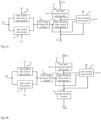
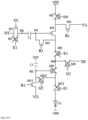
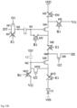
- a pixel driving circuit is provided in some embodiments of the present disclosure, which includes a light-emission time control sub-circuitry 11, a first resetting sub-circuitry 12, a first light-emission control sub-circuitry 13, a time control data write-in sub-circuitry 14, a data control sub-circuitry 15 and a first energy storage sub-circuitry 1.
- the first resetting sub-circuitry 12 is electrically connected to a resetting control line R1, a first initial voltage end, and a first end, a control end and a second end of the light-emission time control sub-circuitry 11, and configured to write a first initial voltage Vil from the first initial voltage end into the first end of the light-emission time control sub-circuitry 11 under the control of a resetting control signal from the resetting control line R1, and control the control end of the light-emission time control sub-circuitry 11 to be electrically connected to the second end of the light-emission time control sub-circuitry 11 under the control of the resetting control signal.
- a first end of the first energy storage sub-circuitry 1 is electrically connected to the control end of the light-emission time control sub-circuitry 11, and the first energy storage sub-circuitry 1 is configured to store a voltage.
- the time control data write-in sub-circuitry 14 is electrically connected to a first gate line G1, a time control data line DT and a second end of the first energy storage sub-circuitry 1, and configured to control the time control data line DT to be electrically connected to the second end of the first energy storage sub-circuitry 1 under the control of a first gate driving signal from the first gate line G1.
- the data control sub-circuitry 15 is electrically connected to a light-emission control line E1, the time control data line DT and the second end of the first energy storage sub-circuitry 1, and configured to control the time control data line DT to be electrically connected to the second end of the first energy storage sub-circuitry 1 under the control of a light-emission control signal from the light-emission control line E1.
- the first light-emission control sub-circuitry 13 is electrically connected to the light-emission control line E1, the first end of the light-emission time control sub-circuitry 11 and a first voltage end Vt1, and configured to control the first end of the light-emission time control sub-circuitry 11 to be electrically connected to the first voltage end Vt1 under the control of the light-emission control signal.
- the second end of the light-emission time control sub-circuitry 11 is electrically connected to an output end U1, and the light-emission time control sub-circuitry 11 is configured to control the first end of the light-emission time control sub-circuitry 11 to be electrically connected to the second end of the light-emission time control sub-circuitry 11 under the control of a potential at the control end of the light-emission time control sub-circuitry 11.
- the pixel driving circuit is configured to drive a light-emitting element, and the output end U1 may be electrically connected to the light-emitting element.
- a luminous brightness value may be determined through controlling a light-emission time of the light-emitting element, so it is able to prevent the occurrence of chromaticity coordinate offset at different currents and unstable brightness at a low current density for the light-emitting element, adjust the luminous brightness value through adjusting the light-emission time of the light-emitting element at a fixed large current density, and compensate for the luminous brightness value when a threshold voltage drift occurs for a transistor due to a low-temperature polycrystalline silicon technology.
- the light-emitting element may be, but not limited to, a micro LED or an Organic Light-Emitting Diode (OLED).
- OLED Organic Light-Emitting Diode
- a voltage applied by the first voltage end Vt1 may be associated with a type of a light-emission time control transistor of the light-emission time control sub-circuitry 11.
- a first voltage applied by the first voltage end Vt1 may be, but not limited to, a voltage of 0V or a negative voltage.
- the first voltage applied by the first voltage end Vt1 may be, but not limited to, a positive voltage.
- the first energy storage sub-circuitry 1 may include, but not limited to, a time control capacitor.
- a light-emitting element 10 is added.
- a first electrode of the light-emitting element 10 may be electrically connected to, but not limited to, the output end U1, and a second electrode of the light-emitting element 10 may receive, but not limited to, a low voltage VSS.
- the first electrode of the light-emitting element 10 may be, but not limited to, an anode, and the second electrode of the light-emitting element 10 may be, but not limited to, a cathode.
- a display period may include a resetting time period, a compensation time period and a light-emission stage.
- the first resetting sub-circuitry 12 may write the first initial voltage Vil into the first end of the light-emission time control sub-circuitry 11 and control the control end of the light-emission time control sub-circuitry 11 to be electrically connected to the second end of the light-emission time control sub-circuitry 11 under the control of the resetting control signal.
- the time control data write-in sub-circuitry 14 may write a predetermined time control data voltage VdT from the time control data line into the second end of the first energy storage sub-circuitry 1 under the control of the first gate driving signal.
- the light-emission time control sub-circuitry 11 may control the first end of the light-emission time control sub-circuitry 11 to be electrically connected to the second end of the light-emission time control sub-circuitry 11 under the control of the control end of the light-emission time control sub-circuitry 11. In this way, it is able to correspondingly change a voltage applied to the first end of the first energy storage sub-circuitry 1 until the light-emission time control sub-circuitry 11 has been turned off.
- the time control data write-in sub-circuitry 14 may write a predetermined voltage V0 from the time control data line DT into the second end of the first energy storage sub-circuitry 1 under the control of the first gate driving signal from the first gate line G1, so as to correspondingly change the voltage applied to the first end of the first energy storage sub-circuitry 1.
- the first light-emission control sub-circuitry 13 may control the first end of the light-emission time control sub-circuitry 11 to be electrically connected to the first voltage end Vt1 under the control of the light-emission control signal
- the data control sub-circuitry 15 may control the time control data line DT to be electrically connected to the second end of the first energy storage sub-circuitry 1 under the control of the light-emission control signal from the light-emission control line E1, so as to correspondingly change the voltage applied to the first end of the first energy storage sub-circuitry 1.
- the light-emission time control sub-circuitry 11 may control the first end of the light-emission time control sub-circuitry 11 to be electrically connected to, or electrically disconnected from, the second end of the light-emission time control sub-circuitry 11 under the control of the voltage applied to the first end of the first energy storage sub-circuitry 1.
- the predetermined voltage V0 may be, but not limited to, 0V. In actual use, V0 may also be a positive or negative voltage, i.e., V0 may be set according to the practical need.
- the light-emission time control sub-circuitry 11 when the light-emission time control sub-circuitry 11 is turned off, it means that the first end and the second end of the light-emission time control sub-circuitry 11 are electrically disconnected from each other.
- the light-emission time control sub-circuitry 11 When the light-emission time control sub-circuitry 11 is turned on, it means that the first end and the second end of the light-emission time control sub-circuitry 11 are electrically connected to each other.
- the time control data voltage applied by DT may change, so as to control the light-emission time control sub-circuitry 11 from an on state to an off state, or from the off state to the on state, thereby to control a light-emission time of the light-emitting element 10.
- the time control data voltage applied by the time control data line is equal to V0-Kt, where t represents a difference between a current time and a start time of the light-emission stage.
- the light-emission time control transistor of the light-emission time control sub-circuitry is a p-type transistor and K is a positive number, or the light-emission time control transistor of the light-emission time control sub-circuitry is an n-type transistor and K is a negative number.
- the time control data voltage may change according to any other rule, so as to control the light-emission time of the light-emitting element.
- the pixel driving circuit may further include a second light-emission control sub-circuitry electrically connected to the light-emission control line, the second end of the light-emission time control sub-circuitry and the output end, and configured to control the second end of the light-emission time control sub-circuitry to be electrically connected to the light-emitting element under the control of the light-emission control signal.
- the pixel driving circuit may further include a second light-emission control sub-circuitry 16 electrically connected to the light-emission control line E1, the second end of the light-emission time control sub-circuitry 11 and the output end U1, and configured to control the second end of the light-emission time control sub-circuitry 11 to be electrically connected to the output end U1 under the control of the light-emission control signal.
- a second light-emission control sub-circuitry 16 electrically connected to the light-emission control line E1, the second end of the light-emission time control sub-circuitry 11 and the output end U1, and configured to control the second end of the light-emission time control sub-circuitry 11 to be electrically connected to the output end U1 under the control of the light-emission control signal.
- the additional second light-emission control sub-circuitry 16 it is able to control the second end of the light-emission time control sub-circuitry 11 to be electrically connected to, or electrically disconnected from, the first electrode of the light-emitting element 10 under the control of the light-emission control signal.
- the light-emitting element 10 when VSS is greater than or equal to Vi1, the light-emitting element 10 may be in a reverse biased state within the resetting time period, and at this time the second light-emission control sub-circuitry 16 may be omitted.
- VSS is smaller than Vi1, it is necessary to provide the second light-emission control sub-circuitry 16.
- the light-emission time control sub-circuitry includes a light-emission time control transistor, a control electrode of which is the control end of the light-emission time control sub-circuitry, a first electrode of which is the first end of the light-emission time control sub-circuitry, and a second electrode of which is the second end of the light-emission time control sub-circuitry.
- the first resetting sub-circuitry includes a first resetting transistor and a second resetting transistor.
- a control electrode of the first resetting transistor is electrically connected to the resetting control line
- a first electrode of the first resetting transistor is electrically connected to the control end of the light-emission time control sub-circuitry
- a second electrode of the first resetting transistor is electrically connected to the second end of the light-emission time control sub-circuitry.
- a control electrode of the second resetting transistor is electrically connected to the resetting control line, a first electrode of the second resetting transistor is electrically connected to the first end of the light-emission time control sub-circuitry, and a second electrode of the second resetting transistor is electrically connected to the first initial voltage end for applying the first initial voltage.
- the time control data write-in sub-circuitry includes a time control data write-in transistor, a control electrode of which is electrically connected to the first gate line, a first electrode of which is electrically connected to the time control data line, and a second electrode of which is electrically connected to the second end of the first energy storage sub-circuitry.
- the data control sub-circuitry includes a data control transistor.
- a control electrode of the data control transistor is electrically connected to the light-emission control line, a first electrode of the data control transistor is electrically connected to the time control data line, and a second electrode of the data control transistor is electrically connected to the second end of the first energy storage sub-circuitry.
- the first light-emission control sub-circuitry includes a first light-emission control transistor, a control electrode of which is electrically connected to the light-emission control line, a first electrode of which is electrically connected to the first voltage end, and a second electrode of which is electrically connected to the first end of the light-emission time control sub-circuitry.
- the second light-emission control sub-circuitry may include a second light-emission control transistor, a control electrode of which is electrically connected to the light-emission control line, a first electrode of which is electrically connected to the second end of the light-emission time control sub-circuitry, and a second electrode of which is electrically connected to the output end.
- the light-emission time control sub-circuitry includes a light-emission time control transistor
- the first resetting sub-circuitry includes a first resetting transistor and a second resetting transistor
- the time control data write-in sub-circuitry includes a time control data write-in transistor
- the data control sub-circuitry includes a data control transistor
- the first light-emission control sub-circuitry includes a first light-emission control transistor
- the first energy storage sub-circuitry includes a time control capacitor.
- a control electrode of the light-emission time control transistor is the control end of the light-emission time control sub-circuitry
- a first electrode of the light-emission time control transistor is the first end of the light-emission time control sub-circuitry
- a second electrode of the light-emission time control transistor is the second end of the light-emission time control sub-circuitry.
- a control electrode of the first resetting transistor is electrically connected to the resetting control line, a first electrode of the first resetting transistor is electrically connected to the control end of the light-emission time control sub-circuitry, and a second electrode of the first resetting transistor is electrically connected to the second end of the light-emission time control sub-circuitry.
- a control electrode of the second resetting transistor is electrically connected to the resetting control line, a first electrode of the second resetting transistor is electrically connected to the first end of the light-emission time control sub-circuitry, and a second electrode of the second resetting transistor is electrically connected to the first initial voltage end for applying the first initial voltage.
- a control electrode of the time control data write-in transistor is electrically connected to the first gate line, a first electrode of the time control data write-in transistor is electrically connected to the time control data line, and a second electrode of the time control data write-in transistor is electrically connected to the second end of the first energy storage sub-circuitry.
- a control electrode of the data control transistor is electrically connected to the light-emission control line, a first electrode of the data control transistor is electrically connected to the time control data line, and a second electrode of the data control transistor is electrically connected to the second end of the first energy storage sub-circuitry.
- a control electrode of the first light-emission control transistor is electrically connected to the light-emission control line, a first electrode of the first light-emission control transistor is electrically connected to the first voltage end, and a second electrode of the first light-emission control transistor is electrically connected to the first end of the light-emission time control sub-circuitry.
- the first end of the first energy storage sub-circuitry is a first end of the time control capacitor, and the second end of the first energy storage sub-circuitry is a second end of the time control capacitor.
- the pixel driving circuit may further include a second light-emission control sub-circuitry
- the second light-emission control sub-circuitry may include a second light-emission control transistor, a control electrode of which is electrically connected to the light-emission control line, a first electrode of which is electrically connected to the second end of the light-emission control sub-circuitry, and a second electrode of which is electrically connected to the output end.
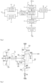
- the pixel driving circuit is configured to drive a micro LED O1, and it may include the light-emission time control sub-circuitry 11, the first resetting sub-circuitry 12, the first light-emission control sub-circuitry 13, the time control data write-in sub-circuitry 14, the data control sub-circuitry 15, the second light-emission control sub-circuitry 16 and the first energy storage sub-circuitry 1.
- the light-emission time control sub-circuitry 11 may include a light-emission time control transistor M4, the first resetting sub-circuitry 12 may include a first resetting transistor M3 and a second resetting transistor M5, the time control data write-in sub-circuitry 14 may include a time control data write-in transistor M1, the data control sub-circuitry 15 may include a data control transistor M7, the first light-emission control sub-circuitry 13 may include a first light-emission control transistor M2, the second light-emission control sub-circuitry 16 may include a second light-emission control transistor M6, and the first energy storage sub-circuitry 1 may include a time control capacitor C1.
- a gate electrode of M3 may be electrically connected to the resetting control line R1, a source electrode of M3 may be electrically connected to a gate electrode of M4, and a drain electrode of M3 may be electrically connected to a drain electrode of M4.
- a gate electrode of M5 may be electrically connected to the resetting control line R1, a source electrode of M5 may be electrically connected to a source electrode of M4, and a drain electrode of M5 may be electrically connected to the first initial voltage end for applying the first initial voltage Vil.
- a gate electrode of M1 may be electrically connected to the first gate line G1, a source electrode of M1 may be electrically connected to the time control data line DT, and a drain electrode of M1 may be electrically connected to a second end of C1.
- a gate electrode of M7 may be electrically connected to the light-emission control line E1, a source electrode of M7 may be electrically connected to the time control data line DT, a drain electrode of M7 may be electrically connected to the second end of C1, and a first end of C1 may be electrically connected to the gate electrode of M4.
- a gate electrode of M2 may be electrically connected to the light-emission control line E1, a source electrode of M2 may receive a first voltage VDD, and a drain electrode of M2 may be electrically connected to the source electrode of M4.
- a gate electrode of M6 may be electrically connected to the light-emission control line E1, a source electrode of M6 may be electrically connected to the drain electrode of M4, a drain electrode of M6 may be electrically connected to an anode of O1, and a cathode of O1 may receive a low voltage VSS.
- all the transistors may be, but not limited to, p-type TFTs.
- N1 may be a first node connected to the gate electrode of M4, and N2 may be a second node connected to the second end of C1.
- Vi1 may be, but not limited to, 0V.
- a value of Vil may be set according to the practical need.
- the anode of O1 may be the first electrode of the light-emitting element, and the cathode of O1 may be the second electrode of the light-emitting element.
- O1 when VSS is greater than or equal to Vi1, O1 may be in a reverse biased state within the resetting time period, and at this time M6 may be omitted.
- VSS is smaller than Vi1, it is necessary to provide M6.
- a display period may include a resetting time period t1, a compensation time period t2 and a light-emission stage te.
- a high level may be applied to E1 so as to turn off M2, M6 and M7, a low level may be applied to R1 and G1 so as to turn on M1, M3, M4 and M5, and the predetermined time control data voltage VdT may be applied to DT, so a voltage of N2 may be equal to VdT and a voltage of the source electrode of M4 may be Vi1.
- M4 may be turned on to change a potential at the gate electrode of M4 until a potential at N1 is Vi1+Vth4, where Vth4 represents a threshold voltage of M4.
- Vi1 may be set as 0V, so the potential at N1 may be Vth4 and a potential at N2 may be VdT.
- a high level may be applied to E1 to turn off M2, M6 and M7, a high level may be applied to R1 to turn off M3 and M5, and a data voltage of 0V may be applied to DT.
- the potential at N2 may jump from VdT to 0V, so the potential at N1 may jump from Vth4 to Vth4-VdT. Under the control of the potential at N1, M4 may be turned off.
- a high level may be applied to G1 to turn off M1
- a high level may be applied to R1 to maintain M3 and M5 to be each in an off state
- a low level may be applied to E1 to turn on M2, M6 and M7.
- Fig.4 shows a waveform of the time control data voltage applied by DT. As shown in Fig.4 , the time control data voltage decreases at a constant slope from the voltage of 0V within the compensation time period t2 until the beginning of a next frame.
- a voltage value of the time control data voltage may be a predetermined voltage.
- VDD may be preferentially set as 0V or less, i.e., Vgs4>Vth4.
- M4 may be turned on.
- M4 may be switched from an off state to an on state, and a turn-on time of M4 may depend on VdT and a value of the time control data voltage within the light-emission stage te, i.e., the turn-on time of M4 may be independent of Vth4.
- M4 may be in a fully on state and at a non-saturated region.
- Id represents a driving current for driving O1 to emit light
- Vn1 represents the voltage of N1.
- a display panel may include the pixel driving circuits arranged in rows and columns.
- one frame F1 may include a preparation stage and the light-emission stage te arranged one after another.
- the preparation stage may include a plurality of preparation time periods arranged one after another, and each preparation time period may include a resetting time period and a compensation time period arranged one after another.
- t1-1 represents a first resetting time period
- t1-2 represents a first compensation time period
- t2-1 represents a second resetting time period
- t2-2 represents a second compensation time period
- tn-1 represents an n th resetting time period
- tn-2 represents an n th compensation time period
- E1 represents the light-emission control line
- DTm represents an m th time control data line
- R11 represents a first resetting control line
- G11 represents a first gate line in a first row
- R12 represents a second resetting control line
- G12 represents a first gate line in a second row
- G1n represents a first gate line in an n th row
- R1n represents an n th resetting control line
- Vn11 represents a potential at a first node N1 in a pixel driving circuit in a first row and an m th column
- Vn12 represents a potential at a first node N1 in
- the pixel driving circuit in the first row and the m th column is configured to drive the micro LED in the first row and the m th column
- the pixel driving circuit in the second row and the m th column is configured to drive the micro LED in the second row and the m th column
- the pixel driving circuit in the n th row and the m th column is configured to drive the micro LED in the n th row and the m th column.
- a first time control data voltage VdT1 may be written into DTm; within t1-2, a voltage of 0V may be written into DTm; within t2-1, a second time control data voltage VdT2 may be written into DTm; within t2-2, a voltage of 0V may be written into DTm; within tn-1, an n th time control data voltage VdTn may be written into DTm; and within tn-2, a voltage of 0V may be written into DTm.
- the data voltage on DTm may decrease at a constant slope from 0V, so as to control the light-emission time of each micro LED.
- the micro LED has been considered as a next-generation display technology due to such characteristics as low driving voltage, ultra-high brightness, long service life and high temperature resistance.
- it is immature to transfer and bind the micro LED, and there is no corresponding glass-based driving back plate, so a micro-LED display panel has not been available in the market so far.
- a scheme for the glass-based driving back plate is presented, and the pixel driving circuit is mainly provided to solve such problems for the micro LED as chromaticity coordinate offset at different currents and unstable brightness at a low current density.
- the pixel driving circuit including the micro LED is arranged on a Printed Circuit Board (PCB) substrate.
- PCB Printed Circuit Board
- the pixel driving circuit may control a grayscale value through controlling the light-emission time at a constant current or constant voltage.
- the threshold voltage drift of the transistor due to the low-temperature polycrystalline silicon technology may be taken into consideration, i.e., the threshold voltage drift may be compensated.
- the light-emission time control transistor M4 may be turned on regardless of the threshold voltage, so it is able to accurately control the light-emission time in accordance with the time control data voltage and provide more grayscale values.
- the turn-on time of M4 and a time when the current flows to the micro LED may be controlled in accordance with the potential at N1, i.e., the brightness value may be determined in accordance with the time when the micro LED emits light within one frame.
- the pixel driving circuit is mainly provided to solve such problems for the micro LED as chromaticity coordinate offset at different currents and unstable brightness at a low current density.
- a new pixel driving circuit for the glass-based micro LED display panel has been presented, so as to control the grayscale values through controlling the light-emission time at a constant current or constant voltage.
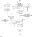
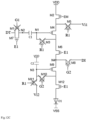
- the pixel driving circuit is configured to drive the light-emitting element 10 to emit light, and it may include a current driving sub-circuitry 70, the light-emission time control sub-circuitry 11, the first energy storage sub-circuitry 1, the first resetting sub-circuitry 12, the first light-emission control sub-circuitry 13, the time control data write-in sub-circuitry 14 and the data control sub-circuitry 15.
- the first resetting sub-circuitry 12 is electrically connected to the resetting control line R1, the first initial voltage end, and the first end, the control end and the second end of the light-emission time control sub-circuitry 11, and configured to write the first initial voltage Vil from the first initial voltage end into the first end of the light-emission time control sub-circuitry 11 under the control of the resetting control signal from the resetting control line R1, and control the control end of the light-emission time control sub-circuitry 11 to be electrically connected to the second end of the light-emission time control sub-circuitry 11 under the control of the resetting control signal.
- the first end of the first energy storage sub-circuitry 1 is electrically connected to the control end of the light-emission time control sub-circuitry 11.
- the time control data write-in sub-circuitry 14 is electrically connected to the first gate line G1, the time control data line DT and the second end of the first energy storage sub-circuitry 1, and configured to control the time control data line DT to be electrically connected to the second end of the first energy storage sub-circuitry 1 under the control of the first gate driving signal from the first gate line G1.
- the data control sub-circuitry 15 is electrically connected to the light-emission control line E1, the time control data line DT and the second end of the first energy storage sub-circuitry 1, and configured to control the time control data line DT to be electrically connected to the second end of the first energy storage sub-circuitry 1 under the control of a light-emission control signal from the light-emission control line E1.
- the first light-emission control sub-circuitry 13 is electrically connected to the light-emission control line E1, the first end of the light-emission time control sub-circuitry 11 and the first voltage end Vt1, and configured to control the first end of the light-emission time control sub-circuitry 11 to be electrically connected to the first voltage end Vt1 under the control of the light-emission control signal.
- the second end of the light-emission time control sub-circuitry 11 is electrically connected to the first electrode of the light-emitting element 10, and the light-emission time control sub-circuitry 11 is configured to control the first end of the light-emission time control sub-circuitry 11 to be electrically connected to the second end of the light-emission time control sub-circuitry 11 under the control of a potential at the control end of the light-emission time control sub-circuitry 11.
- the current driving sub-circuitry 70 is electrically connected to a current control data line DI, connected between the second end of the light-emission time control sub-circuitry 11 and the first electrode of the light-emitting element 10, and configured to generate a driving current for driving the light-emitting element 10 to emit light at the light-emission stage in accordance with the current control data voltage from the current control data line DI.
- the first electrode of the light-emitting element 10 is electrically connected to the output end U1, and the second electrode of the light-emitting element 10 may receive a low voltage VSS.
- the current driving sub-circuitry 70 may control a size of the driving current for driving the light-emitting element 10 to emit light, and the light-emission time control sub-circuitry 11, the first energy storage sub-circuitry 1, the first resetting sub-circuitry 12, the first light-emission control sub-circuitry 13, the time control data write-in sub-circuitry 14 and the data control sub-circuitry 15 may control the light-emission time of the light-emitting element 10.
- the display period may include a resetting time period, a compensation time period and a light-emission stage.
- the first resetting sub-circuitry 12 may write the first initial voltage Vil into the first end of the light-emission time control sub-circuitry 11 and control the control end of the light-emission time control sub-circuitry 11 to be electrically connected to the second end of the light-emission time control sub-circuitry 11 under the control of the resetting control signal.
- the time control data write-in sub-circuitry 14 may write a predetermined time control data voltage VdT from the time control data line into the second end of the first energy storage sub-circuitry 1 under the control of the first gate driving signal.
- the light-emission time control sub-circuitry 11 may control the first end of the light-emission time control sub-circuitry 11 to be electrically connected to the second end of the light-emission time control sub-circuitry 11 under the control of the control end of the light-emission time control sub-circuitry 11. In this way, it is able to correspondingly change a voltage applied to the first end of the first energy storage sub-circuitry 1 until the light-emission time control sub-circuitry 11 has been turned off.
- the time control data write-in sub-circuitry 14 may write a predetermined voltage V0 from the time control data line DT into the second end of the first energy storage sub-circuitry 1 under the control of the first gate driving signal from the first gate line G1, so as to correspondingly change the voltage applied to the first end of the first energy storage sub-circuitry 1.
- the current driving sub-circuitry 70 may generate the driving current for driving the light-emitting element 10 to emit light in accordance with the current control data voltage across the current control data line DI
- the first light-emission control sub-circuitry 13 may control the first end of the light-emission time control sub-circuitry 11 to be electrically connected to the first voltage end Vt1 under the control of the light-emission control signal
- the data control sub-circuitry 15 may control the time control data line DT to be electrically connected to the second end of the first energy storage sub-circuitry 1 under the control of the light-emission control signal from the light-emission control line E1, so as to correspondingly change the voltage applied to the first end of the first energy storage sub-circuitry 1.
- the light-emission time control sub-circuitry 11 may control the first end of the light-emission time control sub-circuitry 11 to be electrically connected to, or electrically disconnected from, the second end of the light-emission time control sub-circuitry 11 under the control of the voltage applied to the first end of the first energy storage sub-circuitry 1.
- the current driving sub-circuitry may include a driving sub-circuitry, a current control data write-in sub-circuitry, a second resetting sub-circuitry, a compensation sub-circuitry and a second energy storage sub-circuitry.
- a first end of the driving sub-circuitry may be electrically connected to the second end of the light-emission time control sub-circuitry, a second end of the driving sub-circuitry may be electrically connected to the output end, and the driving sub-circuitry is configured to control the first end of the driving sub-circuitry to be electrically connected to the second end of the driving sub-circuitry under the control of a potential at a control end of the driving sub-circuitry.
- a first end of the second energy storage sub-circuitry may be electrically connected to the control end of the driving sub-circuitry, a second end of the second energy storage sub-circuitry may be electrically connected to a second voltage end, and the second energy storage sub-circuitry is configured to store a voltage.
- the current control data write-in sub-circuitry may be electrically connected to a second gate line, the current control data line and the first end of the driving sub-circuitry, and configured to control the current control data line to be electrically connected to the first end of the driving sub-circuitry under the control of a second gate driving signal from the second gate line.
- the second resetting sub-circuitry may be electrically connected to the resetting control line, a second initial voltage end and the control end of the driving sub-circuitry, and configured to apply a second initial voltage from the second initial voltage end to the control end of the driving sub-circuitry under the control of the resetting control signal from the resetting control line.
- the compensation sub-circuitry may be electrically connected to the second gate line, the control end of the driving sub-circuitry and the second end of the driving sub-circuitry, and configured to control the control end of the driving sub-circuitry to be electrically connected to the second end of the driving sub-circuitry under the control of the second gate driving signal.
- the first energy storage sub-circuitry may include a time control capacitor
- the second energy storage sub-circuitry may include a current control capacitor
- the current driving sub-circuitry may include a driving sub-circuitry 71, a current control data write-in sub-circuitry 72, a second resetting sub-circuitry 73, a compensation sub-circuitry 74 and a second energy storage sub-circuitry 70.
- a first end of the driving sub-circuitry 71 may be electrically connected to the second end of the light-emission time control sub-circuitry 11, a second end of the driving sub-circuitry 71 may be electrically connected to the first electrode of the light-emitting element 10, and the driving sub-circuitry 71 is configured to control the first end of the driving sub-circuitry 71 to be electrically connected to the second end of the driving sub-circuitry 71 under the control of a potential at a control end of the driving sub-circuitry 71.
- a first end of the second energy storage sub-circuitry 70 may be electrically connected to the control end of the driving sub-circuitry 71, a second end of the second energy storage sub-circuitry 70 may be electrically connected to a second voltage end Vt2.
- the current control data write-in sub-circuitry 72 may be electrically connected to a second gate line G2, the current control data line DI and the first end of the driving sub-circuitry 71, and configured to control the current control data line DI to be electrically connected to the first end of the driving sub-circuitry 71 under the control of a second gate driving signal from the second gate line G2.
- the second resetting sub-circuitry 73 may be electrically connected to the resetting control line R1, a second initial voltage end and the control end of the driving sub-circuitry 71, and configured to apply a second initial voltage Vi2 from the second initial voltage end to the control end of the driving sub-circuitry under the control of the resetting control signal from the resetting control line R1.
- the compensation sub-circuitry 74 may be electrically connected to the second gate line G2, the control end of the driving sub-circuitry 71 and the second end of the driving sub-circuitry 71, and configured to control the control end of the driving sub-circuitry 71 to be electrically connected to the second end of the driving sub-circuitry 71 under the control of the second gate driving signal.
- the second voltage end may be, but limited to, the same as the first voltage end. In actual use, the second voltage end may also be different from the first voltage end.
- the second resetting sub-circuitry 73 may apply the second initial voltage Vi2 to the control end of the driving sub-circuitry 71 under the control of the resetting control signal, so as to enable the first end and the second end of the driving sub-circuitry 71 to be electrically disconnected from each other under the control of the potential at the control end of the driving sub-circuitry 71.
- the current control data write-in sub-circuitry 72 may write the predetermined current control data voltage VdI from the current control data line DI into the first end of the driving sub-circuitry 71 under the control of the second gate driving signal from the second gate line G2.
- the compensation sub-circuitry 74 may control the control end of the driving sub-circuitry 71 to be electrically connected to the second end of the driving sub-circuitry 71 under the control of the second gate driving signal, so as to enable the first end and the second end of the driving sub-circuitry 71 to be electrically connected to each other under the control of the potential at the content end of the driving sub-circuitry 71, thereby to correspondingly change the potential at the control end of the driving sub-circuitry 71 until the driving sub-circuitry 71 has been turned off.
- the driving sub-circuitry 71 may generate the driving current under the control of the potential at the control end of the driving sub-circuitry 71, so as to drive the light-emitting element 10 to emit light.
- the pixel driving circuit may further include a second light-emission control sub-circuitry through which the first end of the driving sub-circuitry is electrically connected to the second end of the light-emission time control sub-circuitry.
- a control end of the second light-emission control sub-circuitry may be electrically connected to the light-emission control line, a first end of the second light-emission control sub-circuitry may be electrically connected to the second end of the light-emission time control sub-circuitry, and a second end of the second light-emission control sub-circuitry may be electrically connected to the driving sub-circuitry.
- the second light-emission control sub-circuitry is configured to control the second end of the light-emission time control sub-circuitry to be electrically connected to the driving sub-circuitry under the control of the light-emission control signal from the light-emission control line.
- the pixel driving circuit may further include a third light-emission control sub-circuitry through which the second end of the driving sub-circuitry is electrically connected to the output end.
- the third light-emission control sub-circuitry is configured to control the second end of the driving sub-circuitry to be electrically connected to the output end under the control of the light-emission control signal from the light-emission control line.
- the pixel driving circuit may further include a second light-emission control sub-circuitry 16 and a third light-emission control sub-circuitry 75.
- the first end of the driving sub-circuitry 71 may be electrically connected to the second end of the light-emission time control sub-circuitry 11 through the second light-emission control sub-circuitry 16.
- a control end of the second light-emission control sub-circuitry 16 may be electrically connected to the light-emission control line E1
- a first end of the second light-emission control sub-circuitry 16 may be electrically connected to the second end of the light-emission time control sub-circuitry 11
- a second end of the second light-emission control sub-circuitry 16 may be electrically connected to the first end of the driving sub-circuitry 71.
- the second light-emission control sub-circuitry 16 is configured to control the second end of the light-emission time control sub-circuitry 11 to be electrically connected to first end of the driving sub-circuitry 71 under the control of the light-emission control signal from the light-emission control line E1.
- the second end of the driving sub-circuitry 71 may be electrically connected to the first electrode of the light-emitting element 10 through the third light-emission control sub-circuitry 75.
- the second electrode of the light-emitting element 10 may receive the low voltage VSS, and the first electrode of the light-emitting element 10 may be electrically connected to the output end U1.
- the third light-emission control sub-circuitry 75 may be electrically connected to the light-emission control line E1, and the third light-emission control sub-circuitry is configured to control the second end of the driving sub-circuitry 71 to be electrically connected to the first electrode of the light-emitting element 10 under the control of the light-emission control signal from the light-emission control line E1.
- the second light-emission control sub-circuitry 16 may control the first end and the second end of the second light-emission control sub-circuitry 16 to be electrically connected to each other under the control of the light-emission control signal, and the third light-emission control sub-circuitry 75 may control the second end of the driving sub-circuitry 71 to be electrically connected to the first electrode of the light-emitting element 10.
- the second energy storage sub-circuitry may include a current control capacitor.
- the first end of the second energy storage sub-circuitry may be, but not limited to, a first end of the current control capacitor, and the second end of the second energy storage sub-circuitry may be, but not limited to, a second end of the current control capacitor.
- the driving sub-circuitry may include a driving transistor, a control electrode of which is electrically connected to the first end of the current control capacitor, a first electrode of which is electrically connected to the second end of the light-emission time control sub-circuitry, and a second electrode of which is electrically connected to the output end.
- the current control data write-in sub-circuitry may include a current control data write-in transistor, a control electrode of which is electrically connected to the second gate line, a first electrode of which is electrically connected to the current control data line, and a second electrode of which is electrically connected to the first end of the driving sub-circuitry.
- the second resetting sub-circuitry may include a third resetting transistor, a control electrode of which is electrically connected to the resetting control line, a first electrode of which is electrically connected to the second initial voltage end, and a second electrode of which is electrically connected to the control end of the driving sub-circuitry.
- the compensation sub-circuitry may include a compensation transistor, a control electrode of which is electrically connected to the second gate line, a first electrode of which is electrically connected to the control end of the driving sub-circuitry, and a second electrode of which is electrically connected to the second end of the driving sub-circuitry.
- the third light-emission control sub-circuitry may include a third light-emission control transistor, a control electrode of which is electrically connected to the light-emission control line, a first electrode of which is electrically connected to the second end of the driving sub-circuitry, and a second electrode of which is electrically connected to the output end.
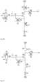
- the pixel driving circuit is configured to drive the micro LED O1 to emit light, and it may include a current driving sub-circuitry, the light-emission time control sub-circuitry 11, the first energy storage sub-circuitry 1, the first resetting sub-circuitry 12, the first light-emission control sub-circuitry 13, the time control data write-in sub-circuitry 14, the data control sub-circuitry 15 and the second light-emission control sub-circuitry 16.
- the light-emission time control sub-circuitry 11 may include a light-emission time control transistor M4, the first resetting sub-circuitry 12 may include a first resetting transistor M3 and a second resetting transistor M5, the time control data write-in sub-circuitry 14 may include a time control data write-in transistor M1, the data control sub-circuitry 15 may include a data control transistor M7, the first light-emission control sub-circuitry 13 may include a first light-emission control transistor M2, the second light-emission control sub-circuitry 16 may include a second light-emission control transistor M6, and the first energy storage sub-circuitry 1 may include a time control capacitor C1.
- a gate electrode of M3 may be electrically connected to the resetting control line R1, a source electrode of M3 may be electrically connected to a gate electrode of M4, and a drain electrode of M3 may be electrically connected to a drain electrode of M4.
- a gate electrode of M5 may be electrically connected to the resetting control line R1, a source electrode of M5 may be electrically connected to a source electrode of M4, and a drain electrode of M5 may be electrically connected to the first initial voltage end for applying the first initial voltage Vil.
- a gate electrode of M1 may be electrically connected to the first gate line G1, a source electrode of M1 may be electrically connected to the time control data line DT, a drain electrode of M1 may be electrically connected to a second end of C1, and a first end of C1 may be electrically connected to the gate electrode of M4.
- a gate electrode of M7 may be electrically connected to the light-emission control line E1, a source electrode of M7 may be electrically connected to the time control data line DT, and a drain electrode of M7 may be electrically connected to the second end of C1.
- a gate electrode of M2 may be electrically connected to the light-emission control line E1, a source electrode of M2 may receive a first voltage VDD, and a drain electrode of M2 may be electrically connected to the source electrode of M4.
- a gate electrode of M6 may be electrically connected to the light-emission control line E1, a source electrode of M6 may be electrically connected to the drain electrode of M4, and a cathode of O1 may receive a low voltage VSS.
- the current driving sub-circuitry may include a driving sub-circuitry 71, a current control data write-in sub-circuitry 72, a second resetting sub-circuitry 73, a compensation sub-circuitry 74, a third light-emission control sub-circuitry 75 and a second energy storage sub-circuitry 70.
- the second energy storage sub-circuitry 70 may include a current control capacitor C2.
- the driving sub-circuitry 71 may include a driving transistor M9, a gate electrode of which is electrically connected to a first end of C2, and a source electrode of which is electrically connected to the drain electrode of M6.
- the current control data write-in sub-circuitry 72 may include a current control data write-in transistor M8, a gate electrode of which is electrically connected to the second gate line G2, a source electrode of which is electrically connected to the current control data line DI, and a drain electrode of which is electrically connected to a source electrode of M9.
- the second resetting sub-circuitry 73 may include a third resetting transistor M11, a gate electrode of which is electrically connected to the resetting control line R1, a source electrode of which is electrically connected to the second initial voltage end, and a drain electrode of which is electrically connected to the gate electrode of M9.
- the second initial voltage end is configured to apply the second initial voltage Vi2.
- the compensation sub-circuitry 74 may include a compensation transistor M10, a gate electrode of which is electrically connected to the second gate line G2, a source electrode of which is electrically connected to the gate electrode of M9, and a drain electrode of which is electrically connected to a drain electrode of M9.
- the third light-emission control sub-circuitry 75 may include a third light-emission control transistor M12, a gate electrode of which is electrically connected to the light-emission control line E1, a source electrode of which is electrically connected to the drain electrode of M9, and a drain electrode of which is electrically connected to an anode of the micro LED O1.
- the first end of C2 may be electrically connected to the gate electrode of M9, and a second end of C2 may receive the first voltage VDD.
- all the transistors may be, but not limited to, p-type TFTs, and the first voltage end may be, but not limited to, the same as the second voltage end.
- N1 represents a first node electrically connected to the gate electrode of M4, N2 represents a second node electrically connected to the second end of C1, N3 represents a third node electrically connected to the gate electrode of M9, and N4 represents a fourth node electrically connected to the source electrode of M9.
- M6 may be omitted.
- M12 when VdI is smaller than or equal to VSS, M12 may be omitted, and when VdI is greater than VSS, M12 may not be omitted.
- a display period may include a resetting time period t1, a compensation time period t2 and a light-emission stage te.
- a high level may be applied to E1 so as to turn off M2, M6, M7, M8, M9, M11 and M12, a low level may be applied to R1 and G1 so as to turn on M1, M3, M4, M5 and M11, and the predetermined time control data voltage VdT may be applied to DT, so a voltage of N2 may be equal to VdT and a voltage of the source electrode of M4 may be Vi1.
- M4 may be turned on to change the potential at the gate electrode of M4 until a potential at N1 is Vi1+Vth4, where Vth4 represents a threshold voltage of M4.
- Vi1 may be set as 0V
- the potential at N1 may be Vth4 and a potential at N2 may be VdT.
- a voltage of N3 may be Vi2, and Vi2 may also be set as 0V.
- a high level may be applied to E1 to turn off M2, M6 and M7, a high level may be applied to R1 to turn off M3, M5 and M11, and a data voltage of 0V may be applied to DT.
- the potential at N2 may jump from VdT to 0V, so the potential at N1 may jump from Vth4 to Vth4-VdT.
- a low level may be applied to G2 so as to turn on M8 and M10.
- M9 may be turned on, so as to change the voltage of N3 until M9 is turned off. At this time, the voltage of N3 may be maintained as VdI+Vth0 due to the effect of C2, where Vth9 represents a threshold voltage of M9.
- a high level may be applied to G1 and G2 to turn off M1, M8 and M10, a high level may be applied to R1 to maintain M3, M5 and M11 to be each in an off state, and a low level may be applied to E1 to turn on M2, M6, M7 and M12.
- Fig.11 shows a waveform of the time control data voltage applied by DT. As shown in Fig.11 , the time control data voltage decreases at a constant slope from the voltage of 0V until the beginning of a next frame. A voltage value of the time control data voltage may be a predetermined voltage.
- M4 may be turned on.
- a turn-on time of M4 may depend on VdT, i.e., it may be independent of the threshold voltage of M4.
- M9 is a driving transistor for generating a current.
- M9 may be at a saturation region.
- M9 may generate the driving current, and M4 may control the light-emission time.
- M4 may control the light-emission time.
- it is able to provide more grayscale values.
- it is able to compensate for the threshold voltage drift, thereby to prevent a display effect from being adversely effected by the threshold voltage drift of M4 and the threshold voltage drift of M9 due to the low-temperature polycrystalline silicon technology.
- Vn1 represents a voltage of N1
- Vn4 represents a voltage of N4.
- Vn4 may be equal to a difference between the potential at N3 and Vth4.
- the pixel driving circuit is configured to drive the light-emitting element.
- the output end may be electrically connected to the first electrode of the light-emitting element, and the second electrode of the light-emitting element may be electrically connected to a third voltage end.
- the third voltage end may be, but not limited to, a low voltage end.
- a display panel may include the pixel driving circuits arranged in rows and columns.
- one frame may include a preparation stage and the light-emission stage te arranged one after another.
- the preparation stage may include a plurality of preparation time periods arranged one after another, and each preparation time period may include a resetting time period and a compensation time period arranged one after another.
- F1 represents one frame
- t1-1 represents a first resetting time period
- t1-2 represents a first compensation time period
- t2-1 represents a second resetting time period
- t2-2 represents a second compensation time period
- tn-1 represents an n th resetting time period
- tn-2 represents an n th compensation time period
- E1 represents the light-emission control line
- DTm represents an m th time control data line
- R11 represents a first resetting control line
- G11 represents a first gate line in a first row
- R12 represents a second resetting control line
- G12 represents a first gate line in a second row
- G1n represents a first gate line in an n th row
- G21 represents a second gate line in the first row
- G22 represents a second gate line in the second row
- G2n represents a second gate line in the n th row
- R1n represents an n th resetting control line
- Vn11 represents a potential at a first node N1 in a pixel driving circuit in the first row and the m th column
- Vn12 represents a potential at a first node N1 in a pixel driving circuit in the second row and the m th column.
- a first time control data voltage VdT1 may be written into DTm; within t1-2, a voltage of 0V may be written into DTm; within t2-1, a second time control data voltage VdT2 may be written into DTm; within t2-2, a voltage of 0V may be written into DTm; within tn-1, an n th time control data voltage VdTn may be written into DTm; and within tn-2, a voltage of 0V may be written into DTm.
- the data voltage on DTm may decrease at a constant slope from 0V, so as to control the light-emission time of micro LED in each row.
- a method of driving the above-mentioned pixel driving circuit is further provided in some embodiments of the present disclosure, which includes: applying an ON signal to the resetting control line and the first gate line, so as to write a first initial voltage Vi1 into the first end of the light-emission time control sub-circuitry, enable the control end of the light-emission time control sub-circuitry to be electrically connected to the second end of the light-emission time control sub-circuitry, write a predetermined time control data voltage VdT from the time control data line into the second end of the first energy storage sub-circuitry, and enable the first end of the light-emission time control sub-circuitry to be electrically connected to the second end of the light-emission time control sub-circuitry, thereby to change a voltage applied to the first end of the first energy storage sub-circuitry until the light-emission time control sub-circuitry has been turned off; applying an ON signal to the first gate line, so as to write a predetermined voltage V0 from the time
- a luminous brightness value may be determined through controlling a light-emission time of the light-emitting element, so it is able to prevent the occurrence of chromaticity coordinate offset at different currents and unstable brightness at a low current density for the light-emitting element, adjust the luminous brightness value through adjusting the light-emission time of the light-emitting element at a fixed large current density, and compensate for the luminous brightness value when a threshold voltage drift occurs for a transistor due to a low-temperature polycrystalline silicon technology.
- the ON signal may be a signal capable of controlling a corresponding sub-circuitry to be in an on state.
- the ON signal may be a high voltage signal
- the transistor in the sub-circuitry is a p-type transistor
- the ON signal may be a low voltage signal.
- the present disclosure shall not be limited thereto.
- the data voltage applied by the time control data line may be equal to V0-Kt, where t represents a duration of the light-emission stage.
- K may be a positive number
- K may be a negative number
- the pixel driving circuit further includes a current driving sub-circuitry.
- the method further includes, when applying the ON signal to the light-emission control line, generating, by the current driving sub-circuitry, a driving current to be outputted to the output end in accordance with a current control data voltage from the current control data line.
- the current driving sub-circuitry may control a size of the driving current for driving the light-emitting element to emit light
- the other sub-circuitries of the pixel driving circuit may control the light-emission time of the light-emitting element.
- the luminous brightness may be adjusted through adjusting the driving current and the light-emission time simultaneously.
- various grayscale values may be provided through driving the micro LED by a current at the high current density and driving the micro LED by a large current at a low current density, in combination with the adjustment of the light-emission time.
- the current driving sub-circuitry may include a driving sub-circuitry, a current control data write-in sub-circuitry, a second resetting sub-circuitry, a compensation sub-circuitry and a second energy storage sub-circuitry, and the output end is electrically connected to a light-emitting element.
- the method may further include: when applying the ON signal to the resetting control line and the first gate line, writing a second initial voltage into a control end of the driving sub-circuitry, so as to enable a first end of the driving sub-circuitry to be electrically disconnected from a second end of the driving sub-circuitry; when applying the ON signal to the first gate line, applying an ON signal to a second gate line, so as to write the predetermined current control data voltage VdT from the current control data line into the first end of the driving sub-circuitry, and enable the control end of the driving sub-circuitry to be electrically connected to the second end of the driving sub-circuitry, thereby to change a potential at the control end of the driving sub-circuitry until the driving sub-circuitry has been turned off; and when applying the ON signal to the light-emission control line, generating, by the driving sub-circuitry, a driving current for driving the light-emitting element to emit light.
- a display device including the above-mentioned pixel driving circuit is further provided in some embodiments of the present disclosure.
- the display device may be any product or member having a display function, e.g., a mobile phone, a flat-panel computer, a television, a display, a laptop computer, a digital photo frame or a navigator.
- a display function e.g., a mobile phone, a flat-panel computer, a television, a display, a laptop computer, a digital photo frame or a navigator.
Landscapes
- Engineering & Computer Science (AREA)
- Physics & Mathematics (AREA)
- Computer Hardware Design (AREA)
- General Physics & Mathematics (AREA)
- Theoretical Computer Science (AREA)
- Control Of Indicators Other Than Cathode Ray Tubes (AREA)
- Control Of El Displays (AREA)
- Led Devices (AREA)
- Electroluminescent Light Sources (AREA)
- Transforming Electric Information Into Light Information (AREA)
Claims (15)
- Circuit d'attaque de pixel, comprenant un sous-circuit de commande de temps d'émission de lumière (11), un premier sous-circuit de stockage d'énergie (1), un premier sous-circuit de réinitialisation (12), un premier sous-circuit de commande d'émission de lumière (13), un sous-circuit d'écriture de données de commande de temps (14) et un sous-circuit de commande de données (15), dans lequelle premier sous-circuit de réinitialisation (12) est électriquement connecté à une ligne de commande de réinitialisation (R1), une première extrémité de tension initiale et une première extrémité, une extrémité de commande et une seconde extrémité du sous-circuit de commande de temps d'émission de lumière (11), et configuré pour écrire une première tension initiale (Vil) à partir de la première extrémité de tension initiale dans la première extrémité du sous-circuit de commande de temps d'émission de lumière (11) sous la commande d'un signal de commande de réinitialisation provenant de la ligne de commande de réinitialisation (R1), et commander l'extrémité de commande du sous-circuit de commande de temps d'émission de lumière (11) pour être électriquement connecté à la seconde extrémité du sous-circuit de commande de temps d'émission de lumière (11) sous la commande du signal de commande de réinitialisation ;une première extrémité du premier sous-circuit de stockage d'énergie (1) est électriquement connectée à l'extrémité de commande du sous-circuit de commande de temps d'émission de lumière (11), et le premier sous-circuit de stockage d'énergie (1) est configuré pour stocker une tension ;le sous-circuit d'écriture de données de commande de temps (14) est électriquement connecté à une première ligne de grille (G1), une ligne de données de commande de temps (DT) et une seconde extrémité du premier sous-circuit de stockage d'énergie (1), et configuré pour commander la ligne de données de commande de temps (DT) pour être électriquement connecté à la seconde extrémité du premier sous-circuit de stockage d'énergie (1) sous la commande d'un premier signal d'attaque de grille provenant de la première ligne de grille (G1) ;le sous-circuit de commande de données (15) est électriquement connecté à une ligne de commande d'émission de lumière (E1), la ligne de données de commande de temps (DT) et la seconde extrémité du premier sous-circuit de stockage d'énergie (1), et configuré pour commander la ligne de données de commande de temps (DT) pour être électriquement connecté à la seconde extrémité du premier sous-circuit de stockage d'énergie (1) sous la commande d'un signal de commande d'émission de lumière provenant de la ligne de commande d'émission de lumière (E1) ;le premier sous-circuit de commande d'émission de lumière (13) est électriquement connecté à la ligne de commande d'émission de lumière (E1), la première extrémité du sous-circuit de commande de temps d'émission de lumière (11) et une première extrémité de tension (Vt1), et configuré pour commander la première extrémité du sous-circuit de commande de temps d'émission de lumière (11) pour être électriquement connecté à la première extrémité de tension (Vt1) sous la commande du signal de commande d'émission de lumière ; etla seconde extrémité du sous-circuit de commande de temps d'émission de lumière (11) est électriquement connectée à une extrémité de sortie (U1), et le sous-circuit de commande de temps d'émission de lumière (11) est configuré pour commander la première extrémité du sous-circuit de commande de temps d'émission de lumière (11) pour être électriquement connecté à la seconde extrémité du sous-circuit de commande de temps d'émission de lumière (11) sous la commande d'un potentiel à l'extrémité de commande du sous-circuit de commande de temps d'émission de lumière (11) ;dans lequel le sous-circuit de commande de temps d'émission de lumière (11) comprend un transistor de commande de temps d'émission de lumière (M4), le premier sous-circuit de réinitialisation (12) comprend un premier transistor de réinitialisation (M3) et un deuxième transistor de réinitialisation (M5), le sous-circuit d'écriture de données de commande de temps (14) comprend un transistor d'écriture de données de commande de temps (M1), le sous-circuit de commande de données (15) comprend un transistor de commande de données (M7), le premier sous-circuit de commande d'émission de lumière (13) comprend un premier transistor de commande d'émission de lumière (M2), et le premier sous-circuit de stockage d'énergie (1) comprend un condensateur de commande de temps (C1) ;une électrode de commande du transistor de commande de temps d'émission de lumière (M4) est l'extrémité de commande du sous-circuit de commande de temps d'émission de lumière (11), une première électrode du transistor de commande de temps d'émission de lumière (M4) est la première extrémité du sous-circuit de commande de temps d'émission de lumière (11), et une seconde électrode du transistor de commande de temps d'émission de lumière (M4) est la seconde extrémité du sous-circuit de commande de temps d'émission de lumière (11) ;une électrode de commande du premier transistor de réinitialisation (M3) est électriquement connectée à la ligne de commande de réinitialisation (R1), une première électrode du premier transistor de réinitialisation (M3) est électriquement connectée à l'extrémité de commande du sous-circuit de commande de temps d'émission de lumière (11), et une seconde électrode du premier transistor de réinitialisation (M3) est électriquement connectée à la seconde extrémité du sous-circuit de commande de temps d'émission de lumière (11) ;une électrode de commande du deuxième transistor de réinitialisation (M5) est électriquement connectée à la ligne de commande de réinitialisation (R1), une première électrode du deuxième transistor de réinitialisation (M5) est électriquement connectée à la première extrémité du sous-circuit de commande de temps d'émission de lumière (11), et une seconde électrode du deuxième transistor de réinitialisation (M5) est électriquement connectée à la première extrémité de tension initiale pour appliquer la première tension initiale (Vi1) ;une électrode de commande du transistor d'écriture de données de commande de temps (M1) est électriquement connectée à la première ligne de grille (G1), une première électrode du transistor d'écriture de données de commande de temps (M1) est électriquement connectée à la ligne de données de commande de temps (DT), et une seconde électrode du transistor d'écriture de données de commande de temps (M1) est électriquement connectée à la seconde extrémité du premier sous-circuit de stockage d'énergie (1) ;une électrode de commande du transistor de commande de données (M7) est électriquement connectée à la ligne de commande d'émission de lumière (E1), une première électrode du transistor de commande de données (M7) est électriquement connectée à la ligne de données de commande de temps (DT), et une seconde électrode du transistor de commande de données (M7) est électriquement connectée à la seconde extrémité du premier sous-circuit de stockage d'énergie (1) ;une électrode de commande du premier transistor de commande d'émission de lumière (M2) est électriquement connectée à la ligne de commande d'émission de lumière (E1), une première électrode du premier transistor de commande d'émission de lumière (M2) est électriquement connectée à la première extrémité de tension (Vt1), et une seconde électrode du premier transistor de commande d'émission de lumière (M2) est électriquement connectée à la première extrémité du sous-circuit de commande de temps d'émission de lumière (11) ; etla première extrémité du premier sous-circuit de stockage d'énergie (1) est une première extrémité du condensateur de commande de temps (C1), et la seconde extrémité du premier sous-circuit de stockage d'énergie (1) est une seconde extrémité du condensateur de commande de temps (C1) ;dans lequel le circuit d'attaque de pixel est configuré pour attaquer un élément électroluminescent (10), l'extrémité de sortie (U1) est électriquement connectée à une première électrode de l'élément électroluminescent (10), et une seconde électrode de l'élément électroluminescent (10) est électriquement connectée à une troisième extrémité de tension ;dans lequel le circuit d'attaque de pixel comprend en outre un sous-circuit d'attaque de courant (70) connecté entre la seconde extrémité du sous-circuit de commande de temps d'émission de lumière (11) et l'extrémité de sortie (U1), électriquement connecté à une ligne de données de commande de courant (DI) et à l'extrémité de sortie (U1), et configuré pour générer un courant d'attaque à délivrer à l'extrémité de sortie (U1) lors d'une phase d'émission de lumière en fonction d'une tension de données de commande de courant provenant de la ligne de données de commande de courant (DI).
- Circuit d'attaque de pixel selon la revendication 1, comprenant en outre un deuxième sous-circuit de commande d'émission de lumière (16) électriquement connecté à la ligne de commande d'émission de lumière (E1), la seconde extrémité du sous-circuit de commande de temps d'émission de lumière (11) et l'extrémité de sortie (U1), et configuré pour commander la seconde extrémité du sous-circuit de commande de temps d'émission de lumière (11) pour être électriquement connecté à l'extrémité de sortie (U1) sous la commande du signal de commande d'émission de lumière.
- Circuit d'attaque de pixel selon la revendication 1 ou 2, dans lequel le deuxième sous-circuit de commande d'émission de lumière (16) comprend un deuxième transistor de commande d'émission de lumière, dont une électrode de commande est électriquement connectée à la ligne de commande d'émission de lumière (E1), dont une première électrode est électriquement connectée à la seconde extrémité du sous-circuit de commande de temps d'émission de lumière (11), et dont une seconde électrode est électriquement connectée à l'extrémité de sortie (U1).
- Circuit d'attaque de pixel selon la revendication 1, dans lequel le sous-circuit d'attaque de courant (70) comprend un sous-circuit d'attaque (71), un sous-circuit d'écriture de données de commande de courant (72), un second sous-circuit de réinitialisation (73), un sous-circuit de compensation (74) et un second sous-circuit de stockage d'énergie ; une première extrémité du sous-circuit d'attaque (71) est électriquement connectée à la seconde extrémité du sous-circuit de commande de temps d'émission de lumière (11), une seconde extrémité du sous-circuit d'attaque (71) est électriquement connectée à l'extrémité de sortie (U1), et le sous-circuit d'attaque (71) est configuré pour commander la première extrémité du sous-circuit d'attaque (71) pour être électriquement connecté à la seconde extrémité du sous-circuit d'attaque (71) sous la commande d'un potentiel à une extrémité de commande du sous-circuit d'attaque (71) ; une première extrémité du second sous-circuit de stockage d'énergie est électriquement connectée à l'extrémité de commande du sous-circuit d'attaque (71), une seconde extrémité du second sous-circuit de stockage d'énergie est électriquement connectée à une deuxième extrémité de tension (Vt2), et le second sous-circuit de stockage d'énergie est configuré pour stocker une tension ; le sous-circuit d'écriture de données de commande de courant (72) est électriquement connecté à une seconde ligne de grille (G2), la ligne de données de commande de courant (DI) et la première extrémité du sous-circuit d'attaque (71), et configuré pour commander la ligne de données de commande de courant (DI) pour être électriquement connecté à la première extrémité du sous-circuit d'attaque (71) sous la commande d'un second signal d'attaque de grille provenant de la seconde ligne de grille (G2) ; le second sous-circuit de réinitialisation (73) est électriquement connecté à la ligne de commande de réinitialisation (R1), une deuxième extrémité de tension initiale et l'extrémité de commande du sous-circuit l'attaque (71), et configuré pour appliquer une seconde tension initiale (Vi2) à partir de la deuxième extrémité de tension initiale à l'extrémité de commande du sous-circuit d'attaque (71) sous la commande du signal de commande de réinitialisation provenant de la ligne de commande de réinitialisation (R1) ; et le sous-circuit de compensation (74) est électriquement connecté à la seconde ligne de grille (G2), l'extrémité de commande du sous-circuit d'attaque (71) et la seconde extrémité du sous-circuit d'attaque (71), et configuré pour commander l'extrémité de commande du sous-circuit d'attaque (71) pour être électriquement connecté à la seconde extrémité du sous-circuit d'attaque (71) sous la commande du second signal d'attaque de grille.
- Circuit d'attaque de pixel selon la revendication 4, comprenant en outre un deuxième sous-circuit de commande d'émission de lumière (16) par l'intermédiaire duquel la première extrémité du sous-circuit d'attaque (71) est électriquement connectée à la seconde extrémité du sous-circuit de commande de temps d'émission de lumière (11), dans lequel une extrémité de commande du deuxième sous-circuit de commande d'émission de lumière (16) est électriquement connectée à la ligne de commande d'émission de lumière (E1), une première extrémité du deuxième sous-circuit de commande d'émission de lumière (16) est électriquement connectée à la seconde extrémité du sous-circuit de commande de temps d'émission de lumière (11), et une seconde extrémité du deuxième sous-circuit de commande d'émission de lumière (16) est électriquement connectée au sous-circuit d'attaque (71), et le deuxième sous-circuit de commande d'émission de lumière (16) est configuré pour commander la seconde extrémité du sous-circuit de commande de temps d'émission de lumière (11) pour être électriquement connecté au sous-circuit d'attaque (71) sous la commande du signal de commande d'émission de lumière provenant de la ligne de commande d'émission de lumière (E1).
- Circuit d'attaque de pixel selon la revendication 4, comprenant en outre un troisième sous-circuit de commande d'émission de lumière (75) par l'intermédiaire duquel la seconde extrémité du sous-circuit d'attaque (71) est électriquement connectée à l'extrémité de sortie (U1), dans lequel une extrémité de commande du troisième sous-circuit de commande d'émission de lumière (75) est électriquement connectée à la ligne de commande d'émission de lumière (E1), et le troisième sous-circuit de commande d'émission de lumière (75) est configuré pour commander la seconde extrémité du sous-circuit d'attaque (71) pour être électriquement connecté à l'extrémité de sortie (U1) sous la commande du signal de commande d'émission de lumière provenant de la ligne de commande d'émission de lumière (E1).
- Circuit d'attaque de pixel selon la revendication 4, dans lequel le sous-circuit d'attaque (71) comprend un transistor d'attaque (M9), le second sous-circuit de stockage d'énergie comprend un condensateur de commande de courant (C2), le sous-circuit d'écriture de données de commande de courant (72) comprend un transistor d'écriture de données de commande de courant (M8), le second sous-circuit de réinitialisation (73) comprend un troisième transistor de réinitialisation (M11), et le sous-circuit de compensation (74) comprend un transistor de compensation (M10) ; une électrode de commande du transistor d'attaque (M9) est électriquement connectée à une première extrémité du condensateur de commande de courant (C2), une première électrode du transistor d'attaque (M9) est électriquement connectée à la seconde extrémité du sous-circuit de commande de temps d'émission de lumière (11), et une seconde électrode du transistor d'attaque (M9) est électriquement connectée à l'extrémité de sortie (U1) ; une électrode de commande du transistor d'écriture de données de commande de courant (M8) est électriquement connectée à la seconde ligne de grille (G2), une première électrode du transistor d'écriture de données de commande de courant (M8) est électriquement connectée à la ligne de données de commande de courant (DI), et une seconde électrode du transistor d'écriture de données de commande de courant (M8) est électriquement connectée à la première extrémité du sous-circuit d'attaque (71) ; une électrode de commande du troisième transistor de réinitialisation (M11) est électriquement connectée à la ligne de commande de réinitialisation (R1), une première électrode du troisième transistor de réinitialisation (M11) est électriquement connectée à la deuxième extrémité de tension initiale, et une seconde électrode du troisième transistor de réinitialisation (M11) est électriquement connectée à l'extrémité de commande du sous-circuit d'attaque (71) ; et une électrode de commande du transistor de compensation (M10) est électriquement connectée à la seconde ligne de grille (G2), une première électrode du transistor de compensation (M10) est électriquement connectée à l'extrémité de commande du sous-circuit d'attaque (71), et une seconde électrode du transistor de compensation (M10) est électriquement connectée à la seconde extrémité du sous-circuit d'attaque (71).
- Circuit d'attaque de pixel selon la revendication 6, dans lequel le troisième sous-circuit de commande d'émission de lumière (75) comprend un troisième transistor de commande d'émission de lumière (M12), dont une électrode de commande est électriquement connectée à la ligne de commande d'émission de lumière (E1), dont une première électrode est électriquement connectée à la seconde extrémité du sous-circuit d'attaque (71), et dont une seconde électrode est électriquement connectée à l'extrémité de sortie (U1).
- Circuit d'attaque de pixel selon la revendication 1, dans lequel l'élément électroluminescent (10) est une micro diode électroluminescente (LED).
- Procédé d'attaque du circuit d'attaque de pixel selon l'une quelconque des revendications 1 à 9, comprenant de :appliquer un signal d'activation à la ligne de commande de réinitialisation (R1) et à la première ligne de grille (G1) pour écrire la première tension initiale (Vil) dans la première extrémité du sous-circuit de commande de temps d'émission de lumière (11), activer l'extrémité de commande du sous-circuit de commande de temps d'émission de lumière (11) pour être électriquement connecté à la seconde extrémité du sous-circuit de commande de temps d'émission de lumière (11), écrire une tension de données de commande de temps prédéterminée (VdT) à partir de la ligne de données de commande de temps (DT) dans la seconde extrémité du premier sous-circuit de stockage d'énergie (1), activer la première extrémité du sous-circuit de commande de temps d'émission de lumière (11) pour être électriquement connecté à la seconde extrémité du sous-circuit de commande de temps d'émission de lumière (11), et changer une tension appliquée à la première extrémité du premier sous-circuit de stockage d'énergie (1) jusqu'à ce que le sous-circuit de commande de temps d'émission de lumière (11) ait été mis à l'état bloqué ;appliquer un signal d'activation à la première ligne de grille (G1) pour écrire une tension prédéterminée V0 à partir de la ligne de données de commande de temps (DT) dans la seconde extrémité du premier sous-circuit de stockage d'énergie (1), et pour changer la tension appliquée à la première extrémité du premier sous-circuit de stockage d'énergie (1) ; etappliquer un signal d'activation à la ligne de commande d'émission de lumière (E1) pour activer la première extrémité du sous-circuit de commande de temps d'émission de lumière (11) pour être électriquement connecté à la première extrémité de tension (Vt1), activer la ligne de données de commande de temps (DT) pour être électriquement connecté à la seconde extrémité du premier sous-circuit de stockage d'énergie (1), changer la tension appliquée à la première extrémité du premier sous-circuit de stockage d'énergie (1) et activer la première extrémité du sous-circuit de commande de temps d'émission de lumière (11) pour être électriquement connecté à la seconde extrémité du sous-circuit de commande de temps d'émission de lumière (11) ou être électriquement déconnecté de celle-ci ;dans lequel le circuit d'attaque de pixel comprend en outre un sous-circuit d'attaque de courant (70), dans lequel le procédé comprend en outre, lors de l'application du signal d'activation à la ligne de commande d'émission de lumière (E1), de générer, par le sous-circuit d'attaque de courant (70), un courant d'attaque à délivrer à l'extrémité de sortie (U1) en fonction d'une tension de données de commande de courant provenant de la ligne de données de commande de courant (DI).
- Procédé selon la revendication 10, dans lequel le sous-circuit d'attaque de courant (70) comprend un sous-circuit d'attaque (71), un sous-circuit d'écriture de données de commande de courant (72), un second sous-circuit de réinitialisation (73), un sous-circuit de compensation (74) et un second sous-circuit de stockage d'énergie, et l'extrémité de sortie (U1) est électriquement connectée à un élément électroluminescent, dans lequel le procédé comprend en outre de : lors de l'application du signal d'activation à la ligne de commande de réinitialisation (R1) et à la première ligne de grille (G1), écrire une seconde tension initiale (Vi2) dans une extrémité de commande du sous-circuit d'attaque (71) pour activer une première extrémité du sous-circuit d'attaque (71) pour être électriquement déconnecté d'une seconde extrémité du second sous-circuit d'attaque (71) ; lors de l'application du signal d'activation à la première ligne de grille (G1), appliquer un signal d'activation à une seconde ligne de grille (G2) pour écrire la tension de données de commande de courant prédéterminée (VdI) à partir de la ligne de données de commande de courant (DI) dans la première extrémité du sous-circuit d'attaque (71), activer l'extrémité de commande du sous-circuit d'attaque (71) pour être électriquement connecté à la seconde extrémité du sous-circuit d'attaque (71), et changer un potentiel à l'extrémité de commande du sous-circuit attaque (71) jusqu'à ce que le sous-circuit d'attaque (71) ait été mis à l'état bloqué ; et lors de l'application du signal d'activation à la ligne de commande d'émission de lumière (E1), générer, par le sous-circuit d'attaque (71), un courant d'attaque pour attaquer l'élément électroluminescent pour émettre de la lumière.
- Dispositif d'affichage comprenant le circuit d'attaque de pixel selon l'une quelconque des revendications 1 à 9.
- Procédé d'attaque d'un circuit d'attaque de pixel, dans lequel le circuit d'attaque de pixel comprend un sous-circuit de commande de temps d'émission de lumière (11), un premier sous-circuit de stockage d'énergie (1), un premier sous-circuit de réinitialisation (12), un premier sous-circuit de commande d'émission de lumière (13), un sous-circuit d'écriture de données de commande de temps (14) et un sous-circuit de commande de données (15), dans lequelle premier sous-circuit de réinitialisation (12) est électriquement connecté à une ligne de commande de réinitialisation (R1), une première extrémité de tension initiale et une première extrémité, une extrémité de commande et une seconde extrémité du sous-circuit de commande de temps d'émission de lumière (11), et configuré pour écrire une première tension initiale (Vil) à partir de la première extrémité de tension initiale dans la première extrémité du sous-circuit de commande de temps d'émission de lumière (11) sous la commande d'un signal de commande de réinitialisation provenant de la ligne de commande de réinitialisation (R1), et commander l'extrémité de commande du sous-circuit de commande de temps d'émission de lumière (11) pour être électriquement connecté à la seconde extrémité du sous-circuit de commande de temps d'émission de lumière (11) sous la commande du signal de commande de réinitialisation ;une première extrémité du premier sous-circuit de stockage d'énergie (1) est électriquement connectée à l'extrémité de commande du sous-circuit de commande de temps d'émission de lumière (11), et le premier sous-circuit de stockage d'énergie (1) est configuré pour stocker une tension ;le sous-circuit d'écriture de données de commande de temps (14) est électriquement connecté à une première ligne de grille (G1), une ligne de données de commande de temps (DT) et une seconde extrémité du premier sous-circuit de stockage d'énergie (1), et configuré pour commander la ligne de données de commande de temps (DT) pour être électriquement connecté à la seconde extrémité du premier sous-circuit de stockage d'énergie (1) sous la commande d'un premier signal d'attaque de grille provenant de la première ligne de grille (G1) ;le sous-circuit de commande de données (15) est électriquement connecté à une ligne de commande d'émission de lumière (E1), la ligne de données de commande de temps (DT) et la seconde extrémité du premier sous-circuit de stockage d'énergie (1), et configuré pour commander la ligne de données de commande de temps (DT) pour être électriquement connecté à la seconde extrémité du premier sous-circuit de stockage d'énergie (1) sous la commande d'un signal de commande d'émission de lumière provenant de la ligne de commande d'émission de lumière (E1) ;le premier sous-circuit de commande d'émission de lumière (13) est électriquement connecté à la ligne de commande d'émission de lumière (E1), la première extrémité du sous-circuit de commande de temps d'émission de lumière (11) et une première extrémité de tension (Vt1), et configuré pour commander la première extrémité du sous-circuit de commande de temps d'émission de lumière (11) pour être électriquement connecté à la première extrémité de tension (Vt1) sous la commande du signal de commande d'émission de lumière ; etla seconde extrémité du sous-circuit de commande de temps d'émission de lumière (11) est électriquement connectée à une extrémité de sortie (U1), et le sous-circuit de commande de temps d'émission de lumière (11) est configuré pour commander la première extrémité du sous-circuit de commande de temps d'émission de lumière (11) pour être électriquement connecté à la seconde extrémité du sous-circuit de commande de temps d'émission de lumière (11) sous la commande d'un potentiel à l'extrémité de commande du sous-circuit de commande de temps d'émission de lumière (11) ;dans lequel le sous-circuit de commande de temps d'émission de lumière (11) comprend un transistor de commande de temps d'émission de lumière (M4), le premier sous-circuit de réinitialisation (12) comprend un premier transistor de réinitialisation (M3) et un deuxième transistor de réinitialisation (M5), le sous-circuit d'écriture de données de commande de temps (14) comprend un transistor d'écriture de données de commande de temps (M1), le sous-circuit de commande de données (15) comprend un transistor de commande de données (M7), le premier sous-circuit de commande d'émission de lumière (13) comprend un premier transistor de commande d'émission de lumière (M2), et le premier sous-circuit de stockage d'énergie (1) comprend un condensateur de commande de temps (C1) ;une électrode de commande du transistor de commande de temps d'émission de lumière (M4) est l'extrémité de commande du sous-circuit de commande de temps d'émission de lumière (11), une première électrode du transistor de commande de temps d'émission de lumière (M4) est la première extrémité du sous-circuit de commande de temps d'émission de lumière (11), et une seconde électrode du transistor de commande de temps d'émission de lumière (M4) est la seconde extrémité du sous-circuit de commande de temps d'émission de lumière (11) ;une électrode de commande du premier transistor de réinitialisation (M3) est électriquement connectée à la ligne de commande de réinitialisation (R1), une première électrode du premier transistor de réinitialisation (M3) est électriquement connectée à l'extrémité de commande du sous-circuit de commande de temps d'émission de lumière (11), et une seconde électrode du premier transistor de réinitialisation (M3) est électriquement connectée à la seconde extrémité du sous-circuit de commande de temps d'émission de lumière (11) ;une électrode de commande du deuxième transistor de réinitialisation (M5) est électriquement connectée à la ligne de commande de réinitialisation (R1), une première électrode du deuxième transistor de réinitialisation (M5) est électriquement connectée à la première extrémité du sous-circuit de commande de temps d'émission de lumière (11), et une seconde électrode du deuxième transistor de réinitialisation (M5) est électriquement connectée à la première extrémité de tension initiale pour appliquer la première tension initiale (Vi1) ;une électrode de commande du transistor d'écriture de données de commande de temps (M1) est électriquement connectée à la première ligne de grille (G1), une première électrode du transistor d'écriture de données de commande de temps (M1) est électriquement connectée à la ligne de données de commande de temps (DT), et une seconde électrode du transistor d'écriture de données de commande de temps (M1) est électriquement connectée à la seconde extrémité du premier sous-circuit de stockage d'énergie (1) ;une électrode de commande du transistor de commande de données (M7) est électriquement connectée à la ligne de commande d'émission de lumière (E1), une première électrode du transistor de commande de données (M7) est électriquement connectée à la ligne de données de commande de temps (DT), et une seconde électrode du transistor de commande de données (M7) est électriquement connectée à la seconde extrémité du premier sous-circuit de stockage d'énergie (1) ;une électrode de commande du premier transistor de commande d'émission de lumière (M2) est électriquement connectée à la ligne de commande d'émission de lumière (E1), une première électrode du premier transistor de commande d'émission de lumière (M2) est électriquement connectée à la première extrémité de tension (Vt1), et une seconde électrode du premier transistor de commande d'émission de lumière (M2) est électriquement connectée à la première extrémité du sous-circuit de commande de temps d'émission de lumière (11) ; etla première extrémité du premier sous-circuit de stockage d'énergie (1) est une première extrémité du condensateur de commande de temps (C1), et la seconde extrémité du premier sous-circuit de stockage d'énergie (1) est une seconde extrémité du condensateur de commande de temps (C1) ;dans lequel le circuit d'attaque de pixel est configuré pour attaquer un élément électroluminescent (10), l'extrémité de sortie (U1) est électriquement connectée à une première électrode de l'élément électroluminescent (10), et une seconde électrode de l'élément électroluminescent (10) est électriquement connectée à une troisième extrémité de tension ;dans lequel le procédé comprend de :appliquer un signal d'activation à la ligne de commande de réinitialisation (R1) et à la première ligne de grille (G1) pour écrire la première tension initiale (Vil) dans la première extrémité du sous-circuit de commande de temps d'émission de lumière (11), activer l'extrémité de commande du sous-circuit de commande de temps d'émission de lumière (11) pour être électriquement connecté à la seconde extrémité du sous-circuit de commande de temps d'émission de lumière (11), écrire une tension de données de commande de temps prédéterminée (VdT) à partir de la ligne de données de commande de temps (DT) dans la seconde extrémité du premier sous-circuit de stockage d'énergie (1), activer la première extrémité du sous-circuit de commande de temps d'émission de lumière (11) pour être électriquement connecté à la seconde extrémité du sous-circuit de commande de temps d'émission de lumière (11), et changer une tension appliquée à la première extrémité du premier sous-circuit de stockage d'énergie (1) jusqu'à ce que le sous-circuit de commande de temps d'émission de lumière (11) ait été mis à l'état bloqué ;appliquer un signal d'activation à la première ligne de grille (G1) pour écrire une tension prédéterminée V0 à partir de la ligne de données de commande de temps (DT) dans la seconde extrémité du premier sous-circuit de stockage d'énergie (1), et pour changer la tension appliquée à la première extrémité du premier sous-circuit de stockage d'énergie (1) ; etappliquer un signal d'activation à la ligne de commande d'émission de lumière (E1) lors d'une phase d'émission de lumière pour activer la première extrémité du sous-circuit de commande de temps d'émission de lumière (11) pour être électriquement connecté à la première extrémité de tension (Vt1), activer la ligne de données de commande de temps (DT) pour être électriquement connecté à la seconde extrémité du premier sous-circuit de stockage d'énergie (1), changer la tension appliquée à la première extrémité du premier sous-circuit de stockage d'énergie (1) et activer la première extrémité du sous-circuit de commande de temps d'émission de lumière (11) pour être électriquement connecté à la seconde extrémité du sous-circuit de commande de temps d'émission de lumière (11) ou être électriquement déconnecté de celle-ci ;dans lequel lors de la phase d'émission de lumière, la tension de données de commande de temps appliquée par la ligne de données de commande de temps est égale à V0-Kt,dans lequel V0 est une tension prédéterminée, t représente une différence entre un temps actuel et un temps de début de la phase d'émission de lumière, le transistor de commande de temps d'émission de lumière (M4) du sous-circuit de commande de temps d'émission de lumière (11) est un transistor de type p et K est un nombre positif, ou le transistor de commande de temps d'émission de lumière (M4) du sous-circuit de commande de temps d'émission de lumière (11) est un transistor de type n et K est un nombre négatif.
- Procédé selon la revendication 13, dans lequel le circuit d'attaque de pixel comprend en outre un sous-circuit d'attaque de courant (70), dans lequel le procédé comprend en outre, lors de l'application du signal d'activation à la ligne de commande d'émission de lumière (E1), de générer, par le sous-circuit d'attaque de courant (70), un courant d'attaque à délivrer à l'extrémité de sortie (U1) en fonction d'une tension de données de commande de courant provenant d'une ligne de données de commande de courant (DI) connectée au sous-circuit d'attaque de courant (70).
- Procédé selon la revendication 14, dans lequel le sous-circuit d'attaque de courant (70) comprend un sous-circuit d'attaque (71), un sous-circuit d'écriture de données de commande de courant (72), un second sous-circuit de réinitialisation (73), un sous-circuit de compensation (74) et un second sous-circuit de stockage d'énergie, et l'extrémité de sortie (U1) est électriquement connectée à un élément électroluminescent, dans lequel le procédé comprend en outre de : lors de l'application du signal d'activation à la ligne de commande de réinitialisation (R1) et à la première ligne de grille (G1), écrire une seconde tension initiale (Vi2) dans une extrémité de commande du sous-circuit d'attaque (71) pour activer une première extrémité du sous-circuit d'attaque (71) pour être électriquement déconnecté d'une seconde extrémité du sous-circuit d'attaque (71) ; lors de l'application du signal d'activation à la première ligne de grille (G1), appliquer un signal d'activation à une seconde ligne de grille (G2) pour écrire la tension de données de commande de courant prédéterminée (VdI) à partir de la ligne de données de commande de courant (DI) dans la première extrémité du sous-circuit d'attaque (71), activer l'extrémité de commande du sous-circuit d'attaque (71) pour être électriquement connecté à la seconde extrémité du sous-circuit d'attaque (71), et changer un potentiel à l'extrémité de commande du sous-circuit attaque (71) jusqu'à ce que le sous-circuit d'attaque (71) ait été mis à l'état bloqué ; et lors de l'application du signal d'activation à la ligne de commande d'émission de lumière (E1), générer, par le sous-circuit d'attaque (71), un courant d'attaque pour attaquer l'élément électroluminescent pour émettre de la lumière.
Applications Claiming Priority (1)
| Application Number | Priority Date | Filing Date | Title |
|---|---|---|---|
| PCT/CN2019/121957 WO2021102906A1 (fr) | 2019-11-29 | 2019-11-29 | Circuit de pilotage de pixel, procédé de pilotage pour celui-ci et dispositif d'affichage |
Publications (3)
| Publication Number | Publication Date |
|---|---|
| EP4068257A1 EP4068257A1 (fr) | 2022-10-05 |
| EP4068257A4 EP4068257A4 (fr) | 2022-12-21 |
| EP4068257B1 true EP4068257B1 (fr) | 2024-05-22 |
Family
ID=76128727
Family Applications (1)
| Application Number | Title | Priority Date | Filing Date |
|---|---|---|---|
| EP19945419.0A Active EP4068257B1 (fr) | 2019-11-29 | 2019-11-29 | Circuit de pilotage de pixel, procédé de pilotage pour celui-ci et dispositif d'affichage |
Country Status (6)
| Country | Link |
|---|---|
| US (1) | US11508289B2 (fr) |
| EP (1) | EP4068257B1 (fr) |
| JP (1) | JP7414204B2 (fr) |
| KR (1) | KR102725016B1 (fr) |
| CN (1) | CN113196372B (fr) |
| WO (1) | WO2021102906A1 (fr) |
Families Citing this family (11)
| Publication number | Priority date | Publication date | Assignee | Title |
|---|---|---|---|---|
| CN113487992B (zh) * | 2021-07-23 | 2023-12-05 | 京东方科技集团股份有限公司 | 像素电路、发光芯片、显示基板及显示装置 |
| CN115731841B (zh) * | 2021-09-01 | 2025-05-27 | 成都辰显光电有限公司 | 像素电路及其驱动方法、显示面板 |
| CN115731842B (zh) * | 2021-09-01 | 2025-08-05 | 成都辰显光电有限公司 | 像素电路及其驱动方法、显示面板 |
| KR20230068004A (ko) * | 2021-11-10 | 2023-05-17 | 엘지디스플레이 주식회사 | 디스플레이 장치, 디스플레이 패널 및 디스플레이 구동 방법 |
| KR20230073405A (ko) * | 2021-11-18 | 2023-05-26 | 삼성디스플레이 주식회사 | 표시 장치 |
| WO2023178663A1 (fr) * | 2022-03-25 | 2023-09-28 | 京东方科技集团股份有限公司 | Circuit de pixels, procédé d'activation de pixels et dispositif d'affichage |
| CN116189590B (zh) * | 2023-02-10 | 2025-10-31 | 上海天马微电子有限公司 | 一种显示面板及显示装置 |
| WO2025137823A1 (fr) * | 2023-12-25 | 2025-07-03 | 京东方科技集团股份有限公司 | Circuit de pixel, procédé de pilotage et appareil d'affichage |
| WO2025137817A1 (fr) * | 2023-12-25 | 2025-07-03 | 京东方科技集团股份有限公司 | Circuit de pixels, procédé d'attaque, et dispositif d'affichage |
| KR20250102963A (ko) | 2023-12-28 | 2025-07-07 | 현대제철 주식회사 | 배터리케이스용 냉연도금강판 및 이의 제조방법 |
| CN118262661B (zh) * | 2024-03-29 | 2026-03-31 | 天马新型显示技术研究院(厦门)有限公司 | 像素电路、显示面板和显示装置 |
Family Cites Families (20)
| Publication number | Priority date | Publication date | Assignee | Title |
|---|---|---|---|---|
| JP2003043999A (ja) | 2001-08-03 | 2003-02-14 | Toshiba Corp | 表示画素回路および自己発光型表示装置 |
| JP4467909B2 (ja) | 2002-10-04 | 2010-05-26 | シャープ株式会社 | 表示装置 |
| JP4501785B2 (ja) | 2004-09-30 | 2010-07-14 | セイコーエプソン株式会社 | 画素回路及び電子機器 |
| KR100873078B1 (ko) | 2007-04-10 | 2008-12-09 | 삼성모바일디스플레이주식회사 | 화소 및 이를 이용한 유기전계발광 표시장치 및 그의구동방법 |
| JP5299126B2 (ja) * | 2009-07-01 | 2013-09-25 | セイコーエプソン株式会社 | 発光装置および電子機器、並びに画素回路の駆動方法。 |
| KR20150006145A (ko) * | 2013-07-08 | 2015-01-16 | 삼성디스플레이 주식회사 | 화소 및 이를 이용한 유기전계발광 표시장치 |
| CN103971640B (zh) * | 2014-05-07 | 2016-08-24 | 京东方科技集团股份有限公司 | 一种像素驱动电路及其驱动方法和显示装置 |
| CN203882587U (zh) * | 2014-06-13 | 2014-10-15 | 京东方科技集团股份有限公司 | 像素驱动电路、阵列基板及显示装置 |
| KR102404485B1 (ko) * | 2015-01-08 | 2022-06-02 | 삼성디스플레이 주식회사 | 유기 발광 표시 장치 |
| CN107103879B (zh) * | 2017-06-07 | 2019-08-06 | 京东方科技集团股份有限公司 | 一种有机发光显示面板的补偿方法及装置 |
| CN109308872B (zh) * | 2017-07-27 | 2021-08-24 | 京东方科技集团股份有限公司 | 像素电路、显示基板 |
| CN107274825B (zh) | 2017-08-18 | 2020-11-24 | 上海天马微电子有限公司 | 显示面板、显示装置、像素驱动电路及其控制方法 |
| KR20190064265A (ko) * | 2017-11-30 | 2019-06-10 | 엘지디스플레이 주식회사 | 전계발광 표시장치 |
| CN109935207B (zh) * | 2017-12-15 | 2021-04-13 | 京东方科技集团股份有限公司 | 像素驱动电路、像素电路和显示装置及其驱动方法 |
| TWI653616B (zh) | 2018-03-06 | 2019-03-11 | 友達光電股份有限公司 | 畫素電路 |
| US11158257B2 (en) * | 2018-03-19 | 2021-10-26 | Sharp Kabushiki Kaisha | Display device and driving method for same |
| CN108470537B (zh) * | 2018-06-14 | 2020-04-17 | 京东方科技集团股份有限公司 | 子像素电路、像素电路及其驱动方法和显示装置 |
| CN108665852A (zh) | 2018-07-23 | 2018-10-16 | 京东方科技集团股份有限公司 | 像素电路、驱动方法、有机发光显示面板及显示装置 |
| CN109872680B (zh) | 2019-03-20 | 2020-11-24 | 京东方科技集团股份有限公司 | 像素电路及驱动方法、显示面板及驱动方法、显示装置 |
| CN110010057B (zh) * | 2019-04-25 | 2021-01-22 | 京东方科技集团股份有限公司 | 像素驱动电路、像素驱动方法和显示装置 |
-
2019
- 2019-11-29 JP JP2021564462A patent/JP7414204B2/ja active Active
- 2019-11-29 WO PCT/CN2019/121957 patent/WO2021102906A1/fr not_active Ceased
- 2019-11-29 EP EP19945419.0A patent/EP4068257B1/fr active Active
- 2019-11-29 US US16/977,220 patent/US11508289B2/en active Active
- 2019-11-29 CN CN201980002679.9A patent/CN113196372B/zh active Active
- 2019-11-29 KR KR1020217035404A patent/KR102725016B1/ko active Active
Also Published As
| Publication number | Publication date |
|---|---|
| WO2021102906A1 (fr) | 2021-06-03 |
| EP4068257A4 (fr) | 2022-12-21 |
| CN113196372B (zh) | 2023-01-13 |
| KR102725016B1 (ko) | 2024-11-04 |
| CN113196372A (zh) | 2021-07-30 |
| JP7414204B2 (ja) | 2024-01-16 |
| US11508289B2 (en) | 2022-11-22 |
| KR20220106678A (ko) | 2022-07-29 |
| US20210225264A1 (en) | 2021-07-22 |
| JP2023512363A (ja) | 2023-03-27 |
| EP4068257A1 (fr) | 2022-10-05 |
Similar Documents
| Publication | Publication Date | Title |
|---|---|---|
| EP4068257B1 (fr) | Circuit de pilotage de pixel, procédé de pilotage pour celui-ci et dispositif d'affichage | |
| US12131685B2 (en) | Resetting control signal generation circuitry, method and module, and display device | |
| CN110473494B (zh) | 一种像素电路、显示面板和像素电路的驱动方法 | |
| CN110648630B (zh) | 像素驱动电路、像素驱动方法、显示面板和显示装置 | |
| CN111477166B (zh) | 像素电路、像素驱动方法和显示装置 | |
| CN104871233B (zh) | 显示设备、用于驱动显示设备的方法以及电子装置 | |
| US8674914B2 (en) | Display device and method of driving the same | |
| CN109887466B (zh) | 像素驱动电路及方法、显示面板 | |
| CN109801592B (zh) | 像素电路及其驱动方法、显示基板 | |
| CN118675469A (zh) | 像素电路及其驱动方法、显示装置 | |
| US11100851B2 (en) | Pixel circuit and driving method thereof, display device | |
| CN106558287A (zh) | 有机发光像素驱动电路、驱动方法及有机发光显示面板 | |
| CN107945737A (zh) | 像素补偿电路、其驱动方法、显示面板及显示装置 | |
| JP2004295131A (ja) | ディスプレイ用駆動回路 | |
| CN114792511A (zh) | 像素驱动电路、驱动控制方法和显示面板 | |
| CN105161051A (zh) | 像素电路及其驱动方法、阵列基板、显示面板及显示装置 | |
| WO2021184893A1 (fr) | Circuit de pixel et son procédé de pilotage, substrat d'affichage et appareil d'affichage | |
| CN104658480A (zh) | 像素电路及其驱动方法、显示装置 | |
| CN111599308A (zh) | 显示装置及其控制方法、电子设备 | |
| CN107393470A (zh) | 像素电路及其驱动方法、显示基板和显示装置 | |
| CN109389937B (zh) | 一种像素电路、显示装置及像素电路的驱动方法 | |
| JPWO2019159651A1 (ja) | 画素回路、表示装置、画素回路の駆動方法および電子機器 | |
| WO2020187158A1 (fr) | Circuit d'attaque de pixel, panneau d'affichage et son procédé de pilotage, et dispositif d'affichage | |
| CN113140182B (zh) | 像素电路、显示基板、显示面板和像素驱动方法 | |
| CN108735145A (zh) | 像素电路、像素驱动方法和显示装置 |
Legal Events
| Date | Code | Title | Description |
|---|---|---|---|
| STAA | Information on the status of an ep patent application or granted ep patent |
Free format text: STATUS: UNKNOWN |
|
| STAA | Information on the status of an ep patent application or granted ep patent |
Free format text: STATUS: THE INTERNATIONAL PUBLICATION HAS BEEN MADE |
|
| PUAI | Public reference made under article 153(3) epc to a published international application that has entered the european phase |
Free format text: ORIGINAL CODE: 0009012 |
|
| STAA | Information on the status of an ep patent application or granted ep patent |
Free format text: STATUS: REQUEST FOR EXAMINATION WAS MADE |
|
| 17P | Request for examination filed |
Effective date: 20210325 |
|
| AK | Designated contracting states |
Kind code of ref document: A1 Designated state(s): AL AT BE BG CH CY CZ DE DK EE ES FI FR GB GR HR HU IE IS IT LI LT LU LV MC MK MT NL NO PL PT RO RS SE SI SK SM TR |
|
| REG | Reference to a national code |
Ref country code: DE Ref legal event code: R079 Ipc: G09G0003323300 Ref document number: 602019052799 Country of ref document: DE Free format text: PREVIOUS MAIN CLASS: G09G0003320800 |
|
| A4 | Supplementary search report drawn up and despatched |
Effective date: 20221118 |
|
| RIC1 | Information provided on ipc code assigned before grant |
Ipc: G09G 3/3233 20160101AFI20221114BHEP |
|
| DAV | Request for validation of the european patent (deleted) | ||
| DAX | Request for extension of the european patent (deleted) | ||
| GRAP | Despatch of communication of intention to grant a patent |
Free format text: ORIGINAL CODE: EPIDOSNIGR1 |
|
| STAA | Information on the status of an ep patent application or granted ep patent |
Free format text: STATUS: GRANT OF PATENT IS INTENDED |
|
| INTG | Intention to grant announced |
Effective date: 20240123 |
|
| GRAS | Grant fee paid |
Free format text: ORIGINAL CODE: EPIDOSNIGR3 |
|
| GRAA | (expected) grant |
Free format text: ORIGINAL CODE: 0009210 |
|
| STAA | Information on the status of an ep patent application or granted ep patent |
Free format text: STATUS: THE PATENT HAS BEEN GRANTED |
|
| AK | Designated contracting states |
Kind code of ref document: B1 Designated state(s): AL AT BE BG CH CY CZ DE DK EE ES FI FR GB GR HR HU IE IS IT LI LT LU LV MC MK MT NL NO PL PT RO RS SE SI SK SM TR |
|
| REG | Reference to a national code |
Ref country code: GB Ref legal event code: FG4D |
|
| REG | Reference to a national code |
Ref country code: CH Ref legal event code: EP |
|
| REG | Reference to a national code |
Ref country code: DE Ref legal event code: R096 Ref document number: 602019052799 Country of ref document: DE |
|
| REG | Reference to a national code |
Ref country code: IE Ref legal event code: FG4D |
|
| REG | Reference to a national code |
Ref country code: LT Ref legal event code: MG9D |
|
| REG | Reference to a national code |
Ref country code: NL Ref legal event code: MP Effective date: 20240522 |
|
| PG25 | Lapsed in a contracting state [announced via postgrant information from national office to epo] |
Ref country code: IS Free format text: LAPSE BECAUSE OF FAILURE TO SUBMIT A TRANSLATION OF THE DESCRIPTION OR TO PAY THE FEE WITHIN THE PRESCRIBED TIME-LIMIT Effective date: 20240922 |
|
| PG25 | Lapsed in a contracting state [announced via postgrant information from national office to epo] |
Ref country code: BG Free format text: LAPSE BECAUSE OF FAILURE TO SUBMIT A TRANSLATION OF THE DESCRIPTION OR TO PAY THE FEE WITHIN THE PRESCRIBED TIME-LIMIT Effective date: 20240522 |
|
| PG25 | Lapsed in a contracting state [announced via postgrant information from national office to epo] |
Ref country code: HR Free format text: LAPSE BECAUSE OF FAILURE TO SUBMIT A TRANSLATION OF THE DESCRIPTION OR TO PAY THE FEE WITHIN THE PRESCRIBED TIME-LIMIT Effective date: 20240522 Ref country code: FI Free format text: LAPSE BECAUSE OF FAILURE TO SUBMIT A TRANSLATION OF THE DESCRIPTION OR TO PAY THE FEE WITHIN THE PRESCRIBED TIME-LIMIT Effective date: 20240522 |
|
| PG25 | Lapsed in a contracting state [announced via postgrant information from national office to epo] |
Ref country code: GR Free format text: LAPSE BECAUSE OF FAILURE TO SUBMIT A TRANSLATION OF THE DESCRIPTION OR TO PAY THE FEE WITHIN THE PRESCRIBED TIME-LIMIT Effective date: 20240823 |
|
| PG25 | Lapsed in a contracting state [announced via postgrant information from national office to epo] |
Ref country code: PT Free format text: LAPSE BECAUSE OF FAILURE TO SUBMIT A TRANSLATION OF THE DESCRIPTION OR TO PAY THE FEE WITHIN THE PRESCRIBED TIME-LIMIT Effective date: 20240923 |
|
| REG | Reference to a national code |
Ref country code: AT Ref legal event code: MK05 Ref document number: 1689422 Country of ref document: AT Kind code of ref document: T Effective date: 20240522 |
|
| PG25 | Lapsed in a contracting state [announced via postgrant information from national office to epo] |
Ref country code: NL Free format text: LAPSE BECAUSE OF FAILURE TO SUBMIT A TRANSLATION OF THE DESCRIPTION OR TO PAY THE FEE WITHIN THE PRESCRIBED TIME-LIMIT Effective date: 20240522 |
|
| PG25 | Lapsed in a contracting state [announced via postgrant information from national office to epo] |
Ref country code: ES Free format text: LAPSE BECAUSE OF FAILURE TO SUBMIT A TRANSLATION OF THE DESCRIPTION OR TO PAY THE FEE WITHIN THE PRESCRIBED TIME-LIMIT Effective date: 20240522 |
|
| PG25 | Lapsed in a contracting state [announced via postgrant information from national office to epo] |
Ref country code: AT Free format text: LAPSE BECAUSE OF FAILURE TO SUBMIT A TRANSLATION OF THE DESCRIPTION OR TO PAY THE FEE WITHIN THE PRESCRIBED TIME-LIMIT Effective date: 20240522 |
|
| PG25 | Lapsed in a contracting state [announced via postgrant information from national office to epo] |
Ref country code: PL Free format text: LAPSE BECAUSE OF FAILURE TO SUBMIT A TRANSLATION OF THE DESCRIPTION OR TO PAY THE FEE WITHIN THE PRESCRIBED TIME-LIMIT Effective date: 20240522 |
|
| PG25 | Lapsed in a contracting state [announced via postgrant information from national office to epo] |
Ref country code: LV Free format text: LAPSE BECAUSE OF FAILURE TO SUBMIT A TRANSLATION OF THE DESCRIPTION OR TO PAY THE FEE WITHIN THE PRESCRIBED TIME-LIMIT Effective date: 20240522 |
|
| PG25 | Lapsed in a contracting state [announced via postgrant information from national office to epo] |
Ref country code: PT Free format text: LAPSE BECAUSE OF FAILURE TO SUBMIT A TRANSLATION OF THE DESCRIPTION OR TO PAY THE FEE WITHIN THE PRESCRIBED TIME-LIMIT Effective date: 20240923 Ref country code: PL Free format text: LAPSE BECAUSE OF FAILURE TO SUBMIT A TRANSLATION OF THE DESCRIPTION OR TO PAY THE FEE WITHIN THE PRESCRIBED TIME-LIMIT Effective date: 20240522 Ref country code: NO Free format text: LAPSE BECAUSE OF FAILURE TO SUBMIT A TRANSLATION OF THE DESCRIPTION OR TO PAY THE FEE WITHIN THE PRESCRIBED TIME-LIMIT Effective date: 20240822 Ref country code: NL Free format text: LAPSE BECAUSE OF FAILURE TO SUBMIT A TRANSLATION OF THE DESCRIPTION OR TO PAY THE FEE WITHIN THE PRESCRIBED TIME-LIMIT Effective date: 20240522 Ref country code: LV Free format text: LAPSE BECAUSE OF FAILURE TO SUBMIT A TRANSLATION OF THE DESCRIPTION OR TO PAY THE FEE WITHIN THE PRESCRIBED TIME-LIMIT Effective date: 20240522 Ref country code: IS Free format text: LAPSE BECAUSE OF FAILURE TO SUBMIT A TRANSLATION OF THE DESCRIPTION OR TO PAY THE FEE WITHIN THE PRESCRIBED TIME-LIMIT Effective date: 20240922 Ref country code: HR Free format text: LAPSE BECAUSE OF FAILURE TO SUBMIT A TRANSLATION OF THE DESCRIPTION OR TO PAY THE FEE WITHIN THE PRESCRIBED TIME-LIMIT Effective date: 20240522 Ref country code: GR Free format text: LAPSE BECAUSE OF FAILURE TO SUBMIT A TRANSLATION OF THE DESCRIPTION OR TO PAY THE FEE WITHIN THE PRESCRIBED TIME-LIMIT Effective date: 20240823 Ref country code: FI Free format text: LAPSE BECAUSE OF FAILURE TO SUBMIT A TRANSLATION OF THE DESCRIPTION OR TO PAY THE FEE WITHIN THE PRESCRIBED TIME-LIMIT Effective date: 20240522 Ref country code: ES Free format text: LAPSE BECAUSE OF FAILURE TO SUBMIT A TRANSLATION OF THE DESCRIPTION OR TO PAY THE FEE WITHIN THE PRESCRIBED TIME-LIMIT Effective date: 20240522 Ref country code: BG Free format text: LAPSE BECAUSE OF FAILURE TO SUBMIT A TRANSLATION OF THE DESCRIPTION OR TO PAY THE FEE WITHIN THE PRESCRIBED TIME-LIMIT Effective date: 20240522 Ref country code: AT Free format text: LAPSE BECAUSE OF FAILURE TO SUBMIT A TRANSLATION OF THE DESCRIPTION OR TO PAY THE FEE WITHIN THE PRESCRIBED TIME-LIMIT Effective date: 20240522 Ref country code: RS Free format text: LAPSE BECAUSE OF FAILURE TO SUBMIT A TRANSLATION OF THE DESCRIPTION OR TO PAY THE FEE WITHIN THE PRESCRIBED TIME-LIMIT Effective date: 20240822 |
|
| PG25 | Lapsed in a contracting state [announced via postgrant information from national office to epo] |
Ref country code: DK Free format text: LAPSE BECAUSE OF FAILURE TO SUBMIT A TRANSLATION OF THE DESCRIPTION OR TO PAY THE FEE WITHIN THE PRESCRIBED TIME-LIMIT Effective date: 20240522 |
|
| PG25 | Lapsed in a contracting state [announced via postgrant information from national office to epo] |
Ref country code: EE Free format text: LAPSE BECAUSE OF FAILURE TO SUBMIT A TRANSLATION OF THE DESCRIPTION OR TO PAY THE FEE WITHIN THE PRESCRIBED TIME-LIMIT Effective date: 20240522 |
|
| PG25 | Lapsed in a contracting state [announced via postgrant information from national office to epo] |
Ref country code: CZ Free format text: LAPSE BECAUSE OF FAILURE TO SUBMIT A TRANSLATION OF THE DESCRIPTION OR TO PAY THE FEE WITHIN THE PRESCRIBED TIME-LIMIT Effective date: 20240522 |
|
| PG25 | Lapsed in a contracting state [announced via postgrant information from national office to epo] |
Ref country code: SK Free format text: LAPSE BECAUSE OF FAILURE TO SUBMIT A TRANSLATION OF THE DESCRIPTION OR TO PAY THE FEE WITHIN THE PRESCRIBED TIME-LIMIT Effective date: 20240522 Ref country code: RO Free format text: LAPSE BECAUSE OF FAILURE TO SUBMIT A TRANSLATION OF THE DESCRIPTION OR TO PAY THE FEE WITHIN THE PRESCRIBED TIME-LIMIT Effective date: 20240522 |
|
| PG25 | Lapsed in a contracting state [announced via postgrant information from national office to epo] |
Ref country code: SM Free format text: LAPSE BECAUSE OF FAILURE TO SUBMIT A TRANSLATION OF THE DESCRIPTION OR TO PAY THE FEE WITHIN THE PRESCRIBED TIME-LIMIT Effective date: 20240522 |
|
| PG25 | Lapsed in a contracting state [announced via postgrant information from national office to epo] |
Ref country code: SM Free format text: LAPSE BECAUSE OF FAILURE TO SUBMIT A TRANSLATION OF THE DESCRIPTION OR TO PAY THE FEE WITHIN THE PRESCRIBED TIME-LIMIT Effective date: 20240522 Ref country code: SK Free format text: LAPSE BECAUSE OF FAILURE TO SUBMIT A TRANSLATION OF THE DESCRIPTION OR TO PAY THE FEE WITHIN THE PRESCRIBED TIME-LIMIT Effective date: 20240522 Ref country code: RO Free format text: LAPSE BECAUSE OF FAILURE TO SUBMIT A TRANSLATION OF THE DESCRIPTION OR TO PAY THE FEE WITHIN THE PRESCRIBED TIME-LIMIT Effective date: 20240522 Ref country code: EE Free format text: LAPSE BECAUSE OF FAILURE TO SUBMIT A TRANSLATION OF THE DESCRIPTION OR TO PAY THE FEE WITHIN THE PRESCRIBED TIME-LIMIT Effective date: 20240522 Ref country code: DK Free format text: LAPSE BECAUSE OF FAILURE TO SUBMIT A TRANSLATION OF THE DESCRIPTION OR TO PAY THE FEE WITHIN THE PRESCRIBED TIME-LIMIT Effective date: 20240522 Ref country code: CZ Free format text: LAPSE BECAUSE OF FAILURE TO SUBMIT A TRANSLATION OF THE DESCRIPTION OR TO PAY THE FEE WITHIN THE PRESCRIBED TIME-LIMIT Effective date: 20240522 |
|
| PG25 | Lapsed in a contracting state [announced via postgrant information from national office to epo] |
Ref country code: IT Free format text: LAPSE BECAUSE OF FAILURE TO SUBMIT A TRANSLATION OF THE DESCRIPTION OR TO PAY THE FEE WITHIN THE PRESCRIBED TIME-LIMIT Effective date: 20240522 |
|
| REG | Reference to a national code |
Ref country code: DE Ref legal event code: R097 Ref document number: 602019052799 Country of ref document: DE |
|
| PLBE | No opposition filed within time limit |
Free format text: ORIGINAL CODE: 0009261 |
|
| STAA | Information on the status of an ep patent application or granted ep patent |
Free format text: STATUS: NO OPPOSITION FILED WITHIN TIME LIMIT |
|
| PG25 | Lapsed in a contracting state [announced via postgrant information from national office to epo] |
Ref country code: SI Free format text: LAPSE BECAUSE OF FAILURE TO SUBMIT A TRANSLATION OF THE DESCRIPTION OR TO PAY THE FEE WITHIN THE PRESCRIBED TIME-LIMIT Effective date: 20240522 |
|
| 26N | No opposition filed |
Effective date: 20250225 |
|
| REG | Reference to a national code |
Ref country code: CH Ref legal event code: PL |
|
| PG25 | Lapsed in a contracting state [announced via postgrant information from national office to epo] |
Ref country code: MC Free format text: LAPSE BECAUSE OF FAILURE TO SUBMIT A TRANSLATION OF THE DESCRIPTION OR TO PAY THE FEE WITHIN THE PRESCRIBED TIME-LIMIT Effective date: 20240522 |
|
| PG25 | Lapsed in a contracting state [announced via postgrant information from national office to epo] |
Ref country code: LU Free format text: LAPSE BECAUSE OF NON-PAYMENT OF DUE FEES Effective date: 20241129 |
|
| REG | Reference to a national code |
Ref country code: CH Ref legal event code: PL |
|
| PG25 | Lapsed in a contracting state [announced via postgrant information from national office to epo] |
Ref country code: CH Free format text: LAPSE BECAUSE OF NON-PAYMENT OF DUE FEES Effective date: 20241130 |
|
| REG | Reference to a national code |
Ref country code: BE Ref legal event code: MM Effective date: 20241130 |
|
| PG25 | Lapsed in a contracting state [announced via postgrant information from national office to epo] |
Ref country code: SE Free format text: LAPSE BECAUSE OF FAILURE TO SUBMIT A TRANSLATION OF THE DESCRIPTION OR TO PAY THE FEE WITHIN THE PRESCRIBED TIME-LIMIT Effective date: 20240522 |
|
| PG25 | Lapsed in a contracting state [announced via postgrant information from national office to epo] |
Ref country code: BE Free format text: LAPSE BECAUSE OF NON-PAYMENT OF DUE FEES Effective date: 20241130 |
|
| PG25 | Lapsed in a contracting state [announced via postgrant information from national office to epo] |
Ref country code: FR Free format text: LAPSE BECAUSE OF NON-PAYMENT OF DUE FEES Effective date: 20241130 |
|
| PG25 | Lapsed in a contracting state [announced via postgrant information from national office to epo] |
Ref country code: IE Free format text: LAPSE BECAUSE OF NON-PAYMENT OF DUE FEES Effective date: 20241129 |
|
| PGFP | Annual fee paid to national office [announced via postgrant information from national office to epo] |
Ref country code: DE Payment date: 20251119 Year of fee payment: 7 |
|
| PGFP | Annual fee paid to national office [announced via postgrant information from national office to epo] |
Ref country code: GB Payment date: 20251121 Year of fee payment: 7 |
|
| PG25 | Lapsed in a contracting state [announced via postgrant information from national office to epo] |
Ref country code: HU Free format text: LAPSE BECAUSE OF FAILURE TO SUBMIT A TRANSLATION OF THE DESCRIPTION OR TO PAY THE FEE WITHIN THE PRESCRIBED TIME-LIMIT; INVALID AB INITIO Effective date: 20191129 |
|
| PG25 | Lapsed in a contracting state [announced via postgrant information from national office to epo] |
Ref country code: CY Free format text: LAPSE BECAUSE OF FAILURE TO SUBMIT A TRANSLATION OF THE DESCRIPTION OR TO PAY THE FEE WITHIN THE PRESCRIBED TIME-LIMIT; INVALID AB INITIO Effective date: 20191129 |