EP4068329B1 - Dispositif destiné à l'agencement sur barres de distribution comprenant un appareil de commutation et un composant électronique - Google Patents
Dispositif destiné à l'agencement sur barres de distribution comprenant un appareil de commutation et un composant électronique Download PDFInfo
- Publication number
- EP4068329B1 EP4068329B1 EP21166330.7A EP21166330A EP4068329B1 EP 4068329 B1 EP4068329 B1 EP 4068329B1 EP 21166330 A EP21166330 A EP 21166330A EP 4068329 B1 EP4068329 B1 EP 4068329B1
- Authority
- EP
- European Patent Office
- Prior art keywords
- side wall
- housing
- current conductor
- switching device
- electronics component
- Prior art date
- Legal status (The legal status is an assumption and is not a legal conclusion. Google has not performed a legal analysis and makes no representation as to the accuracy of the status listed.)
- Active
Links
Images



Classifications
-
- H—ELECTRICITY
- H01—ELECTRIC ELEMENTS
- H01H—ELECTRIC SWITCHES; RELAYS; SELECTORS; EMERGENCY PROTECTIVE DEVICES
- H01H85/00—Protective devices in which the current flows through a part of fusible material and this current is interrupted by displacement of the fusible material when this current becomes excessive
- H01H85/02—Details
- H01H85/0241—Structural association of a fuse and another component or apparatus
-
- H—ELECTRICITY
- H01—ELECTRIC ELEMENTS
- H01H—ELECTRIC SWITCHES; RELAYS; SELECTORS; EMERGENCY PROTECTIVE DEVICES
- H01H9/00—Details of switching devices, not covered by groups H01H1/00 - H01H7/00
- H01H9/02—Bases, casings, or covers
- H01H9/0271—Bases, casings, or covers structurally combining a switch and an electronic component
-
- H—ELECTRICITY
- H01—ELECTRIC ELEMENTS
- H01H—ELECTRIC SWITCHES; RELAYS; SELECTORS; EMERGENCY PROTECTIVE DEVICES
- H01H85/00—Protective devices in which the current flows through a part of fusible material and this current is interrupted by displacement of the fusible material when this current becomes excessive
- H01H85/02—Details
- H01H85/0241—Structural association of a fuse and another component or apparatus
- H01H2085/0266—Structural association with a measurement device, e.g. a shunt
-
- H—ELECTRICITY
- H01—ELECTRIC ELEMENTS
- H01H—ELECTRIC SWITCHES; RELAYS; SELECTORS; EMERGENCY PROTECTIVE DEVICES
- H01H31/00—Air-break switches for high tension without arc-extinguishing or arc-preventing means
- H01H31/02—Details
- H01H31/12—Adaptation for built-in fuse
- H01H31/122—Fuses mounted on, or constituting the movable contact parts of, the switch
-
- H—ELECTRICITY
- H01—ELECTRIC ELEMENTS
- H01H—ELECTRIC SWITCHES; RELAYS; SELECTORS; EMERGENCY PROTECTIVE DEVICES
- H01H85/00—Protective devices in which the current flows through a part of fusible material and this current is interrupted by displacement of the fusible material when this current becomes excessive
- H01H85/02—Details
- H01H85/30—Means for indicating condition of fuse structurally associated with the fuse
-
- H—ELECTRICITY
- H01—ELECTRIC ELEMENTS
- H01H—ELECTRIC SWITCHES; RELAYS; SELECTORS; EMERGENCY PROTECTIVE DEVICES
- H01H9/00—Details of switching devices, not covered by groups H01H1/00 - H01H7/00
- H01H9/10—Adaptation for built-in fuses
Definitions
- the present invention relates to a device for arrangement on busbars comprising a switching device and an electronic component.
- Switching devices in particular electrical load switches, especially those with fuses, are used, for example, in the industrial and power plant sectors both as busbar feed-in switches and as outgoing switches for switching highly inductive loads (e.g. motors), including overloads.
- highly inductive loads e.g. motors
- the switching device according to the invention is, in particular, a switching device that covers a current range in which cylindrical fuses are used, for example, D0 fuses.
- the switching device according to the invention can be used, for example, as a backup fuse for DIN rail-mounted devices, as a protective device for drives in production facilities, and/or in photovoltaic installations.
- Switchgear typically used for power distribution is subject to increasingly stringent requirements.
- switchgear is to be equipped with electronic components for measuring and processing data. are, for example, to permanently monitor or measure all current and voltage-relevant data and/or to monitor electrical fuses incorporated in the switching device and their status or to monitor the switching status of the switching device.
- a device for arrangement on busbars wherein this device has an NH fuse or NH load-break switch and a device carrier strip. Furthermore, the device has a transformer wired to a measuring sensor or a terminal or plug strip.
- the separate device carrier strip accommodates the transformer and the terminal or plug strip or the measuring sensor are assigned to the device carrier strip.
- the device carrier strip is arranged between the busbars and the switching device, wherein the switching device is placed on the device carrier strip, whereby the device requires more space in the vertical direction than the switching device itself.
- a separate measuring sensor can be mounted on the device.
- the DE 10 2017 011 374 A1 discloses a device for arrangement on busbars with a switching device and an electronic component, which discloses the features of the preamble of patent claim 1.
- the EP 3 671 786 A1 and the EP 1 271 583 A2 reveal further state of the art.
- the object of the present invention is to provide a device for arrangement on busbars with a switching device and an electronic component, which is characterized by particularly simple handling and also by a particularly small and/or favorable installation space requirement. Furthermore, the object of the invention is to provide a device with a switching device and an electronic component, which allows a particularly simple and rapid replacement or retrofitting of an existing switching device with an electronic component.
- the device according to the invention for arrangement on busbars comprises a switching device and an electronic component.
- the switching device is, in particular, a fuse strip or a load-break switch.
- the switching device has a front side facing away from the busbars and receiving areas for fuses arranged in a longitudinal direction of the switching device.
- the receiving areas for the fuses are, in particular, Designed to accommodate a cylindrical fuse, in particular a D0 fuse.
- An input current conductor and an outgoing current conductor are assigned to the respective receiving area. When the fuse is arranged in the receiving area, the input current conductor and the outgoing current conductor are electrically connected to one another, with the fuse interrupting the electrical connection between the input current conductor and the outgoing current conductor when an overcurrent occurs.
- the switching device further comprises a housing with a side wall running in the longitudinal direction, wherein the electronic component is mounted in the side wall.
- This arrangement of the electronic component in the side wall of the switching device has the advantage that the device has a particularly favorable installation space requirement; in particular, the switching device does not require any additional installation space due to the additional electronic component in the longitudinal direction of the switching device or in a vertical direction of the switching device.
- the installation space requirement of the device is not increased at all compared to the installation space requirement of the switching device, or only in the transverse direction of the switching device, thus in the area of the side wall in or on which the electronic component is mounted, compared to the switching device itself.
- the electronic component is detachably connected to the side wall in the region of an outer side of the side wall, in particular the electronic component can be plugged onto the side wall from the outside.
- the electronic component is plugged in a transverse direction of the switching device.
- the electronic component is used in particular for current measurement and/or voltage measurement and/or energy measurement and/or power measurement and/or fuse monitoring.
- the mounting areas are used in particular to accommodate the fuses on the front.
- At least one of the input current conductors and/or at least one of the outgoing current conductors has a section that protrudes in the direction of the side wall relative to the remaining sections of the input current conductor or the outgoing current conductor.
- This is particularly advantageous with regard to the design of the electronic component, in particular any sensor components of the electronic component, such as a Hall sensor, and/or the design of voltage taps of the electronic component, since this design of the input current conductor or the outgoing current conductor means that a portion of the current conductor is arranged particularly close to the side wall, thereby simplifying measurements on this current conductor and/or contacting this current conductor by means of the electronic component, since the distance between the electronic component and the section of the current conductor is particularly small there.
- the current-carrying component used for current measurement using the Hall sensor is arranged particularly close to the Hall sensor in order to obtain particularly accurate measured values and, in particular, to minimize interference fields that negatively influence the accuracy of the measurement.
- At least one of the input current conductors and/or at least one of the output current conductors has a plate-shaped section, wherein the plate-shaped section is designed such that a main extension surface of the plate-shaped section faces the side wall.
- the main extension surface of the plate-shaped section runs parallel to the side wall. It is considered particularly advantageous if the plate-shaped section forms the protruding section.
- the Electronic component and/or the switching device has a shielding plate, wherein this shielding plate is arranged in the area of the Hall sensor of the electronic component in order to shield it from interference fields.
- At least one of the input current conductors and/or at least one of the outgoing current conductors has a U-shaped intermediate section with two legs and a web connecting these two legs, wherein the legs face away from the side wall.
- the web forms the protruding section and/or the plate-shaped section.
- the side wall has a bearing structure on the outer side of the side wall for supporting the electronic component.
- the bearing structure can, for example, be a plug-in area or a plug-in area onto which the electronic component is plugged or into which the electronic component is plugged.
- the bearing structure is, in particular, a recess, with the electronic component mounted in the recess.
- the side wall it is also entirely conceivable for the side wall to have externally accessible receiving areas for connecting means on its outer side, for example, a thread, in particular a screw boss, for receiving a screw, which serves to fasten the electronic component to the side wall of the switching device.
- the side wall of the housing has a recess, wherein the recess preferably completely accommodates the electronic component. It is considered particularly advantageous if the side wall has a number of recesses corresponding to the number of receiving areas, wherein each recess accommodates an electronic component. In such a design with multiple recesses, it is quite conceivable that not every recess is equipped with an electronic component, for example if only one of the several recording areas or their security is to be monitored.
- the plate-shaped section and/or the protruding section borders the side wall in the region of the recess.
- the arrangement in the region of the recess has the advantage that the electronic component is arranged particularly close to the current-carrying components of the switching device due to the arrangement in the recess, in particular is arranged closer to the current-carrying components than if the electronic component were not arranged in a recess.
- a Hall sensor of the electronic component can be arranged in this way in the region of the recess, so that the Hall sensor is arranged particularly close to the current-carrying component, for example the input current conductor or outgoing current conductor.
- the electronic component comprises a circuit board or printed circuit board, in particular a measuring board, wherein the circuit board mechanically interacts with the side wall to support the electronic component in the side wall.
- the circuit board is mounted in the recess of the side wall, in particular, is mounted in a locking manner in the recess.
- the side wall and/or the electronic component can have locking means.
- the locking means of the side wall can, for example, be an outwardly projecting, elastically deformable locking projection, wherein the locking projection engages behind the electronic component, in particular the circuit board, in the locking position on a side facing away from the switching device.
- the locking means is releasable from an outer side of the switching device in order to enable easy removal of the electronic component from the side wall.
- the electronic component has at least one contacting element, with the respective contacting element penetrating the side wall. This eliminates the need for complex cabling and the like. Contacting is preferably established during the mechanical connection of the electronic component to the switching device. It is considered particularly advantageous if the contacting element is designed as a spring contact and/or has a spring contact.
- the respective contacting element contacts one of the input current conductors and/or one of the outgoing current conductors.
- the electronic component in which the electronic component is arranged entirely within the respective recess, is, in particular, an electronic component that serves to monitor the fuse.
- Such fuse monitoring devices can be designed particularly simply, so that their installation space requirement is particularly small.
- an electronic component for monitoring the fuse is essentially formed in that the electronic component has two contacting elements, one contacting element contacting the input current conductor and the other contacting element contacting the output current conductor of the respective receiving area, the two contacting elements having a closed circuit with a light-emitting diode, the electrical circuit having a high-ohmic resistance.
- the fuse If the fuse is intact, only an extremely low current flows through the circuit of the electronic component, so that the light-emitting diode does not light up or does not light up noticeably. If the fuse fails, a current flows through the circuit of the electronic component that is sufficient to cause the diode to light up noticeably.
- a lighting up of the diode indicates that the fuse has blown.
- the electronic component has a separate electronics housing, wherein the electronics housing is mounted in the side wall of the housing of the switching device.
- the electronics housing is preferably mounted in the housing in a clamping and/or locking manner.
- the electronics housing is preferably detachably mounted in the housing of the switching device.
- the electronics housing is open on the side facing the switching device. This allows the electronics of the electronic component to be positioned particularly close to the side wall of the housing.
- the electronics housing protrudes transversely from the side wall.
- the electronics housing is flush with the housing of the switching device in the vertical and/or longitudinal directions.
- the electronics housing has ventilation openings, in particular ventilation slots.
- the electronic component has a circuit board or printed circuit board, with the electronics housing accommodating the circuit board.
- the circuit board is, in particular, a measuring board. It is therefore considered particularly advantageous if the circuit board extends over all fuse receptacle areas of the switching device.
- the side wall of the switchgear housing is finger-safe This makes it possible to use the switching device without any electronic components attached to it, while still ensuring the necessary safety for the operator.
- the electronics housing is also finger-safe when connected to the switching device. Furthermore, it is considered particularly advantageous if, in an embodiment of the electronic component without an electronics housing, the electronic component mounted in the side wall, in particular the circuit board, is finger-safe.
- through-openings formed in the side wall for example through-openings for the contacting elements of the electronic component, are designed to be finger-safe.
- the electronic component has a device for measuring a current flowing through the input current conductor and/or the outgoing current conductor and/or a voltage applied to the input current conductor and/or the outgoing current conductor. Furthermore, it is considered advantageous if the electronic component has a voltage tap for tapping a voltage applied to the input current conductor and/or the outgoing current conductor. It is certainly conceivable that the voltage tap serves to supply the electronic component with current or voltage.
- the electronic component preferably has a device for fuse monitoring.
- the device for measuring the current flowing through the input current conductor and/or the output current conductor comprises a Hall sensor.
- the Hall sensor allows for contactless current measurement.
- the Hall sensor is preferably mounted in a recess in the side wall.
- the electronic component has at least one indicator, for example, a light-emitting diode, wherein the indicator is visible from the front of the switching device.
- This indicator can, for example, serve to indicate the status of the electrical fuse arranged in the receiving area.
- the housing wall and/or any front cover of the switching device and/or the electronics housing of the electronic component has a viewing window or a recess.
- the electronic component preferably has an externally accessible communication interface.
- the communication interface is preferably a hardware interface.
- the communication interface is, for example, a Modbus/RTU interface, a Modbus/TCP/IP interface, a CAN bus interface, an Ethernet interface, or a Profinet interface. It is considered particularly advantageous if the interface is accessible from the front of the switching device and/or from one end face of the switching device.
- the electronic component has a connection for an external power supply.
- the switching device has a number of fuse holder areas corresponding to the number of busbars.
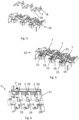
- the Fig. 1 to 5 show a switching device 1 for arrangement on busbars 3 of a busbar system, wherein the switching device 1 in this case has a number of receiving areas 6 corresponding to the number of busbars 3 for the front-side reception of cylindrical fuses (not shown in detail), in this case D0 fuses, wherein the receiving areas 6 are arranged in a row along a longitudinal direction X of the switching device 1.
- An input current conductor 7 and an outgoing current conductor 8 are assigned to the respective receiving area 6.
- the switching device 1 has a front side 4, which is to be turned away from the busbars 3, and a rear side 5, which is to be turned towards the busbars 3.
- the switching device 1 has two oppositely formed, parallel side walls 11, 12, wherein the second side wall 12 is essentially flat, whereas the first side wall 11 has three recesses 18.
- the switching device 1 has a housing with two housing parts 9, 10, wherein the housing part 9 has the first side wall 11 and the housing part 10 has the second side wall 12.
- the two side walls 11, 12 extend substantially in the longitudinal direction X and in the vertical direction Z and perpendicular to a transverse direction Y of the switching device 1.
- the switching device 1 further has a front cover 13 pivotably mounted in the housing 9, 10 for covering the front of the three receiving areas 6.
- the switching device 1 has a manually operable actuating lever 14, which actuating lever 14 serves to switch the switching device 1.
- the actuating lever 14 interacts with a snap-action switching mechanism (not shown in detail), which in turn is connected to a slide mounted in the housing 9, 10. 31, which serves to switch switching contacts of the switching device 1.
- bridge contacts 15 are mounted in the slide, wherein these bridge contacts 15 are spaced apart from busbar contacts 16, which serve to contact the busbars 3, in a switched-off state of the switching device 1.
- the bridge contacts 15 are spaced apart from the respective input current conductor 7 in the switched-off position. This state is in the Fig. 5 shown.
- the slide 31 is displaced such that the respective bridge contact 15 contacts both the busbar contact 16 and the input current conductor 7.
- the device has, in addition to the switching device 1, three separate electronic components 2, wherein the three electronic components 2 are mounted in a locking manner in the respective recess 18 of the side wall 11.
- the electronic component 2 comprises a measuring board 17, to which a display means 28 in the form of a light-emitting diode and two contacting elements 21 in the form of spring contacts are attached. As shown in particular in the Fig. 8 As can be seen, the contacting elements 21 pass through openings 20 in the side wall 11 of the switching device 1 and contact the input current conductor 7 and the output current conductor 8 of the respective receiving area 6. In the Fig. 6 and 7 In the embodiment of the device shown, the electronic component 2 is a fuse monitor, with the indicator 28 lighting up when the electrical fuse is triggered. To enable the light-emitting diode 28 to be visible from the front 4 of the switching device 1, both the housing part 9 and the front cover 4 have recesses 29 in the area of the indicator 28.
- the respective electronic component 2 is arranged completely within the recess 18, so that an extension of the device in the transverse direction Y is not increased compared to an extension of the switching device 1 in the transverse direction Y.
- the electronic components 2 can be plugged onto the side wall 11 from the outside in the direction of the arrow 32, thus in the transverse direction Y.
- the side wall 11 has elastically deformable locking means 19 formed in the region of the recesses 18, wherein these locking means 19 engage behind the electronic component 2, namely the circuit board 17, on a side of the circuit board 17 facing away from the switching device 1.
- the electronic components 2 can be connected to the switching device 1 without tools.
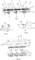
- the Fig. 10 to 16 show a second embodiment of the device, wherein the switching device 1 in this embodiment is identical to the switching device 1 in the first embodiment. Accordingly, different electronic components 2 can be connected to one and the same switching device 1.
- the electronic component 2 in addition to fuse monitoring, also enables measurement of the current flowing through the respective input current conductor 7.
- the electronic component 2 has a circuit board 17 extending over all three receiving areas 6, wherein this circuit board 17 is equipped with two contact elements 21 and a Hall sensor 23 for each of the three receiving areas 6.
- the contact elements 21, in turn, serve to contact the respective input current conductor 7 and the respective outgoing current conductor 8 for the purpose of fuse monitoring.
- the Hall sensor 23 serves to measure the current flowing through the input current conductor 7, wherein the respective Hall sensor 23 is additionally shielded by a shield plate 22 to shield against interference fields.
- the input current conductor 7 has a plate-shaped section 24 which protrudes in the direction of the side wall 11 relative to the other sections of the input current conductor 7.
- the plate-shaped section 24 is designed such that a main extension surface of the plate-shaped section 24 faces the side wall 11, in this case the plate-shaped section 24 or its main extension surface runs parallel to the side wall 11.
- the protruding, plate-shaped section 24 borders the side wall 11 in the region of the recess 18, with the Hall sensor 23 also bordering the recess 18 in the transverse direction Y, whereby the Hall sensor 23 is arranged particularly close to the plate-shaped section 24. This has a particularly favorable effect on the accuracy of the current measurement.
- the Fig. 9 shows the input current conductor 7 in a perspective view.
- a sheet metal development of the input current conductor 7 is essentially S-shaped.
- the electronic component 2 further comprises a communication interface 26 attached to the circuit board 17.
- the electronic component 2 has a separate electronics housing 27, wherein the electronics housing 27 is mounted in a locking manner in the side wall 11 of the housing 9, 10.
- the electronics housing 27 has a plurality of locking means 19 that engage with corresponding counterstructures of the housing part 9.
- the electronics housing 27 protrudes in the transverse direction Y relative to the side wall 11 and is flush with the housing 9, 10 in the vertical direction Z and in the longitudinal direction X.
- the electronics housing 27 has a plurality of ventilation openings and recesses 29, wherein the recesses 29 serve to ensure that display means 28, namely light-emitting diodes, connected to the circuit board 17 are visible from the front side 4 of the device.
- the electronic component 2 further comprises a light barrier 25 connected to the circuit board 17, wherein this light barrier 25 serves to detect the switching position of the slide 31.
- a shielding structure (not shown in detail) can be led out of the side wall 11 of the housing 9, 10, wherein this shielding structure is connected to the slide 31.
- this shielding structure or at least a section of this shielding structure is located in the area of the light barrier 25 or outside the light barrier 25, whereby a switching position of the slide 31 can be detected by means of the light barrier.
- the circuit board 17 and the electronics housing 27 can be plugged onto the side wall 11 from the outside in the direction of arrow 30, thus in the transverse direction Y. It is quite conceivable that the circuit board 17 is first connected to the housing 9, 10 of the switching device 1 and then the electronics housing 27 is connected to the housing 9, 10 of the switching device 1.
- the Figures 17 and 18 show a third embodiment of the invention, which differs from the second embodiment essentially in the design and configuration of the circuit board 17.
- the third embodiment does not have Hall sensors for current measurement. Accordingly, shielding plates can be omitted in the third embodiment.
- the third embodiment serves for fuse monitoring, whereby the status of the respective fuse can be transmitted to external evaluation, monitoring, and/or control devices via the communication interface 26.
Landscapes
- Engineering & Computer Science (AREA)
- Power Engineering (AREA)
- Switch Cases, Indication, And Locking (AREA)
Claims (15)
- Dispositif destiné à être disposé sur des barres omnibus (3), présentant un appareil de commutation (1), en particulier une barre de fusibles ou une barre de commutation de charge pour fusibles, et présentant un composant électronique (2), l'appareil de commutation (1) présentant un côté frontal (4) qui doit être tourné vers les barres omnibus (3) et présentant des zones de réception (6) pour fusibles agencées dans une direction longitudinale (X) de l'appareil de commutation (1), un conducteur (7) de courant d'entrée et un conducteur (8) de courant de sortie étant associés à chaque zone de réception (6), le conducteur (7) de courant d'entrée et le conducteur (8) de courant de sortie étant en connexion électrique l'un avec l'autre lorsqu'un fusible est disposé dans la zone de réception, le fusible interrompant la connexion électrique entre le conducteur (7) de courant d'entrée et le conducteur (8) de courant de sortie en cas d'apparition d'une surintensité, et l'appareil de commutation (1) présentant un boîtier (9, 10) avec une paroi latérale (11) s'étendant dans la direction longitudinale (X), le composant électronique (2) étant logé dans la paroi latérale (11), le composant électronique (2) étant relié de manière amovible à la paroi latérale (11) dans la zone d'un côté extérieur de la paroi latérale (11), le composant électronique (2) présentant un dispositif de mesure d'un courant traversant le conducteur (7) de courant d'entrée et/ou le conducteur (8) de courant de sortie et/ou d'une tension appliquée au conducteur (7) de courant d'entrée et/ou au conducteur (8) de courant de sortie et/ou présentant une prise de tension pour prélever une tension appliquée au conducteur (7) de courant d'entrée et/ou au conducteur (8) de courant de sortie, caractérisé en ce qu'au moins un des conducteurs (7) de courant d'entrée et/ou au moins un des conducteurs (8) de courant de sortie présente, par rapport aux autres parties du conducteur (7) de courant d'entrée ou du conducteur (8) de courant de sortie, une partie (24) en saillie en direction de la paroi latérale (11) du boîtier (9, 10), ledit au moins un conducteur (7) de courant d'entrée et/ou ledit au moins un conducteur (8) de courant de sortie présentant une partie intermédiaire en forme de U avec deux branches et une barrette reliant ces deux branches entre elles, les branches étant opposées à la paroi latérale (11) du boîtier (9, 10), la barrette formant la partie en saillie (24).
- Dispositif selon la revendication 1, dans lequel ledit au moins un conducteur (7) de courant d'entrée et/ou ledit au moins un conducteur (8) de courant de sortie comprend une partie (24) en forme de plaque, la partie (24) en forme de plaque étant conçue de telle sorte qu'une surface d'extension principale de la partie (24) en forme de plaque est tournée vers la paroi latérale (11) du boîtier (9, 10), la partie (24) en forme de plaque formant la partie en saillie (24).
- Dispositif selon l'une des revendications 1 à 2, dans lequel la paroi latérale (11) du boîtier (9, 10) présente, sur une face extérieure de la paroi latérale (11), une structure de support pour supporter le composant électronique (2), le composant électronique (2) étant maintenu par serrage et/ou par encliquetage dans la paroi latérale (11).
- Dispositif selon l'une des revendications 1 à 3, dans lequel la paroi latérale (11) du boîtier (9, 10) présente un évidement (18), l'évidement (18) recevant le composant électronique (2).
- Dispositif selon la revendication 4, dans lequel la paroi latérale (11) présente un nombre d'évidements (18) correspondant au nombre de zones de réception, l'évidement (18) respectif recevant un composant électronique (2).
- Dispositif selon la revendication 4 ou la revendication 5, dans lequel la partie en forme de plaque (24) et/ou la partie en saillie (24) est adjacente à la paroi latérale (11) du boîtier (9, 10) dans la zone de l'évidement (18).
- Dispositif selon l'une des revendications 1 à 6, dans lequel le composant électronique (2) présente une platine (17), la platine (17) coopérant mécaniquement avec la paroi latérale (11) du boîtier (9, 10) pour le montage du composant électronique (2) dans la paroi latérale (11).
- Dispositif selon l'une des revendications 1 à 7, dans lequel le composant électronique (2) présente au moins un élément de contact (21), chaque élément de contact (21) traversant la paroi latérale (11) du boîtier (9, 10).
- Dispositif selon la revendication 8, dans lequel l'élément de contact (21) respectif est en contact avec l'un des conducteurs (7) de courant d'entrée et/ou l'un des conducteurs (8) de courant de sortie.
- Dispositif selon l'une des revendications 1 à 9, dans lequel le composant électronique (2) présente un boîtier électronique (27), le boîtier électronique (27) étant logé dans la paroi latérale (11) du boîtier (9, 10) .
- Dispositif selon la revendication 10, dans lequel le boîtier électronique (27) fait saillie dans la direction transversale (Y) par rapport à la paroi latérale (11) du boîtier (9, 10).
- Dispositif selon la revendication 10 ou la revendication 11, dans lequel le composant électronique (2) présente une carte électronique (17), le boîtier électronique (27) recevant la carte électronique (17).
- Dispositif selon l'une des revendications 1 à 12, dans lequel la paroi latérale (11) du boîtier (9, 10) de l'appareil de commutation (1) est conçue pour être protégée contre les contacts avec les doigts, en particulier le boîtier électronique (27) et/ou la platine (17) logée dans la paroi latérale est protégée contre les contacts avec les doigts lorsqu'elle est logée dans l'appareil de commutation (1).
- Dispositif selon l'une des revendications 1 à 13, dans lequel le composant électronique (2) présente un dispositif de contrôle de fusibles.
- Dispositif selon l'une des revendications 1 à 14, dans lequel le composant électronique (2) présente un moyen d'affichage (28), le moyen d'affichage (28) étant visible depuis la face avant (4).
Priority Applications (2)
| Application Number | Priority Date | Filing Date | Title |
|---|---|---|---|
| EP21166330.7A EP4068329B1 (fr) | 2021-03-31 | 2021-03-31 | Dispositif destiné à l'agencement sur barres de distribution comprenant un appareil de commutation et un composant électronique |
| PL21166330.7T PL4068329T3 (pl) | 2021-03-31 | 2021-03-31 | Urządzenie do rozmieszczania na szynach zbiorczych zawierające przełącznik i element elektroniczny |
Applications Claiming Priority (1)
| Application Number | Priority Date | Filing Date | Title |
|---|---|---|---|
| EP21166330.7A EP4068329B1 (fr) | 2021-03-31 | 2021-03-31 | Dispositif destiné à l'agencement sur barres de distribution comprenant un appareil de commutation et un composant électronique |
Publications (2)
| Publication Number | Publication Date |
|---|---|
| EP4068329A1 EP4068329A1 (fr) | 2022-10-05 |
| EP4068329B1 true EP4068329B1 (fr) | 2025-03-19 |
Family
ID=75362341
Family Applications (1)
| Application Number | Title | Priority Date | Filing Date |
|---|---|---|---|
| EP21166330.7A Active EP4068329B1 (fr) | 2021-03-31 | 2021-03-31 | Dispositif destiné à l'agencement sur barres de distribution comprenant un appareil de commutation et un composant électronique |
Country Status (2)
| Country | Link |
|---|---|
| EP (1) | EP4068329B1 (fr) |
| PL (1) | PL4068329T3 (fr) |
Families Citing this family (1)
| Publication number | Priority date | Publication date | Assignee | Title |
|---|---|---|---|---|
| DE102024105906B3 (de) | 2024-03-01 | 2025-06-05 | Klaus Bruchmann Gmbh | Modulares sicherungslasttrennschalter-system sowie messmodul für ein solches system |
Family Cites Families (5)
| Publication number | Priority date | Publication date | Assignee | Title |
|---|---|---|---|---|
| DE29705224U1 (de) | 1997-03-22 | 1997-06-26 | Jean Müller GmbH Elektrotechnische Fabrik, 65343 Eltville | Einrichtung mit einer NH-Sicherungs- oder NH-Lastschaltleiste sowie einem Wandler |
| AT409675B (de) * | 1999-06-04 | 2002-10-25 | Schneider Schaltgeraetebau Und | Überwachungssystem für nh-sicherungssysteme |
| DE10129176C1 (de) * | 2001-06-19 | 2002-10-17 | Mueller Jean Ohg Elektrotech | Mehrpoliges Schaltgerät für den Einsatz auf Sammelschienensystemen |
| DE102017011374A1 (de) * | 2017-12-11 | 2019-06-13 | Fachhochschule Südwestfalen | Schutzeinrichtung für Niederspannungsanlagen mit integrierter Messelektronik |
| EP3671785A1 (fr) * | 2018-12-19 | 2020-06-24 | Jean Müller GmbH Elektrotechnische Fabrik | Agencement d'une partie porteuse et d'une partie supérieure d'un dispositif de commutation doté des composants d'une électronique intégrés dans l'agencement |
-
2021
- 2021-03-31 EP EP21166330.7A patent/EP4068329B1/fr active Active
- 2021-03-31 PL PL21166330.7T patent/PL4068329T3/pl unknown
Also Published As
| Publication number | Publication date |
|---|---|
| EP4068329A1 (fr) | 2022-10-05 |
| PL4068329T3 (pl) | 2025-07-14 |
Similar Documents
| Publication | Publication Date | Title |
|---|---|---|
| EP3447785B1 (fr) | Distributeur de courant | |
| EP2546856B1 (fr) | Baguette pour fusibles NH | |
| EP0170161B1 (fr) | Appareil d'installation pour systèmes de barres omnibus | |
| EP2587513A1 (fr) | Commutateur d'installation doté d'une unité de capteur de courant | |
| DE102007027522B3 (de) | Schaltgerät | |
| DE202019100399U1 (de) | Lasttrennschaltervorrichtung und Schaltersicherungsvorrichtung mit Sicherung | |
| EP3671785A1 (fr) | Agencement d'une partie porteuse et d'une partie supérieure d'un dispositif de commutation doté des composants d'une électronique intégrés dans l'agencement | |
| DE102017011374A1 (de) | Schutzeinrichtung für Niederspannungsanlagen mit integrierter Messelektronik | |
| EP1120873B1 (fr) | Dispositif de support pour le montage d'au moins un appareil électrique sur un rail DIN | |
| EP4068329A1 (fr) | Dispositif destiné à l'agencement sur barres de distribution comprenant un appareil de commutation et un composant électronique | |
| DE202019001746U1 (de) | Kompakt-Schutzschaltgerät | |
| DE102020118110A1 (de) | Überspannungsschutzanordnung | |
| DE10344735B4 (de) | Elektrisches Installationsgerät | |
| DE102017011373A1 (de) | Mess- und Steuerelektronik für Niederspannungsschaltanlagen | |
| DE102005049873B4 (de) | Überspannungsableiter-Anordnung mit einer als Bestandteil eines Gehäuses ausführbaren Trägerplatte | |
| DE102020209257A1 (de) | Befestigungsvorrichtung und Reiheneinbaugerät | |
| DE19950995A1 (de) | Installationsschalter | |
| EP2983191B1 (fr) | Système de détection d'arcs électriques parasites dans un réseau basse tension | |
| DE102023202388A1 (de) | Geräte-Modul, Reiheneinbaugerät und Kontaktfeder | |
| DE102019118951B4 (de) | Überspannungsschutzanordnung | |
| DE102022202311A1 (de) | Elektronisch schaltendes Reiheneinbaugerät und Isolierstoffgehäuse | |
| EP2482081B1 (fr) | Dispositif de raccordement pour un compteur d'électricité | |
| DE10216371A1 (de) | Hilfsschalter | |
| DE10146502A1 (de) | Elektrische Installationsverteilung | |
| DE102007048412A1 (de) | Schutzschalteinrichtung und Schutzschaltgerät |
Legal Events
| Date | Code | Title | Description |
|---|---|---|---|
| PUAI | Public reference made under article 153(3) epc to a published international application that has entered the european phase |
Free format text: ORIGINAL CODE: 0009012 |
|
| STAA | Information on the status of an ep patent application or granted ep patent |
Free format text: STATUS: THE APPLICATION HAS BEEN PUBLISHED |
|
| AK | Designated contracting states |
Kind code of ref document: A1 Designated state(s): AL AT BE BG CH CY CZ DE DK EE ES FI FR GB GR HR HU IE IS IT LI LT LU LV MC MK MT NL NO PL PT RO RS SE SI SK SM TR |
|
| STAA | Information on the status of an ep patent application or granted ep patent |
Free format text: STATUS: REQUEST FOR EXAMINATION WAS MADE |
|
| 17P | Request for examination filed |
Effective date: 20230322 |
|
| RBV | Designated contracting states (corrected) |
Designated state(s): AL AT BE BG CH CY CZ DE DK EE ES FI FR GB GR HR HU IE IS IT LI LT LU LV MC MK MT NL NO PL PT RO RS SE SI SK SM TR |
|
| P01 | Opt-out of the competence of the unified patent court (upc) registered |
Effective date: 20230519 |
|
| GRAP | Despatch of communication of intention to grant a patent |
Free format text: ORIGINAL CODE: EPIDOSNIGR1 |
|
| STAA | Information on the status of an ep patent application or granted ep patent |
Free format text: STATUS: GRANT OF PATENT IS INTENDED |
|
| RIC1 | Information provided on ipc code assigned before grant |
Ipc: H01H 85/30 20060101ALN20241108BHEP Ipc: H01H 31/12 20060101ALN20241108BHEP Ipc: H01H 9/10 20060101ALN20241108BHEP Ipc: H01H 9/02 20060101ALI20241108BHEP Ipc: H01H 85/02 20060101AFI20241108BHEP |
|
| INTG | Intention to grant announced |
Effective date: 20241125 |
|
| GRAS | Grant fee paid |
Free format text: ORIGINAL CODE: EPIDOSNIGR3 |
|
| GRAA | (expected) grant |
Free format text: ORIGINAL CODE: 0009210 |
|
| STAA | Information on the status of an ep patent application or granted ep patent |
Free format text: STATUS: THE PATENT HAS BEEN GRANTED |
|
| AK | Designated contracting states |
Kind code of ref document: B1 Designated state(s): AL AT BE BG CH CY CZ DE DK EE ES FI FR GB GR HR HU IE IS IT LI LT LU LV MC MK MT NL NO PL PT RO RS SE SI SK SM TR |
|
| REG | Reference to a national code |
Ref country code: GB Ref legal event code: FG4D Free format text: NOT ENGLISH |
|
| REG | Reference to a national code |
Ref country code: CH Ref legal event code: EP |
|
| REG | Reference to a national code |
Ref country code: DE Ref legal event code: R096 Ref document number: 502021006951 Country of ref document: DE |
|
| REG | Reference to a national code |
Ref country code: IE Ref legal event code: FG4D Free format text: LANGUAGE OF EP DOCUMENT: GERMAN |
|
| PG25 | Lapsed in a contracting state [announced via postgrant information from national office to epo] |
Ref country code: RS Free format text: LAPSE BECAUSE OF FAILURE TO SUBMIT A TRANSLATION OF THE DESCRIPTION OR TO PAY THE FEE WITHIN THE PRESCRIBED TIME-LIMIT Effective date: 20250619 |
|
| PG25 | Lapsed in a contracting state [announced via postgrant information from national office to epo] |
Ref country code: FI Free format text: LAPSE BECAUSE OF FAILURE TO SUBMIT A TRANSLATION OF THE DESCRIPTION OR TO PAY THE FEE WITHIN THE PRESCRIBED TIME-LIMIT Effective date: 20250319 |
|
| REG | Reference to a national code |
Ref country code: LT Ref legal event code: MG9D |
|
| PG25 | Lapsed in a contracting state [announced via postgrant information from national office to epo] |
Ref country code: NO Free format text: LAPSE BECAUSE OF FAILURE TO SUBMIT A TRANSLATION OF THE DESCRIPTION OR TO PAY THE FEE WITHIN THE PRESCRIBED TIME-LIMIT Effective date: 20250619 |
|
| PG25 | Lapsed in a contracting state [announced via postgrant information from national office to epo] |
Ref country code: HR Free format text: LAPSE BECAUSE OF FAILURE TO SUBMIT A TRANSLATION OF THE DESCRIPTION OR TO PAY THE FEE WITHIN THE PRESCRIBED TIME-LIMIT Effective date: 20250319 |
|
| PG25 | Lapsed in a contracting state [announced via postgrant information from national office to epo] |
Ref country code: LV Free format text: LAPSE BECAUSE OF FAILURE TO SUBMIT A TRANSLATION OF THE DESCRIPTION OR TO PAY THE FEE WITHIN THE PRESCRIBED TIME-LIMIT Effective date: 20250319 |
|
| PG25 | Lapsed in a contracting state [announced via postgrant information from national office to epo] |
Ref country code: GR Free format text: LAPSE BECAUSE OF FAILURE TO SUBMIT A TRANSLATION OF THE DESCRIPTION OR TO PAY THE FEE WITHIN THE PRESCRIBED TIME-LIMIT Effective date: 20250620 Ref country code: BG Free format text: LAPSE BECAUSE OF FAILURE TO SUBMIT A TRANSLATION OF THE DESCRIPTION OR TO PAY THE FEE WITHIN THE PRESCRIBED TIME-LIMIT Effective date: 20250319 |
|
| REG | Reference to a national code |
Ref country code: NL Ref legal event code: MP Effective date: 20250319 |
|
| PG25 | Lapsed in a contracting state [announced via postgrant information from national office to epo] |
Ref country code: NL Free format text: LAPSE BECAUSE OF FAILURE TO SUBMIT A TRANSLATION OF THE DESCRIPTION OR TO PAY THE FEE WITHIN THE PRESCRIBED TIME-LIMIT Effective date: 20250319 |
|
| PG25 | Lapsed in a contracting state [announced via postgrant information from national office to epo] |
Ref country code: SE Free format text: LAPSE BECAUSE OF FAILURE TO SUBMIT A TRANSLATION OF THE DESCRIPTION OR TO PAY THE FEE WITHIN THE PRESCRIBED TIME-LIMIT Effective date: 20250319 |
|
| PG25 | Lapsed in a contracting state [announced via postgrant information from national office to epo] |
Ref country code: SM Free format text: LAPSE BECAUSE OF FAILURE TO SUBMIT A TRANSLATION OF THE DESCRIPTION OR TO PAY THE FEE WITHIN THE PRESCRIBED TIME-LIMIT Effective date: 20250319 |
|
| PG25 | Lapsed in a contracting state [announced via postgrant information from national office to epo] |
Ref country code: ES Free format text: LAPSE BECAUSE OF FAILURE TO SUBMIT A TRANSLATION OF THE DESCRIPTION OR TO PAY THE FEE WITHIN THE PRESCRIBED TIME-LIMIT Effective date: 20250319 Ref country code: PT Free format text: LAPSE BECAUSE OF FAILURE TO SUBMIT A TRANSLATION OF THE DESCRIPTION OR TO PAY THE FEE WITHIN THE PRESCRIBED TIME-LIMIT Effective date: 20250721 |
|
| PG25 | Lapsed in a contracting state [announced via postgrant information from national office to epo] |
Ref country code: IT Free format text: LAPSE BECAUSE OF FAILURE TO SUBMIT A TRANSLATION OF THE DESCRIPTION OR TO PAY THE FEE WITHIN THE PRESCRIBED TIME-LIMIT Effective date: 20250319 |
|
| PG25 | Lapsed in a contracting state [announced via postgrant information from national office to epo] |
Ref country code: CZ Free format text: LAPSE BECAUSE OF FAILURE TO SUBMIT A TRANSLATION OF THE DESCRIPTION OR TO PAY THE FEE WITHIN THE PRESCRIBED TIME-LIMIT Effective date: 20250319 Ref country code: EE Free format text: LAPSE BECAUSE OF FAILURE TO SUBMIT A TRANSLATION OF THE DESCRIPTION OR TO PAY THE FEE WITHIN THE PRESCRIBED TIME-LIMIT Effective date: 20250319 |
|
| PG25 | Lapsed in a contracting state [announced via postgrant information from national office to epo] |
Ref country code: RO Free format text: LAPSE BECAUSE OF FAILURE TO SUBMIT A TRANSLATION OF THE DESCRIPTION OR TO PAY THE FEE WITHIN THE PRESCRIBED TIME-LIMIT Effective date: 20250319 |
|
| REG | Reference to a national code |
Ref country code: CH Ref legal event code: H13 Free format text: ST27 STATUS EVENT CODE: U-0-0-H10-H13 (AS PROVIDED BY THE NATIONAL OFFICE) Effective date: 20251024 |
|
| PG25 | Lapsed in a contracting state [announced via postgrant information from national office to epo] |
Ref country code: SK Free format text: LAPSE BECAUSE OF FAILURE TO SUBMIT A TRANSLATION OF THE DESCRIPTION OR TO PAY THE FEE WITHIN THE PRESCRIBED TIME-LIMIT Effective date: 20250319 |
|
| PG25 | Lapsed in a contracting state [announced via postgrant information from national office to epo] |
Ref country code: IS Free format text: LAPSE BECAUSE OF FAILURE TO SUBMIT A TRANSLATION OF THE DESCRIPTION OR TO PAY THE FEE WITHIN THE PRESCRIBED TIME-LIMIT Effective date: 20250719 |
|
| PG25 | Lapsed in a contracting state [announced via postgrant information from national office to epo] |
Ref country code: LU Free format text: LAPSE BECAUSE OF NON-PAYMENT OF DUE FEES Effective date: 20250331 |
|
| REG | Reference to a national code |
Ref country code: BE Ref legal event code: MM Effective date: 20250331 |
|
| PG25 | Lapsed in a contracting state [announced via postgrant information from national office to epo] |
Ref country code: MC Free format text: LAPSE BECAUSE OF FAILURE TO SUBMIT A TRANSLATION OF THE DESCRIPTION OR TO PAY THE FEE WITHIN THE PRESCRIBED TIME-LIMIT Effective date: 20250319 |
|
| REG | Reference to a national code |
Ref country code: DE Ref legal event code: R097 Ref document number: 502021006951 Country of ref document: DE |
|
| PG25 | Lapsed in a contracting state [announced via postgrant information from national office to epo] |
Ref country code: DK Free format text: LAPSE BECAUSE OF FAILURE TO SUBMIT A TRANSLATION OF THE DESCRIPTION OR TO PAY THE FEE WITHIN THE PRESCRIBED TIME-LIMIT Effective date: 20250319 |
|
| PG25 | Lapsed in a contracting state [announced via postgrant information from national office to epo] |
Ref country code: BE Free format text: LAPSE BECAUSE OF NON-PAYMENT OF DUE FEES Effective date: 20250331 |
|
| PG25 | Lapsed in a contracting state [announced via postgrant information from national office to epo] |
Ref country code: CH Free format text: LAPSE BECAUSE OF NON-PAYMENT OF DUE FEES Effective date: 20250331 |
|
| PG25 | Lapsed in a contracting state [announced via postgrant information from national office to epo] |
Ref country code: IE Free format text: LAPSE BECAUSE OF NON-PAYMENT OF DUE FEES Effective date: 20250331 |
|
| PLBE | No opposition filed within time limit |
Free format text: ORIGINAL CODE: 0009261 |
|
| STAA | Information on the status of an ep patent application or granted ep patent |
Free format text: STATUS: NO OPPOSITION FILED WITHIN TIME LIMIT |
|
| REG | Reference to a national code |
Ref country code: CH Ref legal event code: L10 Free format text: ST27 STATUS EVENT CODE: U-0-0-L10-L00 (AS PROVIDED BY THE NATIONAL OFFICE) Effective date: 20260128 |
|
| 26N | No opposition filed |
Effective date: 20251222 |
|
| GBPC | Gb: european patent ceased through non-payment of renewal fee |
Effective date: 20250619 |
|
| PG25 | Lapsed in a contracting state [announced via postgrant information from national office to epo] |
Ref country code: GB Free format text: LAPSE BECAUSE OF NON-PAYMENT OF DUE FEES Effective date: 20250619 |
|
| PGFP | Annual fee paid to national office [announced via postgrant information from national office to epo] |
Ref country code: DE Payment date: 20260326 Year of fee payment: 6 |
|
| PGFP | Annual fee paid to national office [announced via postgrant information from national office to epo] |
Ref country code: AT Payment date: 20260320 Year of fee payment: 6 |
|
| PG25 | Lapsed in a contracting state [announced via postgrant information from national office to epo] |
Ref country code: FR Free format text: LAPSE BECAUSE OF NON-PAYMENT OF DUE FEES Effective date: 20250519 |
|
| PGFP | Annual fee paid to national office [announced via postgrant information from national office to epo] |
Ref country code: PL Payment date: 20260323 Year of fee payment: 6 |