EP4068362B1 - Dispositif de capture d'image et procédé de commande - Google Patents
Dispositif de capture d'image et procédé de commande Download PDFInfo
- Publication number
- EP4068362B1 EP4068362B1 EP20894775.4A EP20894775A EP4068362B1 EP 4068362 B1 EP4068362 B1 EP 4068362B1 EP 20894775 A EP20894775 A EP 20894775A EP 4068362 B1 EP4068362 B1 EP 4068362B1
- Authority
- EP
- European Patent Office
- Prior art keywords
- pixels
- reset
- signal
- row
- imaging device
- Prior art date
- Legal status (The legal status is an assumption and is not a legal conclusion. Google has not performed a legal analysis and makes no representation as to the accuracy of the status listed.)
- Active
Links
Images






Classifications
-
- H—ELECTRICITY
- H04—ELECTRIC COMMUNICATION TECHNIQUE
- H04N—PICTORIAL COMMUNICATION, e.g. TELEVISION
- H04N25/00—Circuitry of solid-state image sensors [SSIS]; Control thereof
- H04N25/60—Noise processing, e.g. detecting, correcting, reducing or removing noise
- H04N25/616—Noise processing, e.g. detecting, correcting, reducing or removing noise involving a correlated sampling function, e.g. correlated double sampling [CDS] or triple sampling
-
- H—ELECTRICITY
- H04—ELECTRIC COMMUNICATION TECHNIQUE
- H04N—PICTORIAL COMMUNICATION, e.g. TELEVISION
- H04N25/00—Circuitry of solid-state image sensors [SSIS]; Control thereof
- H04N25/40—Extracting pixel data from image sensors by controlling scanning circuits, e.g. by modifying the number of pixels sampled or to be sampled
-
- H—ELECTRICITY
- H04—ELECTRIC COMMUNICATION TECHNIQUE
- H04N—PICTORIAL COMMUNICATION, e.g. TELEVISION
- H04N25/00—Circuitry of solid-state image sensors [SSIS]; Control thereof
- H04N25/50—Control of the SSIS exposure
-
- H—ELECTRICITY
- H04—ELECTRIC COMMUNICATION TECHNIQUE
- H04N—PICTORIAL COMMUNICATION, e.g. TELEVISION
- H04N25/00—Circuitry of solid-state image sensors [SSIS]; Control thereof
- H04N25/50—Control of the SSIS exposure
- H04N25/53—Control of the integration time
- H04N25/532—Control of the integration time by controlling global shutters in CMOS SSIS
-
- H—ELECTRICITY
- H04—ELECTRIC COMMUNICATION TECHNIQUE
- H04N—PICTORIAL COMMUNICATION, e.g. TELEVISION
- H04N25/00—Circuitry of solid-state image sensors [SSIS]; Control thereof
- H04N25/60—Noise processing, e.g. detecting, correcting, reducing or removing noise
- H04N25/63—Noise processing, e.g. detecting, correcting, reducing or removing noise applied to dark current
-
- H—ELECTRICITY
- H04—ELECTRIC COMMUNICATION TECHNIQUE
- H04N—PICTORIAL COMMUNICATION, e.g. TELEVISION
- H04N25/00—Circuitry of solid-state image sensors [SSIS]; Control thereof
- H04N25/60—Noise processing, e.g. detecting, correcting, reducing or removing noise
- H04N25/65—Noise processing, e.g. detecting, correcting, reducing or removing noise applied to reset noise, e.g. KTC noise related to CMOS structures by techniques other than CDS
-
- H—ELECTRICITY
- H04—ELECTRIC COMMUNICATION TECHNIQUE
- H04N—PICTORIAL COMMUNICATION, e.g. TELEVISION
- H04N25/00—Circuitry of solid-state image sensors [SSIS]; Control thereof
- H04N25/70—SSIS architectures; Circuits associated therewith
- H04N25/76—Addressed sensors, e.g. MOS or CMOS sensors
-
- H—ELECTRICITY
- H04—ELECTRIC COMMUNICATION TECHNIQUE
- H04N—PICTORIAL COMMUNICATION, e.g. TELEVISION
- H04N25/00—Circuitry of solid-state image sensors [SSIS]; Control thereof
- H04N25/70—SSIS architectures; Circuits associated therewith
- H04N25/76—Addressed sensors, e.g. MOS or CMOS sensors
- H04N25/77—Pixel circuitry, e.g. memories, A/D converters, pixel amplifiers, shared circuits or shared components
-
- H—ELECTRICITY
- H04—ELECTRIC COMMUNICATION TECHNIQUE
- H04N—PICTORIAL COMMUNICATION, e.g. TELEVISION
- H04N25/00—Circuitry of solid-state image sensors [SSIS]; Control thereof
- H04N25/70—SSIS architectures; Circuits associated therewith
- H04N25/76—Addressed sensors, e.g. MOS or CMOS sensors
- H04N25/7795—Circuitry for generating timing or clock signals
-
- H—ELECTRICITY
- H10—SEMICONDUCTOR DEVICES; ELECTRIC SOLID-STATE DEVICES NOT OTHERWISE PROVIDED FOR
- H10F—INORGANIC SEMICONDUCTOR DEVICES SENSITIVE TO INFRARED RADIATION, LIGHT, ELECTROMAGNETIC RADIATION OF SHORTER WAVELENGTH OR CORPUSCULAR RADIATION
- H10F39/00—Integrated devices, or assemblies of multiple devices, comprising at least one element covered by group H10F30/00, e.g. radiation detectors comprising photodiode arrays
- H10F39/10—Integrated devices
- H10F39/12—Image sensors
-
- H—ELECTRICITY
- H10—SEMICONDUCTOR DEVICES; ELECTRIC SOLID-STATE DEVICES NOT OTHERWISE PROVIDED FOR
- H10K—ORGANIC ELECTRIC SOLID-STATE DEVICES
- H10K39/00—Integrated devices, or assemblies of multiple devices, comprising at least one organic radiation-sensitive element covered by group H10K30/00
- H10K39/30—Devices controlled by radiation
- H10K39/32—Organic image sensors
Definitions
- the present disclosure relates to an imaging device and so on comprising a photoelectric converting portion that generates charge upon being illuminated with light.
- CMOS Complementary Metal Oxide Semiconductor
- CMOS solid-state imaging elements for example, a CDS (Correlated Double Sampling) technology disclosed in PTL 1 has been widely used.
- CDS Correlated Double Sampling
- the pixel circuit shown in Fig. 2 in PTL 1 is constituted by a PD (photodetector) portion for detecting an optical signal, an FD (floating diffusion) portion for converting charge generated by the PD portion into a voltage signal and temporarily holding the voltage signal, a TX transistor for transferring the charge signal from the PD portion to the FD portion, a RES transistor for resetting a voltage of the FD portion, an AMP transistor for amplifying the voltage signal of the FD portion, and a SEL transistor for outputting the amplified signal.
- the PD portion is constituted by a photodiode.
- the TX transistor is controlled with a control signal ⁇ TX
- the RES transistor is controlled with a control signal ⁇ RST
- the SEL transistor is controlled with a control signal ⁇ SEL.
- ⁇ RST is first set to a high level to turn on the RES transistor, so that charge accumulated in the FD portion is reset.
- ⁇ RST is set to a low level to turn off the RES transistor, and then ⁇ SEL is set to a high level to turn on the SEL transistor, so that a reset voltage is output.
- kTC noise reset noise
- time-series fluctuations occur.
- ⁇ TX is set to a high level to turn on the TX transistor, so that the signal charge accumulated in the FD portion is transferred to the PD portion.
- ⁇ TX is set to a low level to turn off the TX transistor, and the signal voltage is output. Since the signal voltage becomes a signal that has changed from the reset voltage by a voltage corresponding to the accumulated signal charge, a circuit at a subsequent stage determines a difference between the reset voltage (in other words, reset charge) and the signal voltage (in other words, the reset charge + the signal charge) to make it possible to cancel the kTC noise and to make it possible to detect only a voltage corresponding to the accumulated signal charge.
- reset charge the reset charge + the signal charge
- the above-described technology is the CDS technology and has an advantage of significantly reducing reset noise (kTC noise) that occurs during reset of the pixel section, and the reset noise reduction due to the CDS technology is also one factor for why the CMOS solid-state imaging elements are becoming mainly used.
- US 2010/271518 A1 and US 2006/077282 A1 disclose imaging devices which can reduce the shutter time lag.
- An object of the present disclosure is to provide an imaging device and so on that can reduce, in a state in which noise is reduced, the time lag from the trigger signal for giving an instruction for starting exposure until the start of the exposure.
- An imaging device according to one aspect of the present disclosure is defined in claim 1.
- a control method according to one aspect of the present disclosure is defined in claim 11.
- the imaging device can reduce, in a state in which noise is reduced, the time lag from the trigger signal for giving an instruction for starting the exposure until the start of the exposure.
- the CDS technology described above is based on the premise that signal charge generated in PD portions for detecting optical signals is completely transferred during transfer to FD portions where the signal charge is converted into voltage signals. In order to realize the complete transfer, there are problems that the processes become complicated, and the manufacturing cost increases, and so on.
- a solid-state imaging element having pixels with a structure for realizing a global shutter has been recently proposed as a solid-state imaging element for imaging a high-speed operating object without distortion, as disclosed in PTL 2.
- the solid-state imaging element disclosed in PTL 2 since charge in the PD portions in all pixels is transferred to the FD portions at a time, and then the charge is sequentially read out for each row, the CDS technology for reading out reset voltages before signal voltages in the FD portions are read out cannot be applied thereto. Accordingly, the FD portions are reset after the signal voltages in the FD portions are read out, and the reset voltages are read out, and differences between the signal voltages and the reset voltages are determined.
- reset noise included in the signal voltages and reset noise included the reset voltages are not correlated with each other, there are problems that the reset noise cannot be removed, and random noise increases compared with readout using the above-described CDS technology.
- an organic CMOS sensor in which an organic photoelectric conversion film is used in PD portions has been proposed, like that disclosed in PTL 3, as a solid-state imaging element for solving a sensitivity decline due to a decrease in the areas of the PD portions.
- this organic CMOS sensor when organic photoelectric conversion films, which are light receiving portions, are provided above readout circuits, the areas of the light receiving portions can be increased even when the pixel size is reduced. Thus, it is possible to realize high sensitivity.
- sensors using photoelectric conversion films like organic CMOS sensors, have a structure in which PD portions and semiconductor layers are electrically connected through metal wires, signal charge cannot be completely transferred. Accordingly, in general, a structure in which the signal charge in the PD portions is read out through electrical connection of the PD portions and the FD portions is employed so as to prevent occurrence of incomplete transfer noise and afterimage.
- CDS technology is a technology that is effective in reducing the reset noise, there are problems that it brings about a manufacturing cost increase involved with complication of the processes and cannot be further applied to CMOS solid-state imaging elements having a structure that has advantages in terms of functions and performance.
- the trigger signal is, for example, a signal issued according to an operation of another machine or the like, a signal issued when a shutter button or the like is pressed by a person, or the like.
- an object of the present disclosure is to provide an imaging device comprising a solid-state imaging element that appropriately removes reset noise and that can start exposure at high speed in response to an external trigger signal.
- An imaging device according to claim 1 is provided.
- the control circuit causes the pixels belonging to at least one row to execute the exposure operation without performing the reset operation.
- the time from the reception of the trigger signal to the exposure operation is reduced compared with a case in which the reset operation is executed on all the pixels after the trigger signal is received.
- the potentials are initialized before the signal charge is accumulated, and in particular, when the reset operation is performed in conjunction with reduction of reset noise, noise in the signal charge in the pixels belonging to at least one row is reduced.
- the imaging device makes it possible to reduce the time lag from the trigger signal for giving an instruction for starting the exposure until the start of the exposure, in a state in which noise is reduced.
- control circuit may cause all the plurality of pixels to sequentially perform the reset operation for each row or for two or more rows at a time.
- control circuit may cause the pixels included in the plurality of pixels and belonging to at least one row to perform the reset operation a plurality of times.
- the reset operation is performed on the pixels belonging to at least one row a plurality of times.
- the charge accumulated in the charge accumulation portions owing to dark current or the like is initialized again by the reset operation.
- the reset operation is repeatedly performed on the pixels until the control circuit receives the trigger signal.
- the charge accumulated in the charge accumulation portions owing to dark current or the like after the reset operation is performed is repeatedly initialized by the reset operation.
- the imaging device according to this aspect can further reduce noise.
- control circuit may cause the plurality of pixels to sequentially perform, for each row or for two or more rows at a time, the reset operation up to a row different from a row at which the reset operation was started, and may cause, after the exposure operation, the plurality of pixels to sequentially perform a readout operation for outputting signals corresponding to the signal charge accumulated in the charge accumulation portions, the readout operation being performed for each row or for two or more rows at a time from a next-order row of a row at which the reset operation was ended.
- each of the plurality of pixels may include a feedback circuit for negatively feeding back a potential of the charge accumulation portion in the reset operation.
- the imaging device can further reduce noise.
- each of the plurality of pixels may include a circuit for reducing reset noise that occurs in the reset operation.
- the imaging device can further reduce noise.
- the imaging device may further comprise a voltage supply circuit.
- the photoelectric converting portion may include a counter electrode electrically connected to the voltage supply circuit, pixel electrodes electrically connected to the charge accumulation portion, and a photoelectric conversion layer located between the counter electrode and the pixel electrodes.
- the control circuit may cause the voltage supply circuit to apply a voltage to the counter electrode to form an electric field in the photoelectric conversion layer to thereby cause the plurality of pixels to perform the exposure operation.
- the time lag from the trigger signal for giving an instruction for starting the exposure until the start of the exposure can be reduced in a state in which noise is reduced. Also, since the exposure operation is performed upon voltage application to the counter electrode, it is possible to suppress the circuit becoming complicated.
- control method according to one aspect of the present disclosure is defined in claim 11.
- the control method can reduce, in a state in which noise is reduced, the time lag from the trigger signal for giving an instruction for starting the exposure until the start of the exposure.
- the terms “above” and “below” do not refer to an upper direction (a vertically upper side) and a lower direction (a vertically lower side) in absolute spatial recognition and are used as terms defined by relative positional relationships based on the order of stacked layers in a stack configuration. Also, the terms “above” and “below” apply not only to cases in which two constituent elements are arranged with a gap therebetween and a constituent element exists between the two constituent elements and but also to cases in which two constituent elements are arranged to adhere to each other and the two constituent elements contact each other.
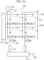
- Fig. 1A is a diagram schematically showing an exemplary circuit configuration of the imaging device 100 according to the present embodiment.
- the imaging device 100 is a stacked imaging element in one example and has a photoelectric conversion layer stacked on a semiconductor substrate.
- the imaging device 100 comprises a plurality of pixels 110 and peripheral circuitry.
- the peripheral circuitry includes a control circuit for controlling operations of the plurality of pixels 110. Upon receiving an external trigger signal, the control circuit causes the plurality of pixels 110 to perform an exposure operation.
- the pixels 110 are arrayed two-dimensionally to form a photosensitive region, which is a so-called pixel region.
- the pixels 110 may be arrayed one dimensionally.
- the imaging device 100 is a line sensor.
- the pixels 110 are arrayed in row directions and column directions.
- the row directions and the column directions refer to directions in which rows and columns extend, respectively. That is, vertical directions are the column directions, and horizontal directions are the row directions.
- Each of the pixels 110 is connected to a power-supply line 120.
- a predetermined power-supply voltage is supplied to each pixel 110 through the power-supply line 120.
- the imaging device 100 has an accumulation control line 130 through which the same constant voltage to all photoelectric conversion layers that photoelectrically convert incident light. However, when other control, such as fluctuation reduction, is performed, the constant voltage may be divided into some voltages for application.
- the peripheral circuitry includes a voltage supply circuit 140, a vertical scanning circuit 141, column signal processing circuits 142, a horizontal signal readout circuit 143, and constant-current sources 144.
- the vertical scanning circuit 141 is also referred to as a "row scanning circuit”
- the horizontal signal readout circuit 143 is also referred to as a "column scanning circuit”.
- the column signal processing circuits 142 and the constant-current sources 144 may be arranged for corresponding columns of the pixels 110 arrayed two-dimensionally.
- peripheral circuitry One example of a configuration of the peripheral circuitry will be described below.
- the voltage supply circuit 140 is connected to the accumulation control line 130. During operation of the imaging device 100, the voltage supply circuit 140 applies a predetermined bias voltage to a counter electrode 1b (details of which are described later) of the pixels 110 through the accumulation control line 130. A control circuit controls operations of the voltage supply circuit 140.
- the vertical scanning circuit 141 is connected to selection-control signal lines CON7 and amplification-control signal lines CON3.
- the amplification-control signal lines CON3 are referred to as “band-control signal lines”, and the selection-control signal lines CON7 are referred to as "address signal lines”.
- the vertical scanning circuit 141 is a portion of the control circuit that controls operations of the pixels 110.
- the vertical scanning circuit 141 selects the pixels 110, arranged in the rows, for each row by applying a predetermined voltage to the selection-control signal lines CON7. Thus, signal voltages of the selected the pixel cells 110 are read out, and pixel electrodes described below are reset.
- the pixels 110 arranged in the individual columns are electrically connected to the column signal processing circuits 142 through signal-readout signal lines 170 corresponding to the respective columns.
- the signal-readout signal lines 170 are also referred to as "vertical signal lines”.
- the column signal processing circuits 142 perform noise-reduction signal processing, typified by correlated double sampling, analog-to-digital conversion (AD conversion), and so on.
- the horizontal signal readout circuit 143 is electrically connected to the column signal processing circuits 142 provided corresponding to the columns of the pixels 110A.
- the horizontal signal readout circuit 143 sequentially reads out signals from the column signal processing circuits 142 to a horizontal common signal line 180.
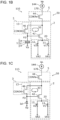
- Fig. 1B is a diagram schematically showing an exemplary circuit configuration of one pixel 110 in the imaging device 100 according to the present embodiment.
- the pixel 110 comprises a photoelectric converting portion 1, an amplifier 2, a band control portion 3, a charge accumulation portion FD, and an output selecting portion 5.
- the photoelectric converting portion 1 detects light and converts the light into signal charge.
- the charge accumulation portion FD accumulates the signal charge generated by the photoelectric converting portion 1.
- the amplifier 2, the band control portion 3, the charge accumulation portion FD, and the output selecting portion 5 form a readout circuit 50.
- the photoelectric converting portion 1 converts light into signal charge.
- the readout circuit 50 reads out the signal charge generated by the photoelectric converting portion 1.
- the photoelectric converting portion 1 comprises, for example, a pixel electrode 1a, the counter electrode 1b, and a photoelectric conversion layer 1c sandwiched between the pixel electrode 1a and the counter electrode 1b.
- the pixel electrode 1a is electrically connected to the charge accumulation portion FD.
- the counter electrode 1b is connected to the accumulation control line 130 shown in Fig. 1A and is electrically connected to the voltage supply circuit 140 through the accumulation control line 130.
- the charge accumulation portion FD is connected to the photoelectric converting portion 1 through a wiring layer.
- the charge accumulation portion FD accumulates the signal charge generated by the photoelectric converting portion 1.
- the charge accumulation portion FD is further connected to an input of the amplifier 2.
- the amplifier 2 amplifies a signal corresponding to the signal charge accumulated in the charge accumulation portion FD and outputs the amplified signal to the band control portion 3 and the output selecting portion 5.
- the amplifier 2 and the band control portion 3 form a feedback circuit 30 via the charge accumulation portion FD.
- the band control portion 3 includes a band control circuit 13. At least three voltages that are different from each other are supplied from a voltage control circuit to the band control circuit 13. Since such voltages are supplied, the band control circuit 13 has a band control function.
- the voltage control circuit is, for example, a portion of the vertical scanning circuit 141.
- the band control circuit 13 applies a band limitation to an output signal of the amplifier 2 to output a signal to the charge accumulation portion FD.
- a signal read out from the charge accumulation portion FD is amplified by the amplifier 2, is subjected to the band limitation by the band control circuit 13, and is fed back to the charge accumulation portion FD.
- the feedback circuit 30 negatively feeds back a signal of the photoelectric converting portion 1 to the charge accumulation portion FD via an amplifying transistor 42.
- the feedback circuit 30 is a circuit that negatively feeds back a potential of the charge accumulation portion FD during a reset operation, which is described below.
- the amplifier 2 has the amplifying transistor 42 and a switching circuit 20, which includes a first switching element 11 and a second switching element 12.
- Transistors in the readout circuit 50 are, for example, N-channel MOSFETs (Metal Oxide Semiconductor Field Effect Transistors). Electrical connection relationships in the readout circuit 50 will be described below.
- the amplifier 2 in the pixel 110 does not have to have the switching circuit 20, and the switching circuit 20 may be included in the peripheral circuitry.
- the charge accumulation portion FD is connected to a gate of the amplifying transistor 42.
- the band control portion 3 includes a band control transistor 46.
- the output selecting portion 5 includes a selecting transistor 44.
- One of a source and a drain of the amplifying transistor 42 is connected to one of a source and a drain of the band control transistor 46 and to one of a source and a drain of the selecting transistor 44.
- the other of the source and the drain of the band control transistor 46 is connected to the charge accumulation portion FD.
- the band control transistor 46 and a capacitance component that is parasitic in the charge accumulation portion FD form an RC filter circuit.
- the amplification-control signal line CON3 is connected to a gate of the band control transistor 46.
- the state of the band control transistor 46 is determined by a voltage of the amplification-control signal line CON3. For example, when the voltage of the amplification-control signal line CON3 is at a high level, the band control transistor 46 is turned on. As a result, the charge accumulation portion FD, the amplifying transistor 42, and the band control transistor 46 form a feedback path.
- the other of the source and the drain of the selecting transistor 44 is connected to the signal-readout signal line 170.
- a gate of the selecting transistor 44 is controlled through the selection-control signal line CON7.
- the state of the selecting transistor 44 is determined by a voltage of the selection-control signal line CON7. For example, when the voltage of the selection-control signal line CON7 is at a high level, the selecting transistor 44 is turned on. As a result, the amplifying transistor 42 and the signal-readout signal line 170 are electrically connected to each other. When the voltage of the selection-control signal line CON7 is at a low level, the selecting transistor 44 is turned off. As a result, the amplifying transistor 42 and the signal-readout signal line 170 are electrically isolated from each other.
- the switching circuit 20 is connected to the other of the source and the drain of the amplifying transistor 42. Specifically, the other of the source and the drain of the amplifying transistor 42 is connected to a first voltage supply VA1 via the first switching element 11. Also, the other of the source and the drain of the amplifying transistor 42 is also connected to a second voltage supply VA2 via the second switching element 12.
- the switching circuit 20 is controlled with control signals V1 and V2 to thereby switch a voltage, applied to the other of the source and the drain of the amplifying transistor 42, to a voltage Va1 or a voltage Va2.
- the voltage Va1 of the first voltage supply VA1 is, for example, a ground voltage GND.
- the voltage Va2 of the second voltage supply VA2 is, for example, a power-supply voltage VDD.
- the switching circuit 20 may be provided for each pixel or may be shared by two or more pixels in order to reduce the number of elements per pixel.
- the output selecting portion 5 is connected to the signal-readout signal line 170.
- the signal-readout signal line 170 is shared by at least two pixels.
- the signal amplified by the amplifier 2 is output to the signal-readout signal line 170 via the output selecting portion 5.
- the constant-current source 144 is connected to the signal-readout signal line 170.
- the selecting transistor 44 When the selecting transistor 44 is on, the selecting transistor 44, the amplifying transistor 42, and the constant-current source 144 form a source follower circuit.
- the signal corresponding to the signal charge accumulated in the charge accumulation portion FD is output to the signal-readout signal line 170 and is read out to outside.
- the constant-current source 144 may be provided for each pixel or may be shared by two or more pixels in order to reduce the number of elements per pixel.
- the photoelectric converting portion 1 is not limited to such a configuration and may be an element, such as a photodiode, having another photoelectric conversion function.
- Fig. 1C is a diagram schematically showing an exemplary circuit configuration of one pixel 115 in the imaging device according to the present embodiment. Compared with the above-described pixel 110, the pixel 115 shown in Fig. 1C differs in that it comprises a photoelectric converting portion 1d instead of the photoelectric converting portion 1. The configuration other than the photoelectric converting portion 1d in the pixel 115 is the same as that of the pixel 110. As shown in Fig. 1C , the pixel 115 comprises the photoelectric converting portion 1d constituted by a photodiode.
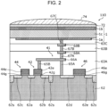
- Fig. 2 is a sectional view schematically showing a device structure of the pixels 110 in the imaging device 100 according to the present embodiment.
- the pixels 110 include a semiconductor substrate 62 that supports the photoelectric converting portions 1.
- the semiconductor substrate 62 is, for example, a silicon substrate.
- each photoelectric converting portion 1 is arranged above the semiconductor substrate 62.
- interlayer insulating layers 63A, 63B, and 63C are stacked on the semiconductor substrate 62, and a stack of the pixel electrode 1a, the photoelectric conversion layer 1c, and the counter electrodes 1b is arranged on the interlayer insulating layer 63C.
- the pixel electrodes 1a are sectioned for the respective pixels, and the pixel electrodes 1a in two adjacent pixels 110 are formed spatially separated from each other, so that two adjacent pixel electrodes 1a are electrically isolated from each other. Also, the photoelectric conversion layer 1c and the counter electrode 1b may be formed so as to extend through two or more pixels 110.
- the signal charge generated by the photoelectric converting portion 1 is accumulated in a charge accumulation node 41 between the gate of the amplifying transistor 42 and the photoelectric converting portion 1.
- the charge accumulation node 41 is one example of the above-described charge accumulation portion FD.
- the pixel electrode 1a is an electrode for reading out the signal charge generated by the photoelectric converting portion 1. At least one pixel electrode 1a exists in each pixel 110. The pixel electrode 1a is electrically connected to a gate electrode 42e of the amplifying transistor 42 and an impurity region 62d.
- the pixel electrode 1a is formed using an electrically conductive material.
- the electrically conductive material is, for example, metal such as aluminum or copper, metal nitride, or polysilicon given electrical conductivity by impurity doping.
- the counter electrode 1b is, for example, a transparent electrode formed of a transparent electrically conductive material.
- the counter electrode 1b is arranged at a light incidence side of the photoelectric converting portion 1. Accordingly, light that is transmitted through the counter electrode 1b is incident on the photoelectric conversion layer 1c.
- the "transparent” herein means transmitting at least part of light in a wavelength range to be detected and does not necessarily have to transmit light in the entire visible-light wavelength range.
- the counter electrode 1b is formed, for example, using transparent conducting oxide (TCO: Transparent Conducting Oxide), such as ITO (Indium Tin Oxide).
- TCO Transparent Conducting Oxide
- ITO Indium Tin Oxide
- the photoelectric conversion layer 1c generates hole-electron pairs, upon receiving incident light.
- a semiconductive inorganic material, a semiconductive organic material, or the like is used as the material of the photoelectric conversion layer 1c.
- the photoelectric conversion layer 1c is, for example, an organic photoelectric conversion film.
- the amplifying transistors 42, the selecting transistors 44, and the band control transistors 46 are formed at the semiconductor substrate 62.
- Each amplifying transistor 42 includes impurity regions 62a and 62b formed in the semiconductor substrate 62, a gate insulating layer 42g located on the semiconductor substrate 62, and the gate electrode 42e located on the gate insulating layer 42g.
- the impurity regions 62a and 62b each function as the drain or the source of the amplifying transistor 42.
- the impurity region 62a and 62b and impurity regions 62c, 62d, and 62e described below are, for example, n-type impurity regions.
- Each selecting transistor 44 includes the impurity regions 62a and 62c formed in the semiconductor substrate 62, a gate insulating layer 44g located on the semiconductor substrate 62, and a gate electrode 44e located on the gate insulating layer 44g.
- the impurity regions 62a and 62c each function as the drain or the source of the selecting transistor 44.
- the amplifying transistor 42 and the selecting transistor 44 share the impurity region 62a, so that the source (or the drain) of the amplifying transistor 42 and the drain (or the source) of the selecting transistor 44 are electrically connected to each other.
- Each band control transistor 46 includes the impurity regions 62d and 62e formed in the semiconductor substrate 62, a gate insulating layer 46g located on the semiconductor substrate 62, and a gate electrode 46e located on the gate insulating layer 46g.
- the impurity regions 62d and 62e each function as the drain or the source of the band control transistor 46.
- a plug 67B and a wire 68B are formed in the interlayer insulating layer 63B, and a plug 67C is formed in the interlayer insulating layer 63C, so that the wire 66A and the pixel electrode 1a are electrically connected to each other.
- the contact plugs 65A and 65B, the wire 66A, the plug 67A, the wire 68A, the plug 67B, the wire 68B, and the plug 67C are typically composed of metal.
- a color filter 72 is arranged on the counter electrode 1b. Also, a microlens 74 is arranged on the color filter 72. Although not illustrated, a protective layer for protecting the photoelectric converting portion 1 may be arranged between the color filter 72 and the microlens 74.
- the material of the protective layer is, for example, SiON, AlO, or the like.
- the imaging device 100 as described above can be manufactured using a typical semiconductor manufacturing process.
- the imaging device 100 can be manufactured utilizing various types of silicon semiconductor process.
- Fig. 3 is a diagram schematically showing an exemplary circuit configuration of one pixel 110A in the imaging device according to the present embodiment.
- the pixel 110A shown in Fig. 3 differs in that it comprises a band control portion 3A instead of the band control portion 3. Points that differ from the pixel 110 will be mainly described below, and descriptions of common points will be omitted or briefly given.
- the amplifier 2 In the pixel 110A, the amplifier 2, the band control portion 3A, the charge accumulation portion FD, and the output selecting portion 5 form a readout circuit 50A.
- a feedback circuit 30A negatively feeds back a signal from the photoelectric converting portion 1 to the charge accumulation portion FD via the amplifying transistor 42.
- the feedback circuit 30A is a circuit for negatively feeding back the potential of the charge accumulation portion FD during a reset operation, which is described below.
- the band control portion 3A includes a band control circuit 13A and a reset circuit 14A.
- the band control circuit 13A is a circuit for reducing reset noise that occurs during a reset operation, which is described below.
- the band control circuit 13A includes a band control transistor 46A, a first capacitive element 9, and a second capacitive element 10.
- the "capacitive elements” as used herein each refer to a structure in which a dielectric, such as an insulating film, is interposed between electrodes.
- the "electrodes” are not limited to electrodes formed of metal and are broadly construed as including a polysilicon layer and so on. The electrodes may be part of a semiconductor substrate.
- the first capacitive element 9 and the second capacitive element 10 may be, for example, MIM (metal insulator metal) capacitors or MIS (metal insulator semiconductor) capacitors.
- the reset circuit 14A includes a reset transistor 48.
- the gate of the amplifying transistor 42 is connected to the charge accumulation portion FD.
- One of the source and the drain of the amplifying transistor 42 is connected to one of a source and a drain of the band control transistor 46A.
- One of the source and the drain of the amplifying transistor 42 is also connected to one of the source and the drain of the selecting transistor 44.
- the other of the source and the drain of the band control transistor 46A is connected to one end of the first capacitive element 9.
- a reference voltage VR1 is applied to the other end of the first capacitive element 9.
- the band control transistor 46A and the first capacitive element 9 form an RC filter circuit.
- the signal charge generated in the photoelectric conversion layer 1c is collected by the pixel electrodes 1a.
- a LOW voltage is applied to the counter electrode 1b, the voltage across the counter electrode 1b and the pixel electrodes 1a is changed to a low voltage V L, so that the sensitivity of the organic photoelectric conversion film decreases, and the photoelectric conversion is stopped. That is, in a state in which the pixel electrodes 1a provided in the respective pixels 110 are set to the reset voltage VRST, when the HIGH voltage is supplied to the counter electrode 1b, which is common to all the pixels, the exposure operation is started, and when the LOW voltage is supplied to the counter electrode 1b, the exposure operation is stopped. Also, at this point in time, the voltage of the amplification-control signal line CON3 shown in Fig.
- the potential of the charge accumulation portion FD is initialized.
- the voltage of the amplification-control signal line CON3 is set to, for example, an intermediate voltage between the high level and the low level.
- the reset noise is reduced.
- the voltage of the amplification-control signal line CON3 is set to the low level to turn off the band control transistor 46. As a result, the reset noise is reduced, and also the potential of the charge accumulation portion FD is initialized.
- This readout operation is performed in a state in which signal charge in the exposure operation is accumulated in the charge accumulation portion FD and in a state in which the reset operation is completed on the pixel and the reset voltage VRST is set for the pixel electrode.
- a readout operation performed in a state in which the signal charge in the exposure operation is accumulated in the charge accumulation portion FD is referred to as a “signal readout operation”
- a readout operation performed in a state in which the reset voltage VRST is set for the pixel electrode is referred to as a "reset-signal readout operation”.
- Fig. 5A is a timing chart for describing one example of operations in the imaging device according to the comparative example.
- Fig. 5B is a flowchart showing one example of the operations in the imaging device according to the comparative example.
- a reset operation before an exposure operation needs to be first performed on all the pixels 110, and thus, in a reset operation period A, the control circuit in the imaging device according to the comparative example causes the plurality of pixels 110 in all the rows from the 0 th row to the n th row to perform the reset operation for at least each row (S111).
- reset noise e.g., kTC noise
- the reset operation is performed, as described above.
- the control circuit in the imaging device applies the HIGH voltage to the counter electrode 1b to cause the plurality of pixels 110 to perform the exposure operation in an exposure operation period B (S112).
- the exposure operation is performed on at least two or more pixels 110 of the pixels 110 at a time.
- the control circuit in the imaging device causes the pixels 110 belonging to all the rows from the 0 th row to the n th row to perform a signal readout operation for at least each row, perform, after the signal readout operation, the reset operation again on all the pixels 110 from which signals were read out, and perform, after the reset operation, the reset-signal readout operation again on all the pixels 110 (S113).
- the reset-signal readout operation in a state in which noise in all the pixels 110 from which the signals were read out is reduced, and the reset voltage VRST is set, a readout operation of the reset signals is performed for at least each row.
- the control circuit in the imaging device receives an external trigger signal, determines an exposure starting time, and causes the plurality of pixels 110 to perform a reset operation, an exposure operation, and a signal readout operation (S114 to S117). Operations that are similar to those in steps S111 to S113 are performed in steps S115 to S117.
- a reset operation on all the pixels 110 to be exposed is needed for at least each row in a period from when the trigger signal is received in step S114 and before the exposure operation in step 116 is performed, and thus, a long waiting time T1 occurs from when the external trigger signal is received until the exposure operation is started.
- Fig. 5C is a flowchart showing another example of the operations in the imaging device according to the comparative example.
- the control circuit in the imaging device according to the comparative example first receives an external trigger signal and causes the plurality of pixels 110 to perform a reset operation, an exposure operation, and a signal readout operation (S121 to S124). Operations that are similar to those in steps S114 to S117 described above are performed in steps S121 to S124.
- the imaging device according to the comparative example may determine the exposure-operation starting time upon receiving the external trigger signal, after performing a first round of imaging for initialization, as shown in Fig. 5B , or may determine the exposure-operation starting time at the beginning upon receiving the external trigger signal, as shown in Fig. 5C .
- the imaging device according to the comparative example may repeat the exposure-operation timing control according to the external trigger signal and internal continuous scanning.
- the imaging device 100 operations of the imaging device 100 according to the present embodiment which solves the above-described problem will be described using Figs. 6A to 7 .
- the description below will be given of an example in which the pixels 110 in the imaging device 100 constitute a pixel array of "0 th row to n th row ⁇ 0 th column to m th column".
- the imaging device 100 may comprise the pixels 110A or 115 instead of the pixels 110.
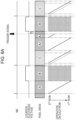
- Fig. 6A is a timing chart for describing one example of operations in the imaging device 100 according to the present embodiment.
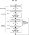
- Fig. 6B is a flowchart showing one example of operations in the imaging device 100 according to the present embodiment.
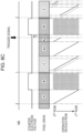
- Fig. 6C is a timing chart for describing another example of the operations in the imaging device 100 according to the present embodiment.
- Figs. 6A and 6C each show a timing of a trigger signal, a timing of falling (or rising) of a vertical synchronization signal VD, time-series changes in the magnitude of a voltage applied to the counter electrode 1b (i.e., a bias voltage applied to the photoelectric conversion layer 1c) of the photoelectric converting portions 1, drive of all the plurality of pixels 110, a reset operation on each row of the pixel array of the pixels 110, a signal readout operation, and an exposure operation.
- a voltage applied to the counter electrode 1b i.e., a bias voltage applied to the photoelectric conversion layer 1c
- the control circuit in the imaging device 100 applies the HIGH voltage to the counter electrode 1b in an exposure operation period B to cause the pixels 110 to perform the exposure operation (S12).
- the exposure operation is simultaneously performed on at least two or more pixels 110 of the plurality of pixels 110.
- the exposure operation may be simultaneously performed on all the pixels 110.
- the control circuit in the imaging device 100 causes the pixels 110 belonging to all the rows from the 0 th row to the n th row to perform a signal readout operation on accumulated pixel signals for at least each row, to perform, after the readout, a reset operation on all the pixels 110 from which the signals were read out, and to perform, after the reset operation, a reset-signal readout operation on all the pixels 110 (S13).
- a reset-signal readout operation in a state in which noise in all the pixels 110 from which the signals were read out is reduced, and the reset voltage VRST is set, a readout operation on reset signals is performed for at least each row.
- a pre-reset operation period A2 provision of a period (a pre-reset operation period A2) in which the reset operation for at least each row is repeated after the readout of the reset signals in step S13 makes it possible to reduce the waiting time from when the external trigger signal is received until the exposure operation is started.
- the control circuit in the imaging device 100 causes the plurality of pixels 110 to perform the reset operation for at least each row (S14).
- the reset operation in step S14 is repeated in units of the 0 th row to the n th row until the control circuit receives the trigger signal from outside (S15). That is, the control circuit in the imaging device 100 causes the plurality of pixels 110 to repeatedly perform the reset operation sequentially for each row until the trigger signal is received.
- the control circuit in the imaging device 100 upon receiving the external trigger signal in step S15, performs interrupt processing to cause the reset operation to be stopped up to the end of processing on the pixels 110 in an x th row on which the reset operation is being performed.
- the reset operation in step S14 is repeated in units of the 0 th row to the n th row "a" times and is further performed from the 0 th row to the x th row.
- "a" is an integer greater than or equal to 0.
- the x th row is one of the rows between the 0 th row and the n th row.
- the control circuit in the imaging device 100 causes all the pixels 110 to sequentially perform, for each row, the reset operation for initializing the potentials of the charge accumulation portions FD before the trigger signal for giving an instruction for starting the exposure is received. Also, the control circuit in the imaging device 100 causes the pixels 110 included in the plurality of pixels 110 and belonging to at least one row to perform the reset operation a plurality of times, until the trigger signal is received. As a result, accumulation of signal charge that derives from dark current or the like that causes noise is reduced before the control circuit receives the external trigger signal.
- the control circuit in the imaging device 100 causes at least two or more pixels of the plurality of pixels 110 to perform the exposure operation (S16). Then, the control circuit in the imaging device 100 causes the plurality of pixels 110 to perform a signal readout operation, a reset operation, and a reset-signal readout operation (S17). That is, after receiving the trigger signal, without causing the pixels 110 included in the plurality of pixels 110 and belonging to at least one row to perform the reset operation, the control circuit in the imaging device 100 causes the plurality of pixels 110 to simultaneously perform the exposure operation for accumulating signal charge in the charge accumulation portions FD.
- the control circuit in the imaging device 100 when the control circuit in the imaging device 100 receives the trigger signal in a period in which steps S11 to S13 are executed, that is, in a period before the reset operation is performed on all the pixels 110, the control circuit does not suspend the operations, such as the reset operation. In this case, for example, the control circuit in the imaging device 100 may discard the received trigger signal and may cause the pixels 110 to perform the exposure operation after step S13 without immediately starting the exposure operation. Also, the control circuit in the imaging device 100 may have a circuit configuration in which the trigger signal is not received in a period before the reset operation is performed on all the plurality of pixels 110.
- the imaging device 100 may be provided with the pre-reset operation period A2 after performing a first round of imaging for initialization and may determine the exposure-operation starting time upon receiving the external trigger signal, as shown in Fig. 6B , or may be provided with the pre-reset operation period A2 at the beginning and may determine the exposure-operation starting time upon receiving the external trigger signal, as shown in Fig. 6D . Also, the imaging device 100 may repeat the exposure-operation timing control according to the external trigger signal and internal continuous scanning.
- step S37 the control circuit in the imaging device 100 causes the plurality of pixels 110 to perform a signal readout operation and a reset operation (step S37).
- step S37 operations that are similar to those in step S33 are performed.
- differences from outputs corresponding to a state in which the reset voltage VRST is set are determined to thereby obtain signals corresponding to the amounts of charge accumulated in the charge accumulation portions FD.
- a second embodiment will be described next.
- a description will be given of an imaging device having a stacked structure of at least two layers.
- Fig. 8 is a schematic view showing one example of a configuration of an imaging device 101 according to the present embodiment.
- the imaging device 101 comprises a first substrate 2000 and a second substrate 2100 stacked on the first substrate 2000.
- the first substrate 2000 is located above the second substrate.
- the first substrate 2000 has a pixel array 111.
- the pixel array 111 has, for example, a structure in which the above-described pixels 110, 110A, or 115 are arranged in a matrix.
- the second substrate 2100 has: an analog-to-digital conversion circuit (AD conversion circuit) 2200 that receives signal outputs (specifically, analog signals) from the pixels included in the pixel array 111 and that converts the signal outputs into digital signals; a memory 2400 in which the signals that are converted into the digital signals by the analog-to-digital conversion circuit 2200 are stored; and a computational processing circuit 2300 that performs computational processing on the signals that are converted into the digital signal by the analog-to-digital conversion circuit 2200.
- AD conversion circuit analog-to-digital conversion circuit
- the first substrate 2000 and the second substrate 2100 are electrically connected through connection portions 2500.
- the pixels 110, 110A, or 115 for realizing the above-described imaging device 100 are provided at the first substrate 2000, and a circuit for controlling the counter electrode 1b in the photoelectric converting portions 1 and a circuit for interrupt control logic are provided at the second substrate 2100. Since the circuit for controlling the counter electrode 1b in the photoelectric converting portion 1 and the circuit for the interrupt control logic are provided at the second substrate 2100, a circuit for free control logics can be constructed without being affected by the pixel area of the pixels included in the pixel array 111. In which of the first substrate 2000 and the second substrate 2100 each circuit is provided may be determined depending on the purpose and is not particularly limited.
- the stacked structure of the imaging device 101 is a structure in which two substrates are stacked
- the stacked structure is not limited thereto.
- the stacked structure may be a structure in which three or more substrates are stacked or a structure in which a plurality of sub-substrates are stacked on one substrate.
- the connection portions 2500 for the substrates may be provided for respective columns, as shown in Fig. 8 , may be provided for respective regions, or may be provided for the respective pixels.
- FIG. 9 is a block diagram showing one example of a configuration of a camera system 1000 according to the third embodiment.
- the camera system 1000 comprises; an imaging device 102; an optical system 1001, such as a lens, for focusing light; a camera-signal processing unit 1002 for performing signal processing on data acquired by the imaging device 102 and outputting it as an image or data; and a system controller 1003 for controlling the imaging device 102 and the camera-signal processing unit 1002.
- the optical system 1001 is a lens or the like for focusing light onto an imaging plane of the imaging device 102. Light that is transmitted through the optical system 1001 is incident on the photoelectric converting portions 1 in the imaging device 102 and is photoelectrically converted, so that signal charge is generated.
- the imaging device 100 or 101 according to the embodiment described above is used as the imaging device 102.
- the camera-signal processing unit 1002 functions as a signal processing circuit for processing output signals from the imaging device 102.
- the camera-signal processing unit 1002 performs processing, for example, gamma correction, color interpolation processing, spatial interpolation processing, automatic white balancing, distance measurement computational operation, wavelength information separation, and so on.
- the camera-signal processing unit 1002 is realized by, for example, a DSP (digital signal processor) or the like.
- the system controller 1003 controls the entire camera system 1000.
- the system controller 1003 can be realized by, for example, a microcomputer.
- the camera system 1000 since the camera system 1000 according to the present embodiment employs the imaging device 100 or 101 according to the above-described embodiment as the imaging device 102, it is possible to reduce the delay time from when the external trigger signal is received until an exposure operation on the entire light-receiving plane is started. Therefore, it is possible to provide a camera system 1000 that is high in usability, that is, that has a short waiting time until the start of the exposure operation, that can image what and when the user wants to image, or that can perform high-speed inspection.
- the imaging device and the camera system according to one or more aspects have been described above based on the embodiments, the present disclosure is not limited to those embodiments.
- the reset operation in step S14 is started immediately after the operation in step S13 is finished
- the reset operation may be started with an interval after the operation in step S13 is finished, as long as an image quality needed for the purpose of use is obtained.
- the present disclosure is not limited thereto.
- a reference voltage may be applied from a circuit different from the switching circuits 20 to thereby perform the reset operation on the charge accumulation portion FD.
- the photoelectric converting portion 1 includes the pixel electrodes 1a, the counter electrode 1b, and the photoelectric conversion layer 1c
- the photoelectric converting portion 1 may further include a charge transporting layer or a charge blocking layer between the photoelectric conversion layer 1c and the pixel electrodes 1a or the counter electrode 1b.
- receiving the trigger signal in a period other than the pre-reset operation period is also envisaged in scenes in which the imaging device in the present disclosure is actually used.
- the trigger signal may also be disregarded.
- the imaging device can be utilized for various sensor systems and camera systems, such as digital still cameras, medical cameras, surveillance cameras, vehicle-mounted cameras, digital single-lens reflex cameras, and digital mirrorless single-lens reflex cameras.
Landscapes
- Engineering & Computer Science (AREA)
- Multimedia (AREA)
- Signal Processing (AREA)
- Solid State Image Pick-Up Elements (AREA)
- Transforming Light Signals Into Electric Signals (AREA)
Claims (12)
- Dispositif d'imagerie comprenant :une pluralité de pixels (110 ; 110A ; 115) agencés en réseau dans une matrice (111), la pluralité de pixels (110, 110A, 115) incluant respectivement des portions de conversion photoélectrique (1, 1d) qui convertissent la lumière en charge de signal et des portions d'accumulation de charge (41) qui accumulent la charge de signal ; etun circuit de contrôle,dans lequel le circuit de contrôlecommande aux pixels (110, 110A, 115) d'exécuter séquentiellement, dans chaque rangée ou dans deux ou plusieurs rangées à la fois, une opération de pré-réinitialisation (S14) pour initialiser les potentiels des portions d'accumulation de charge (41), à moins qu'un signal de déclenchement qui donne une instruction de démarrage d'exposition ne soit reçu,commande, après réception (S15) du signal de déclenchement, à la pluralité de pixels (110, 110A, 115) d'exécuter simultanément une opération d'exposition (S16) pour accumuler la charge de signal dans les portions d'accumulation de charge (41) sans commander aux pixels d'exécuter la pré-réinitialisation et tout en arrêtant toute opération de pré-réinitialisation en cours jusqu'à la fin du traitement sur les pixels d'au moins une rangée sur laquelle l'opération de pré-réinitialisation est exécutée, ou en exécutant l'opération de pré-réinitialisation sur certaines rangées additionnelles à partir de ladite au moins une rangée sur laquelle l'opération de pré-réinitialisation est exécutée et en n'exécutant pas l'opération de pré-réinitialisation sur les pixels d'au moins une rangée après réception du signal de déclenchement, etcommande, après avoir exécuté l'opération d'exposition, à la pluralité de pixels d'exécuter (S17) une opération de lecture de signal, une opération de réinitialisation et une opération de lecture de signal de réinitialisation,dans lequel le circuit de contrôle est configuré pour démarrer l'opération de pré-réinitialisation (S14) après l'opération de lecture de signal de réinitialisation (S17) et pour commander l'exécution de l'opération de pré-réinitialisation jusqu'à ce que le signal de déclenchement qui donne l'instruction de démarrage d'exposition soit reçu.
- Dispositif d'imagerie selon la revendication 1, dans lequel, avant la réception du signal de déclenchement, le circuit de contrôle commande aux pixels inclus dans la pluralité de pixels (110, 110A, 115) et appartenant à au moins une rangée d'exécuter plusieurs fois l'opération de pré-réinitialisation.
- Dispositif d'imagerie selon la revendication 1 ou 2, dans lequel le circuit de contrôle commande à la pluralité de pixels d'exécuter de manière répétée l'opération de pré-réinitialisation séquentiellement pour chaque rangée ou pour deux ou plusieurs rangées à la fois, jusqu'à ce que le signal de déclenchement soit reçu.
- Dispositif d'imagerie selon l'une des revendications 1 à 3, dans lequel, après l'opération d'exposition, le circuit de contrôle commande à la pluralité de pixels d'exécuter séquentiellement une opération de lecture pour envoyer des signaux correspondant à la charge de signal accumulée dans les portions d'accumulation de charge (41), l'opération de lecture étant exécutée pour chaque rangée ou pour deux ou plusieurs rangées à la fois à partir d'une rangée à laquelle l'opération de pré-réinitialisation a été démarrée.
- Dispositif d'imagerie selon l'une des revendications 1 à 3, dans lequel le circuit de contrôlecommande à la pluralité de pixels (110, 110A, 115) d'exécuter séquentiellement, pour chaque rangée ou pour deux ou plusieurs rangées à la fois, l'opération de pré-réinitialisation jusqu'à une rangée différente d'une rangée à laquelle l'opération de pré-réinitialisation a été démarrée, etcommande, après l'opération d'exposition, à la pluralité de pixels (110, 110A, 115) d'exécuter séquentiellement une opération de lecture pour envoyer des signaux correspondant à la charge de signal accumulée dans les portions d'accumulation de charge (41), l'opération de lecture étant exécutée pour chaque rangée ou pour deux ou plusieurs rangées à la fois à partir d'une rangée d'un ordre qui suit celui d'une rangée à laquelle l'opération de pré-réinitialisation a été terminée.
- Dispositif d'imagerie selon l'une des revendications 1 à 5, dans lequel chaque pixel de la pluralité de pixels (110, 110A, 115) inclut un circuit de rétroaction (30, 30A) pour une rétroaction négative d'un potentiel de la portion d'accumulation de charge (41) dans l'opération de pré-réinitialisation.
- Dispositif d'imagerie selon l'une des revendications 1 à 6, dans lequel chaque pixel de la pluralité de pixels (110, 110A, 115) inclut un circuit pour réduire le bruit de pré-réinitialisation qui se produit lors de l'opération de pré-réinitialisation.
- Dispositif d'imagerie selon l'une des revendications 1 à 7, dans lequel l'opération de pré-réinitialisation inclut une opération de rétroaction négative des potentiels des portions d'accumulation de charge.
- Dispositif d'imagerie selon l'une des revendications 1 à 8, comprenant en outre :un circuit d'alimentation de tension (120),dans lequel les portions de conversion photoélectrique (1, 1d) incluent une contre-électrode (1b) connectée électriquement au circuit d'alimentation de tension (120), des électrodes de pixel (1a) connectées électriquement aux portions d'accumulation de charge (41), et une couche de conversion photoélectrique (1c) située entre la contre-électrode (1b) et les électrodes de pixel (1a) ; etle circuit de contrôle commande au circuit d'alimentation de tension (120) d'appliquer une tension à la contre-électrode (1b) pour former un champ électrique dans la couche de conversion photoélectrique (1c) pour ainsi commander à la pluralité de pixels (110, 110A, 115) d'exécuter l'opération d'exposition.
- Dispositif d'imagerie selon l'une quelconque des revendications 1 à 9, dans lequel le dispositif d'imagerie obtient un signal correspondant à la quantité de charge de signal générée par conversion photoélectrique durant l'opération d'exposition en déterminant les différences entre une sortie dans l'opération de lecture de signal et une sortie dans l'opération de lecture de signal de réinitialisation.
- Procédé de contrôle d'un dispositif d'imagerie (100, 101, 102) comprenant une pluralité de pixels (110, 110A, 115) agencés en réseau dans une matrice (111), la pluralité de pixels (110, 110A, 115) incluant respectivement des portions de conversion photoélectrique (1, 1d) qui convertissent la lumière en charge de signal et des portions d'accumulation de charge (41) qui accumulent la charge de signal, le procédé comprenant les étapes suivantes :exécution d'une opération de pré-réinitialisation (S14 ; S22) pour initialiser les potentiels des portions d'accumulation de charge (41), séquentiellement dans chaque rangée ou dans deux ou plusieurs rangées à la fois, sur les pixels (110, 110A, 115), à moins qu'un signal de déclenchement qui donne une instruction de démarrage d'exposition ne soit reçu ;après réception du signal de déclenchement (S15 ; S23), exécution d'une opération d'exposition (S16 ; S24) pour accumuler la charge de signal dans les portions d'accumulation de charge (41) simultanément sur la pluralité de pixels (110, 110A, 115) sans exécuter l'opération de pré-réinitialisation sur les pixels et tout en arrêtant toute opération de pré-réinitialisation en cours jusqu'à la fin du traitement sur les pixels d'au moins une rangée sur laquelle l'opération de pré-réinitialisation est exécutée, ou en exécutant l'opération de pré-réinitialisation sur certaines rangées additionnelles à partir de ladite au moins une rangée sur laquelle l'opération de pré-réinitialisation est exécutée et en n'exécutant pas l'opération de pré-réinitialisation sur les pixels d'au moins une rangée après réception du signal de déclenchement ; etcommande (S17 ; S25), après avoir exécuté l'opération d'exposition (S16 ; S24), à la pluralité de pixels d'exécuter une opération de lecture de signal, une opération de réinitialisation et une opération de lecture de signal de réinitialisation,dans lequel l'opération de pré-réinitialisation est démarrée après l'opération de lecture de signal de réinitialisation et est exécutée jusqu'à ce que le signal de déclenchement qui donne l'instruction de démarrage d'exposition soit reçu.
- Procédé de contrôle selon la revendication 11, dans lequel l'opération de pré-réinitialisation (S14 ; S22) inclut une opération de rétroaction négative des potentiels des portions d'accumulation de charge (41).
Applications Claiming Priority (2)
| Application Number | Priority Date | Filing Date | Title |
|---|---|---|---|
| JP2019216966 | 2019-11-29 | ||
| PCT/JP2020/032206 WO2021106294A1 (fr) | 2019-11-29 | 2020-08-26 | Dispositif de capture d'image et procédé de commande |
Publications (3)
| Publication Number | Publication Date |
|---|---|
| EP4068362A1 EP4068362A1 (fr) | 2022-10-05 |
| EP4068362A4 EP4068362A4 (fr) | 2023-01-11 |
| EP4068362B1 true EP4068362B1 (fr) | 2025-07-09 |
Family
ID=76130450
Family Applications (1)
| Application Number | Title | Priority Date | Filing Date |
|---|---|---|---|
| EP20894775.4A Active EP4068362B1 (fr) | 2019-11-29 | 2020-08-26 | Dispositif de capture d'image et procédé de commande |
Country Status (5)
| Country | Link |
|---|---|
| US (1) | US12348681B2 (fr) |
| EP (1) | EP4068362B1 (fr) |
| JP (1) | JP7599135B2 (fr) |
| CN (1) | CN114631308B (fr) |
| WO (1) | WO2021106294A1 (fr) |
Families Citing this family (1)
| Publication number | Priority date | Publication date | Assignee | Title |
|---|---|---|---|---|
| CN120916073B (zh) * | 2025-10-10 | 2026-02-03 | 创视半导体(杭州)有限公司 | 一种提高图像传感器帧率的方法 |
Family Cites Families (15)
| Publication number | Priority date | Publication date | Assignee | Title |
|---|---|---|---|---|
| JP2001177084A (ja) | 1999-12-14 | 2001-06-29 | Olympus Optical Co Ltd | 固体撮像素子 |
| JP4025836B2 (ja) * | 2004-10-07 | 2007-12-26 | コニカミノルタオプト株式会社 | 撮像装置及び携帯通信機器 |
| JP2008028516A (ja) | 2006-07-19 | 2008-02-07 | Olympus Corp | カメラシステム |
| JP2010129705A (ja) | 2008-11-27 | 2010-06-10 | Nikon Corp | 固体撮像素子及びその製造方法 |
| JP2010166159A (ja) | 2009-01-13 | 2010-07-29 | Olympus Imaging Corp | カメラ、カメラのぶれ補正方法 |
| JP5331557B2 (ja) * | 2009-04-23 | 2013-10-30 | オリンパス株式会社 | 固体撮像装置及びカメラシステム |
| JP2012129817A (ja) * | 2010-12-15 | 2012-07-05 | Canon Inc | 撮像装置及び撮像素子の制御方法 |
| JP2014078870A (ja) | 2012-10-11 | 2014-05-01 | Fujifilm Corp | 固体撮像素子および撮像装置 |
| CN104823442B (zh) * | 2012-12-05 | 2018-03-30 | 松下知识产权经营株式会社 | 固体摄像装置 |
| US9737271B2 (en) * | 2014-04-09 | 2017-08-22 | Canon Kabushiki Kaisha | Radiation imaging apparatus and control method of the same |
| CN111901540B (zh) * | 2014-12-26 | 2023-05-23 | 松下知识产权经营株式会社 | 摄像装置 |
| CN112929586B (zh) * | 2015-12-03 | 2024-12-06 | 松下知识产权经营株式会社 | 摄像装置 |
| JP6646824B2 (ja) | 2016-01-22 | 2020-02-14 | パナソニックIpマネジメント株式会社 | 撮像装置 |
| CN109792496B (zh) * | 2016-09-23 | 2021-03-02 | 富士胶片株式会社 | 摄像装置、摄像装置的动作方法、记录介质 |
| CN110463185B (zh) | 2017-03-22 | 2021-09-03 | 富士胶片株式会社 | 摄像装置、摄像方法及存储介质 |
-
2020
- 2020-08-26 EP EP20894775.4A patent/EP4068362B1/fr active Active
- 2020-08-26 JP JP2021561164A patent/JP7599135B2/ja active Active
- 2020-08-26 CN CN202080076398.0A patent/CN114631308B/zh active Active
- 2020-08-26 WO PCT/JP2020/032206 patent/WO2021106294A1/fr not_active Ceased
-
2022
- 2022-04-26 US US17/660,829 patent/US12348681B2/en active Active
Also Published As
| Publication number | Publication date |
|---|---|
| CN114631308B (zh) | 2026-03-31 |
| JP7599135B2 (ja) | 2024-12-13 |
| WO2021106294A1 (fr) | 2021-06-03 |
| EP4068362A4 (fr) | 2023-01-11 |
| JPWO2021106294A1 (fr) | 2021-06-03 |
| US20220256106A1 (en) | 2022-08-11 |
| CN114631308A (zh) | 2022-06-14 |
| EP4068362A1 (fr) | 2022-10-05 |
| US12348681B2 (en) | 2025-07-01 |
Similar Documents
| Publication | Publication Date | Title |
|---|---|---|
| JP7617521B2 (ja) | 撮像装置 | |
| US12021094B2 (en) | Imaging device including photoelectric converters and capacitor | |
| US11482558B2 (en) | Imaging device including unit pixel cell | |
| US9654712B2 (en) | Pixels with a global shutter and high dynamic range | |
| CN204633945U (zh) | 图像传感器、成像系统和处理器系统 | |
| US10559614B2 (en) | Dual conversion gain circuitry with buried channels | |
| KR100928101B1 (ko) | 이미지 센서용 멀티 포인트 상관 샘플링 | |
| TWI395325B (zh) | 提供共用像素直閘架構之裝置 | |
| US7782383B2 (en) | Noise and parasitic capacitance reduction for 1T pixel CMOS image sensors | |
| US20090251556A1 (en) | Solid-state imaging device, signal processing method of solid-state imaging device, and electronic apparatus | |
| US10834342B2 (en) | Image sensors with reduced noise | |
| US10791294B2 (en) | Image sensors having capacitively coupled pixels | |
| CN112449135B (zh) | 具有可调放大器电路的成像系统 | |
| US9007505B2 (en) | Image sensor with transfer transistors whose on periods are controlled by timing signals based on transistor transfer efficiencies | |
| US20170347049A1 (en) | Solid state imaging device and imaging system | |
| US20220102401A1 (en) | Image sensing device | |
| KR20130134506A (ko) | 유기 이미지 센서 및 그 제조방법 | |
| US20220068987A1 (en) | Image sensing device | |
| US11722802B2 (en) | Imaging systems with adjustable amplifier circuitry | |
| US12348681B2 (en) | Imaging device and control method | |
| CN112291490A (zh) | 成像系统及生成具有降低的暗电流噪声的图像信号的方法 | |
| TWI382750B (zh) | 影像感測器中暗電流減少之方法及裝置 | |
| US20230007195A1 (en) | Imaging device and imaging method | |
| KR20260064259A (ko) | 이미지 센싱 장치 | |
| KR20250036452A (ko) | 이미지 센싱 장치 |
Legal Events
| Date | Code | Title | Description |
|---|---|---|---|
| STAA | Information on the status of an ep patent application or granted ep patent |
Free format text: STATUS: THE INTERNATIONAL PUBLICATION HAS BEEN MADE |
|
| PUAI | Public reference made under article 153(3) epc to a published international application that has entered the european phase |
Free format text: ORIGINAL CODE: 0009012 |
|
| STAA | Information on the status of an ep patent application or granted ep patent |
Free format text: STATUS: REQUEST FOR EXAMINATION WAS MADE |
|
| 17P | Request for examination filed |
Effective date: 20220627 |
|
| AK | Designated contracting states |
Kind code of ref document: A1 Designated state(s): AL AT BE BG CH CY CZ DE DK EE ES FI FR GB GR HR HU IE IS IT LI LT LU LV MC MK MT NL NO PL PT RO RS SE SI SK SM TR |
|
| A4 | Supplementary search report drawn up and despatched |
Effective date: 20221213 |
|
| RIC1 | Information provided on ipc code assigned before grant |
Ipc: H04N 5/374 20110101ALI20221207BHEP Ipc: H04N 5/353 20110101ALI20221207BHEP Ipc: H04N 5/3745 20110101ALI20221207BHEP Ipc: H04N 5/363 20110101ALI20221207BHEP Ipc: H04N 5/361 20110101ALI20221207BHEP Ipc: H04N 5/357 20110101ALI20221207BHEP Ipc: H01L 27/146 20060101AFI20221207BHEP |
|
| DAV | Request for validation of the european patent (deleted) | ||
| DAX | Request for extension of the european patent (deleted) | ||
| STAA | Information on the status of an ep patent application or granted ep patent |
Free format text: STATUS: EXAMINATION IS IN PROGRESS |
|
| 17Q | First examination report despatched |
Effective date: 20240404 |
|
| REG | Reference to a national code |
Ref country code: DE Free format text: PREVIOUS MAIN CLASS: H01L0027146000 Ipc: H04N0025616000 Ref country code: DE Ref legal event code: R079 Ref document number: 602020054384 Country of ref document: DE Free format text: PREVIOUS MAIN CLASS: H01L0027146000 Ipc: H04N0025616000 |
|
| GRAP | Despatch of communication of intention to grant a patent |
Free format text: ORIGINAL CODE: EPIDOSNIGR1 |
|
| STAA | Information on the status of an ep patent application or granted ep patent |
Free format text: STATUS: GRANT OF PATENT IS INTENDED |
|
| RIC1 | Information provided on ipc code assigned before grant |
Ipc: H04N 25/63 20230101ALI20250313BHEP Ipc: H04N 25/65 20230101ALI20250313BHEP Ipc: H04N 25/616 20230101AFI20250313BHEP |
|
| INTG | Intention to grant announced |
Effective date: 20250328 |
|
| GRAS | Grant fee paid |
Free format text: ORIGINAL CODE: EPIDOSNIGR3 |
|
| GRAA | (expected) grant |
Free format text: ORIGINAL CODE: 0009210 |
|
| STAA | Information on the status of an ep patent application or granted ep patent |
Free format text: STATUS: THE PATENT HAS BEEN GRANTED |
|
| AK | Designated contracting states |
Kind code of ref document: B1 Designated state(s): AL AT BE BG CH CY CZ DE DK EE ES FI FR GB GR HR HU IE IS IT LI LT LU LV MC MK MT NL NO PL PT RO RS SE SI SK SM TR |
|
| REG | Reference to a national code |
Ref country code: GB Ref legal event code: FG4D |
|
| REG | Reference to a national code |
Ref country code: CH Ref legal event code: EP |
|
| REG | Reference to a national code |
Ref country code: IE Ref legal event code: FG4D |
|
| REG | Reference to a national code |
Ref country code: DE Ref legal event code: R096 Ref document number: 602020054384 Country of ref document: DE |
|
| PGFP | Annual fee paid to national office [announced via postgrant information from national office to epo] |
Ref country code: DE Payment date: 20250820 Year of fee payment: 6 |
|
| REG | Reference to a national code |
Ref country code: NL Ref legal event code: MP Effective date: 20250709 |
|
| PG25 | Lapsed in a contracting state [announced via postgrant information from national office to epo] |
Ref country code: PT Free format text: LAPSE BECAUSE OF FAILURE TO SUBMIT A TRANSLATION OF THE DESCRIPTION OR TO PAY THE FEE WITHIN THE PRESCRIBED TIME-LIMIT Effective date: 20251110 |
|
| PG25 | Lapsed in a contracting state [announced via postgrant information from national office to epo] |
Ref country code: NL Free format text: LAPSE BECAUSE OF FAILURE TO SUBMIT A TRANSLATION OF THE DESCRIPTION OR TO PAY THE FEE WITHIN THE PRESCRIBED TIME-LIMIT Effective date: 20250709 |
|
| REG | Reference to a national code |
Ref country code: AT Ref legal event code: MK05 Ref document number: 1812987 Country of ref document: AT Kind code of ref document: T Effective date: 20250709 |
|
| PG25 | Lapsed in a contracting state [announced via postgrant information from national office to epo] |
Ref country code: IS Free format text: LAPSE BECAUSE OF FAILURE TO SUBMIT A TRANSLATION OF THE DESCRIPTION OR TO PAY THE FEE WITHIN THE PRESCRIBED TIME-LIMIT Effective date: 20251109 |
|
| PG25 | Lapsed in a contracting state [announced via postgrant information from national office to epo] |
Ref country code: NO Free format text: LAPSE BECAUSE OF FAILURE TO SUBMIT A TRANSLATION OF THE DESCRIPTION OR TO PAY THE FEE WITHIN THE PRESCRIBED TIME-LIMIT Effective date: 20251009 |
|
| REG | Reference to a national code |
Ref country code: LT Ref legal event code: MG9D |
|
| PG25 | Lapsed in a contracting state [announced via postgrant information from national office to epo] |
Ref country code: AT Free format text: LAPSE BECAUSE OF FAILURE TO SUBMIT A TRANSLATION OF THE DESCRIPTION OR TO PAY THE FEE WITHIN THE PRESCRIBED TIME-LIMIT Effective date: 20250709 |
|
| PG25 | Lapsed in a contracting state [announced via postgrant information from national office to epo] |
Ref country code: FI Free format text: LAPSE BECAUSE OF FAILURE TO SUBMIT A TRANSLATION OF THE DESCRIPTION OR TO PAY THE FEE WITHIN THE PRESCRIBED TIME-LIMIT Effective date: 20250709 |
|
| PG25 | Lapsed in a contracting state [announced via postgrant information from national office to epo] |
Ref country code: HR Free format text: LAPSE BECAUSE OF FAILURE TO SUBMIT A TRANSLATION OF THE DESCRIPTION OR TO PAY THE FEE WITHIN THE PRESCRIBED TIME-LIMIT Effective date: 20250709 |
|
| PG25 | Lapsed in a contracting state [announced via postgrant information from national office to epo] |
Ref country code: GR Free format text: LAPSE BECAUSE OF FAILURE TO SUBMIT A TRANSLATION OF THE DESCRIPTION OR TO PAY THE FEE WITHIN THE PRESCRIBED TIME-LIMIT Effective date: 20251010 |
|
| PG25 | Lapsed in a contracting state [announced via postgrant information from national office to epo] |
Ref country code: SE Free format text: LAPSE BECAUSE OF FAILURE TO SUBMIT A TRANSLATION OF THE DESCRIPTION OR TO PAY THE FEE WITHIN THE PRESCRIBED TIME-LIMIT Effective date: 20250709 |
|
| PG25 | Lapsed in a contracting state [announced via postgrant information from national office to epo] |
Ref country code: LV Free format text: LAPSE BECAUSE OF FAILURE TO SUBMIT A TRANSLATION OF THE DESCRIPTION OR TO PAY THE FEE WITHIN THE PRESCRIBED TIME-LIMIT Effective date: 20250709 |
|
| PG25 | Lapsed in a contracting state [announced via postgrant information from national office to epo] |
Ref country code: PL Free format text: LAPSE BECAUSE OF FAILURE TO SUBMIT A TRANSLATION OF THE DESCRIPTION OR TO PAY THE FEE WITHIN THE PRESCRIBED TIME-LIMIT Effective date: 20250709 Ref country code: BG Free format text: LAPSE BECAUSE OF FAILURE TO SUBMIT A TRANSLATION OF THE DESCRIPTION OR TO PAY THE FEE WITHIN THE PRESCRIBED TIME-LIMIT Effective date: 20250709 |
|
| PG25 | Lapsed in a contracting state [announced via postgrant information from national office to epo] |
Ref country code: RS Free format text: LAPSE BECAUSE OF FAILURE TO SUBMIT A TRANSLATION OF THE DESCRIPTION OR TO PAY THE FEE WITHIN THE PRESCRIBED TIME-LIMIT Effective date: 20251009 |
|
| PG25 | Lapsed in a contracting state [announced via postgrant information from national office to epo] |
Ref country code: ES Free format text: LAPSE BECAUSE OF FAILURE TO SUBMIT A TRANSLATION OF THE DESCRIPTION OR TO PAY THE FEE WITHIN THE PRESCRIBED TIME-LIMIT Effective date: 20250709 |
|
| PG25 | Lapsed in a contracting state [announced via postgrant information from national office to epo] |
Ref country code: RO Free format text: LAPSE BECAUSE OF FAILURE TO SUBMIT A TRANSLATION OF THE DESCRIPTION OR TO PAY THE FEE WITHIN THE PRESCRIBED TIME-LIMIT Effective date: 20250709 |
|
| REG | Reference to a national code |
Ref country code: CH Ref legal event code: H13 Free format text: ST27 STATUS EVENT CODE: U-0-0-H10-H13 (AS PROVIDED BY THE NATIONAL OFFICE) Effective date: 20260324 |
|
| PG25 | Lapsed in a contracting state [announced via postgrant information from national office to epo] |
Ref country code: SM Free format text: LAPSE BECAUSE OF FAILURE TO SUBMIT A TRANSLATION OF THE DESCRIPTION OR TO PAY THE FEE WITHIN THE PRESCRIBED TIME-LIMIT Effective date: 20250709 |
|
| PG25 | Lapsed in a contracting state [announced via postgrant information from national office to epo] |
Ref country code: DK Free format text: LAPSE BECAUSE OF FAILURE TO SUBMIT A TRANSLATION OF THE DESCRIPTION OR TO PAY THE FEE WITHIN THE PRESCRIBED TIME-LIMIT Effective date: 20250709 |
|
| PG25 | Lapsed in a contracting state [announced via postgrant information from national office to epo] |
Ref country code: LU Free format text: LAPSE BECAUSE OF NON-PAYMENT OF DUE FEES Effective date: 20250826 Ref country code: IT Free format text: LAPSE BECAUSE OF FAILURE TO SUBMIT A TRANSLATION OF THE DESCRIPTION OR TO PAY THE FEE WITHIN THE PRESCRIBED TIME-LIMIT Effective date: 20250709 |
|
| PG25 | Lapsed in a contracting state [announced via postgrant information from national office to epo] |
Ref country code: CZ Free format text: LAPSE BECAUSE OF FAILURE TO SUBMIT A TRANSLATION OF THE DESCRIPTION OR TO PAY THE FEE WITHIN THE PRESCRIBED TIME-LIMIT Effective date: 20250709 Ref country code: CH Free format text: LAPSE BECAUSE OF NON-PAYMENT OF DUE FEES Effective date: 20250831 |
|
| PG25 | Lapsed in a contracting state [announced via postgrant information from national office to epo] |
Ref country code: SK Free format text: LAPSE BECAUSE OF FAILURE TO SUBMIT A TRANSLATION OF THE DESCRIPTION OR TO PAY THE FEE WITHIN THE PRESCRIBED TIME-LIMIT Effective date: 20250709 Ref country code: EE Free format text: LAPSE BECAUSE OF FAILURE TO SUBMIT A TRANSLATION OF THE DESCRIPTION OR TO PAY THE FEE WITHIN THE PRESCRIBED TIME-LIMIT Effective date: 20250709 |
|
| PLBE | No opposition filed within time limit |
Free format text: ORIGINAL CODE: 0009261 |
|
| STAA | Information on the status of an ep patent application or granted ep patent |
Free format text: STATUS: NO OPPOSITION FILED WITHIN TIME LIMIT |