EP4068630A1 - Takterzeugungsschaltung und verriegelung unter verwendung derselben sowie rechnervorrichtung - Google Patents
Takterzeugungsschaltung und verriegelung unter verwendung derselben sowie rechnervorrichtung Download PDFInfo
- Publication number
- EP4068630A1 EP4068630A1 EP20908872.3A EP20908872A EP4068630A1 EP 4068630 A1 EP4068630 A1 EP 4068630A1 EP 20908872 A EP20908872 A EP 20908872A EP 4068630 A1 EP4068630 A1 EP 4068630A1
- Authority
- EP
- European Patent Office
- Prior art keywords
- latch
- electrically connected
- circuit
- inverter
- clock generation
- Prior art date
- Legal status (The legal status is an assumption and is not a legal conclusion. Google has not performed a legal analysis and makes no representation as to the accuracy of the status listed.)
- Pending
Links
Images




Classifications
-
- H—ELECTRICITY
- H03—ELECTRONIC CIRCUITRY
- H03K—PULSE TECHNIQUE
- H03K3/00—Circuits for generating electric pulses; Monostable, bistable or multistable circuits
- H03K3/02—Generators characterised by the type of circuit or by the means used for producing pulses
- H03K3/023—Generators characterised by the type of circuit or by the means used for producing pulses by the use of differential amplifiers or comparators, with internal or external positive feedback
- H03K3/0233—Bistable circuits
-
- H—ELECTRICITY
- H03—ELECTRONIC CIRCUITRY
- H03K—PULSE TECHNIQUE
- H03K3/00—Circuits for generating electric pulses; Monostable, bistable or multistable circuits
- H03K3/01—Details
- H03K3/012—Modifications of generator to improve response time or to decrease power consumption
-
- G—PHYSICS
- G06—COMPUTING OR CALCULATING; COUNTING
- G06F—ELECTRIC DIGITAL DATA PROCESSING
- G06F1/00—Details not covered by groups G06F3/00 - G06F13/00 and G06F21/00
- G06F1/04—Generating or distributing clock signals or signals derived directly therefrom
- G06F1/06—Clock generators producing several clock signals
-
- G—PHYSICS
- G06—COMPUTING OR CALCULATING; COUNTING
- G06F—ELECTRIC DIGITAL DATA PROCESSING
- G06F1/00—Details not covered by groups G06F3/00 - G06F13/00 and G06F21/00
- G06F1/04—Generating or distributing clock signals or signals derived directly therefrom
- G06F1/10—Distribution of clock signals, e.g. skew
-
- H—ELECTRICITY
- H03—ELECTRONIC CIRCUITRY
- H03K—PULSE TECHNIQUE
- H03K19/00—Logic circuits, i.e. having at least two inputs acting on one output; Inverting circuits
- H03K19/20—Logic circuits, i.e. having at least two inputs acting on one output; Inverting circuits characterised by logic function, e.g. AND, OR, NOR, NOT circuits
-
- H—ELECTRICITY
- H03—ELECTRONIC CIRCUITRY
- H03K—PULSE TECHNIQUE
- H03K3/00—Circuits for generating electric pulses; Monostable, bistable or multistable circuits
- H03K3/01—Details
- H03K3/017—Adjustment of width or dutycycle of pulses
-
- H—ELECTRICITY
- H03—ELECTRONIC CIRCUITRY
- H03K—PULSE TECHNIQUE
- H03K3/00—Circuits for generating electric pulses; Monostable, bistable or multistable circuits
- H03K3/02—Generators characterised by the type of circuit or by the means used for producing pulses
- H03K3/027—Generators characterised by the type of circuit or by the means used for producing pulses by the use of logic circuits, with internal or external positive feedback
-
- H—ELECTRICITY
- H03—ELECTRONIC CIRCUITRY
- H03K—PULSE TECHNIQUE
- H03K3/00—Circuits for generating electric pulses; Monostable, bistable or multistable circuits
- H03K3/02—Generators characterised by the type of circuit or by the means used for producing pulses
- H03K3/26—Generators characterised by the type of circuit or by the means used for producing pulses by the use, as active elements, of bipolar transistors with internal or external positive feedback
- H03K3/28—Generators characterised by the type of circuit or by the means used for producing pulses by the use, as active elements, of bipolar transistors with internal or external positive feedback using means other than a transformer for feedback
- H03K3/281—Generators characterised by the type of circuit or by the means used for producing pulses by the use, as active elements, of bipolar transistors with internal or external positive feedback using means other than a transformer for feedback using at least two transistors so coupled that the input of one is derived from the output of another, e.g. multivibrator
- H03K3/286—Generators characterised by the type of circuit or by the means used for producing pulses by the use, as active elements, of bipolar transistors with internal or external positive feedback using means other than a transformer for feedback using at least two transistors so coupled that the input of one is derived from the output of another, e.g. multivibrator bistable
- H03K3/288—Generators characterised by the type of circuit or by the means used for producing pulses by the use, as active elements, of bipolar transistors with internal or external positive feedback using means other than a transformer for feedback using at least two transistors so coupled that the input of one is derived from the output of another, e.g. multivibrator bistable using additional transistors in the input circuit
-
- H—ELECTRICITY
- H03—ELECTRONIC CIRCUITRY
- H03K—PULSE TECHNIQUE
- H03K3/00—Circuits for generating electric pulses; Monostable, bistable or multistable circuits
- H03K3/02—Generators characterised by the type of circuit or by the means used for producing pulses
- H03K3/353—Generators characterised by the type of circuit or by the means used for producing pulses by the use, as active elements, of field-effect transistors with internal or external positive feedback
- H03K3/356—Bistable circuits
-
- H—ELECTRICITY
- H03—ELECTRONIC CIRCUITRY
- H03K—PULSE TECHNIQUE
- H03K5/00—Manipulating of pulses not covered by one of the other main groups of this subclass
-
- H—ELECTRICITY
- H03—ELECTRONIC CIRCUITRY
- H03K—PULSE TECHNIQUE
- H03K5/00—Manipulating of pulses not covered by one of the other main groups of this subclass
- H03K5/01—Shaping pulses
- H03K5/04—Shaping pulses by increasing duration; by decreasing duration
- H03K5/06—Shaping pulses by increasing duration; by decreasing duration by the use of delay lines or other analogue delay elements
-
- H—ELECTRICITY
- H03—ELECTRONIC CIRCUITRY
- H03K—PULSE TECHNIQUE
- H03K5/00—Manipulating of pulses not covered by one of the other main groups of this subclass
- H03K5/13—Arrangements having a single output and transforming input signals into pulses delivered at desired time intervals
- H03K5/133—Arrangements having a single output and transforming input signals into pulses delivered at desired time intervals using a chain of active delay devices
-
- H—ELECTRICITY
- H03—ELECTRONIC CIRCUITRY
- H03K—PULSE TECHNIQUE
- H03K5/00—Manipulating of pulses not covered by one of the other main groups of this subclass
- H03K5/13—Arrangements having a single output and transforming input signals into pulses delivered at desired time intervals
- H03K5/133—Arrangements having a single output and transforming input signals into pulses delivered at desired time intervals using a chain of active delay devices
- H03K5/134—Arrangements having a single output and transforming input signals into pulses delivered at desired time intervals using a chain of active delay devices with field-effect transistors
-
- H—ELECTRICITY
- H03—ELECTRONIC CIRCUITRY
- H03K—PULSE TECHNIQUE
- H03K5/00—Manipulating of pulses not covered by one of the other main groups of this subclass
- H03K5/13—Arrangements having a single output and transforming input signals into pulses delivered at desired time intervals
- H03K5/135—Arrangements having a single output and transforming input signals into pulses delivered at desired time intervals by the use of time reference signals, e.g. clock signals
-
- H—ELECTRICITY
- H03—ELECTRONIC CIRCUITRY
- H03K—PULSE TECHNIQUE
- H03K5/00—Manipulating of pulses not covered by one of the other main groups of this subclass
- H03K2005/00013—Delay, i.e. output pulse is delayed after input pulse and pulse length of output pulse is dependent on pulse length of input pulse
- H03K2005/0015—Layout of the delay element
- H03K2005/00195—Layout of the delay element using FET's
Definitions
- This application relates to a storage device controlled by a clock, and in particular, to a clock generation circuit, a latch using same, and a computing device applied to a large-scale data computing device.
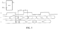
- FIG. 1 is a block circuit diagram and a sequence diagram of an existing latch.
- the latch includes an input end D, an output end Q, and a clock signal end CK.
- the operating principle of the latch is that when the clock signal CK is at a low level "0," data of the input end D is transmitted to the output end Q and latched by the latch until a next clock period.
- the data transmitted to the output end Q has delays relative to the clock signal CK and the input end D. For example, the delay relative to the clock signal CK is CK2Q, and the delay relative to the input end D is D2Q.
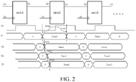
- FIG. 2 is a schematic diagram of a circuit structure and a sequence diagram of cascaded latches.
- a clock signal end CK of each level of the latches is connected to the same clock signal. Because when the clock signal is at a low level, data of an input end D of a former-level latch is directly transmitted to an output end Q, and a latter-level latch directly transmits new data to a next-level latch, causing data collusion. To resolve the data collusion, phases of the clock signals are staggered, and pulse widths of the clock signals are reduced.
- FIG. 3 is a schematic diagram of a circuit structure and a sequence diagram of cascaded latches using different clock signals in a first manner.
- a clock signal end CK of each level of the latches is connected to different clock signals.
- a clock signal end CK of a latch latch1 is connected to a clock signal CK1
- a clock signal end CK of a latch latch2 is connected to a clock signal CK2
- a clock signal end CK of a latch latch3 is connected to a clock signal CK3, and so on.
- the first three-level latches latch1, latch2, and latch3 are used as an example.
- FIG. 4 is a schematic diagram of a circuit structure and a sequence diagram of cascaded latches using different clock signals in another manner.
- a clock signal end CK of each of the latches is connected to different clock signals.
- a clock signal end CK of a latch latch1 is connected to a clock signal CK1
- a clock signal end CK of a latch latch2 is connected to a clock signal CK2
- a clock signal end CK of a latch latch3 is connected to a clock signal CK3, and so on. It can be learned from FIG.
- this application provides a clock generation circuit, a latch using same, and a computing device, which may effectively shape a clock pulse, reduce the use of a clock buffer, and improve the correctness and accuracy of data transmission and latching.
- this application provides a clock generation circuit, including: an input end, configured to input a pulse signal; a first output end, configured to output a first clock signal; a second output end, configured to output a second clock signal; and an input drive circuit, a latch circuit, an edge shaping circuit, a feedback delay unit, and an output drive circuit, where the input drive circuit, the latch circuit, the edge shaping circuit, the feedback delay unit, and the output drive circuit are sequentially connected between the input end and the first output end as well as the second output end in series.
- this application further provides a latch, including: a data input end, configured to input a data signal; a data output end, configured to output the data signal; a clock signal input end, configured to input a first clock signal; a plurality of levels of latch circuits, sequentially connected between the data input end and the data output end in series according to a first sequence; and a plurality of levels of clock generation circuits, sequentially connected in series according to a second sequence and electrically connected to the plurality of levels of latch circuits, where a direction of the first sequence is opposite to a direction of the second sequence, and the clock generation circuit is the clock generation circuit.
- this application further provides a computing device, including one or more latches.
- FIG. 5 is a schematic diagram of a circuit structure of a clock generation circuit, according to an embodiment of this application.
- a clock generation circuit 100 includes an input end CKI, a first output end CKO1, and a second output end CKO2.
- An input drive circuit 101, a latch circuit 102, an edge shaping circuit 103, a feedback delay unit 104, and an output drive circuit 105 are sequentially connected between the input end CKI and the first output end CKO1 as well as the second output end CKO2 in series.
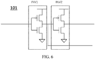
- FIG. 6 is a schematic diagram of a circuit structure of an input drive circuit, according to an embodiment of this application.
- the input drive circuit 101 is formed by two inverters INV1 and INV2 that are connected in series.
- Each of the inverters INV1 and INV2 includes an input end and an output end.
- the input end of the inverter INV1 is electrically connected to the input end CKI of the clock generation circuit 100 and is configured to provide an initial clock signal to the clock generation circuit 100.
- the output end of the inverter INV1 is electrically connected to the input end of the inverter INV2 and is electrically connected to the edge shaping circuit 103, and the output end of the inverter INV2 is electrically connected to the latch circuit 102.
- the input drive circuit 101 may alternatively be formed by a plurality of inverters connected in series, which is subject to enable two output signals electrically connected to the edge shaping circuit 103 and electrically connected to the latch circuit 102 to have inverted phases. This is not limited in this application.
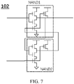
- FIG. 7 is a schematic diagram of a circuit structure of a latch circuit, according to an embodiment of this application.
- the latch circuit 102 is formed by two NAND gates NAND1 and NAND2 that are in cross-connection with each other.
- Each of the NAND gates NAND1 and NAND2 includes a first input end, a second input end, and an output end.
- the first input end of the NAND gate NAND1 is electrically connected to the output end of the NAND gate NAND2, the second input end of the NAND gate NAND1 is electrically connected to the feedback delay unit 104, the output end of the NAND gate NAND1 is electrically connected to the edge shaping circuit 103 and the second input end of the NAND gate NAND2, and the first input end of the NAND gate NAND2 is electrically connected to the output end of the inverter INV2.
- FIG. 8 is a schematic diagram of a circuit structure of an edge shaping circuit, according to an embodiment of this application.
- the edge shaping circuit includes PMOS transistors P1, P2, and P3 and NMOS transistors N1, N2, and N3.
- Each of the PMOS transistors or each of the NMOS transistors includes a first end, a second end, and a control end.
- the first ends of the PMOS transistors P1 and P2 are electrically connected to a power supply VDD
- the second ends of the PMOS transistors P1 and P2 are electrically connected to the first end of the PMOS transistor P3
- the second end of the PMOS transistor P3 is respectively electrically connected to the first ends of the NMOS transistors N1 and N2
- the second end of the NMOS transistor N2 is electrically connected to the first end of the NMOS transistor N3
- the second ends of the NMOS transistors N1 and N3 are electrically connected to a ground VSS
- the control ends of the PMOS transistor P1 and the NMOS transistor N2 are electrically connected to the output end of the inverter INV1
- the control ends of the PMOS transistor P3 and the NMOS transistor N1 are electrically connected to the output end of the NAND gate NAND1
- the control ends of the PMOS transistor P2 and the NMOS transistor N3 are electrically connected to the second end of the PMOS transistor P3 and are
- FIG. 9 is a schematic diagram of a circuit structure of a feedback delay unit, according to an embodiment of this application.
- the feedback delay circuit 104 is formed by a plurality of inverters connected in series.
- the feedback delay circuit 104 includes an input end and an output end.
- the input end of the feedback delay circuit 104 is electrically connected to the second end of the PMOS transistor P3 in the edge shaping circuit 103, and the output end of the feedback delay circuit 104 is electrically connected to the second input end of the NAND gate NAND1.
- the odd-numbered inverters form the feedback delay circuit 104, to output a signal inverted to that of the input end.
- a specific quantity depends on a duration required by delaying an input signal. This is not limited in this application.
- FIG. 10 is a schematic diagram of a circuit structure of an output drive circuit, according to an embodiment of this application.
- the output drive circuit 105 includes inverters INV3, INV4, and INV5.
- Each of the inverters INV3, INV4, and INV5 includes an input end and an output end.
- the input end of the inverter INV3 is electrically connected to the second end of the PMOS transistor P3 in the edge shaping circuit 103, the output end of the inverter INV3 is electrically connected to the first output end CKO1, the input end of the inverter INV4 is electrically connected to the input end of the inverter INV3 and the input ends of the inverters INV 3 and INV4 are jointly connected to the second end of the PMOS transistor P3 in the edge shaping circuit 103, the output end of the inverter INV4 is electrically connected to the input end of the inverter INV5, and the output end of the inverter INV5 is electrically connected to the second output end CKO2.
- the inverters INV3, INV4, and INV5 may alternatively be formed by connecting a plurality of inverters in series, which is subject to inversion of output signals of the first output end CKO1 and the second output end CKO2. This is not limited in this application.
- FIG. 11 is a schematic waveform diagram of a clock signal of a second output end of a clock generation circuit.
- the clock signals outputted by the first output end CKO1 and the second output end CKO2 of the clock generation circuit 100 are related to only a rising edge of the initial clock signal inputted by the input end CKI. Therefore, a pulse width of the clock signal outputted by the second output end CKO2 of the clock generation circuit 100 does not change regardless of whether a pulse width of the initial clock signal inputted by the input end CKI of the clock generation circuit 100 is wide or narrow.
- FIG. 12 is a sequence diagram of a latch unit under the control of a clock generation circuit, according to an embodiment of this application.
- correct transmission of data depends on a data setup time and a data hold time.
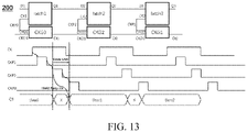
- FIG. 13 is a schematic diagram of a circuit structure and a sequence diagram of a latch, according to an embodiment of this application.
- the latch 200 includes cascaded latch circuits latch1, latch2, and latch3 and cascaded clock generation circuits CKG1, CKG2, and CKG3.
- a quantity of levels is three is used for description. In an actual application, there may be more levels. This is not limited in this application.
- a cascading sequence of the latch circuits latch1, latch2, and latch3 is a data transmission sequence, that is, from latch1 to latch2 to latch3, and a cascading sequence of the clock generation circuits CKG1, CKG2, and CKG3 is a clock signal transmission sequence, that is, from CKG1 to CKG2 to CKG3.
- the first-level clock generation circuit CKG1 is electrically connected to the third-level latch circuit latch3
- the second-level clock generation circuit CKG2 is electrically connected to the second-level latch circuit latch2
- the third-level clock generation circuit CKG3 is electrically connected to the first-level latch circuit latch1. That is, the cascading sequence of the latch circuits latch1, latch2, and latch3 is opposite to the cascading sequence of the clock generation circuits.
- the second output ends CKO2 of the clock generation circuits CKG1, CKG2, and CKG3 respectively provide clock signals CKP1, CKP2, and CKP3 to the latch circuits latch3, latch2, and latch1.
- the first output end CKO1 of the clock generation circuit CKG1 is electrically connected to the input end CKI of the clock generation circuit CKG2, and the first output end CKO1 of the clock generation circuit CKG2 is electrically connected to the input end CKI of the clock generation circuit CKG3.
- the clock signal outputted by the first output end CKO1 and the clock signal outputted by the second output end CKO2 have inverted phases.
- phases of the clock signals CKP1, CKP2, and CKP3 are completely staggered, and no phases overlap, which achieves higher efficiency compared with a case that the phases of the clock signals CKP1, CKP2, and CKP3 are staggered by connecting buffers, and more reliably ensures that the phases are completely staggered, and the buffers reduced.
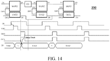
- FIG. 14 is a schematic diagram of a circuit structure and a sequence diagram of a latch, according to an embodiment of this application.
- a difference from the embodiment shown in FIG. 13 lies in that the first output end CKO1 of the clock generation circuit CKG1 is electrically connected to the input end CKI of the clock generation circuit CKG2 and the input end CKI of the clock generation circuit CKG3. Therefore, when there is a relatively large logic delay between two levels of adjacent latch circuits such as latch1 and latch2, for example, when an output end Q1 of latch1 and an input end D2 of latch2 are electrically connected to a delay circuit DC, a problem of clock setup of a critical timing path may be resolved, to improve the working efficiency of the latch.
- one level of latch circuit may correspond to one level of clock generation circuit, that is, one level of clock generation circuit provides a clock signal to one level of latch circuit.
- each level of latch circuit includes a plurality of latch units connected in series, a plurality of latch units connected in parallel, or a plurality of latch units in a combination of serial and parallel connections. That is, one level of clock generation circuit provides a clock signal to a plurality of latch units.
- each level of clock generation circuit may alternatively include a plurality of clock generation circuits, and one clock generation circuit corresponds to one latch unit. Therefore, the plurality of formed clock generation circuits are connected together to form a clock tree.
- a reverse clock tree is formed.
- functions of signal reestablishment and enhancement are implemented by using the second output end CKO2 of the clock generation circuit 100.
- the clock tree has a large fanout, that is, loading of the clock tree is large, the data transmission performance may be improved.
- the clock generation circuit provided by this application can generate a clock signal with the same pulse width regardless of a waveform of an initial clock signal of the clock generation circuit, and can effectively shape a pulse of the clock signal.
- the latch provided by this application can effectively implement complete staggering of phases of clock signals, reduce a quantity of used clock buffers, and improve the correctness and accuracy of data transmission and latching.
- This application further provides a computing device, including one or more latches, configured to store and transmit data.
- this application may further have a plurality of other embodiments.
- a person skilled in the art may make various corresponding changes and variations according to this application without departing from the spirit and essence of this application. However, such corresponding changes and variations shall fall within the protection scope of the claims appended to this application.
- the clock generation circuit, the latch using same, and the computing device provided in this application have the following beneficial effects.
- the clock generation circuit provided by this application may generate a clock signal with the same pulse width regardless of a waveform of an initial clock signal of the clock generation circuit, and may effectively shape a pulse of the clock signal.
- the latch may effectively implement complete staggering of phases between clock signals, reduce a quantity of used clock buffers, and improve the correctness and accuracy of data transmission and latching.
Landscapes
- Physics & Mathematics (AREA)
- Nonlinear Science (AREA)
- Engineering & Computer Science (AREA)
- Theoretical Computer Science (AREA)
- General Engineering & Computer Science (AREA)
- General Physics & Mathematics (AREA)
- Power Engineering (AREA)
- Computer Hardware Design (AREA)
- Computing Systems (AREA)
- Mathematical Physics (AREA)
- Manipulation Of Pulses (AREA)
Applications Claiming Priority (2)
| Application Number | Priority Date | Filing Date | Title |
|---|---|---|---|
| CN201911422474.4A CN113131902B (zh) | 2019-12-30 | 2019-12-30 | 时钟产生电路及应用其的锁存器和计算设备 |
| PCT/CN2020/098899 WO2021135102A1 (zh) | 2019-12-30 | 2020-06-29 | 时钟产生电路及应用其的锁存器和计算设备 |
Publications (2)
| Publication Number | Publication Date |
|---|---|
| EP4068630A1 true EP4068630A1 (de) | 2022-10-05 |
| EP4068630A4 EP4068630A4 (de) | 2023-01-25 |
Family
ID=76687073
Family Applications (1)
| Application Number | Title | Priority Date | Filing Date |
|---|---|---|---|
| EP20908872.3A Pending EP4068630A4 (de) | 2019-12-30 | 2020-06-29 | Takterzeugungsschaltung und verriegelung unter verwendung derselben sowie rechnervorrichtung |
Country Status (5)
| Country | Link |
|---|---|
| US (1) | US11799456B2 (de) |
| EP (1) | EP4068630A4 (de) |
| KR (1) | KR102674336B1 (de) |
| CN (1) | CN113131902B (de) |
| WO (1) | WO2021135102A1 (de) |
Families Citing this family (4)
| Publication number | Priority date | Publication date | Assignee | Title |
|---|---|---|---|---|
| CN113437961B (zh) * | 2021-08-26 | 2021-12-07 | 成都爱旗科技有限公司 | 一种锁存器及奇数分频电路 |
| CN114006605B (zh) * | 2021-12-31 | 2022-05-10 | 峰岹科技(深圳)股份有限公司 | 单边沿延时电路 |
| CN115756088A (zh) * | 2022-10-31 | 2023-03-07 | 杭州嘉楠耘智信息科技有限公司 | 时钟切换电路及应用其的时钟模块、芯片以及计算设备 |
| CN116072183B (zh) * | 2023-04-06 | 2023-08-22 | 长鑫存储技术有限公司 | 写入转换电路和存储器 |
Family Cites Families (19)
| Publication number | Priority date | Publication date | Assignee | Title |
|---|---|---|---|---|
| US4968906A (en) * | 1989-09-25 | 1990-11-06 | Ncr Corporation | Clock generating circuit for asynchronous pulses |
| US5453707A (en) * | 1993-01-13 | 1995-09-26 | Nec Corporation | Polyphase clock generation circuit |
| JP3732556B2 (ja) * | 1995-07-26 | 2006-01-05 | 東芝マイクロエレクトロニクス株式会社 | クロック供給回路 |
| US6049883A (en) | 1998-04-01 | 2000-04-11 | Tjandrasuwita; Ignatius B. | Data path clock skew management in a dynamic power management environment |
| US6169704B1 (en) * | 1998-05-20 | 2001-01-02 | Micron Technology, Inc. | Apparatus and method for generating a clock within a semiconductor device and devices and systems including same |
| US6831493B2 (en) * | 1998-10-30 | 2004-12-14 | Mosaid Technologies Incorporated | Duty cycle regulator |
| US6571948B2 (en) | 2001-06-28 | 2003-06-03 | Bellsouth Intellectual Property Corporation | Keyboard lock box |
| KR100445062B1 (ko) * | 2001-11-02 | 2004-08-21 | 주식회사 하이닉스반도체 | 반도체메모리장치의 클럭발생회로 |
| US6809983B2 (en) * | 2003-03-25 | 2004-10-26 | Lsi Logic Corporation | Clock generator for pseudo dual port memory |
| US7319355B2 (en) * | 2006-01-03 | 2008-01-15 | Taiwan Semiconductor Manufacturing Co., Ltd. | Pulse generator |
| KR20080027048A (ko) * | 2006-09-22 | 2008-03-26 | 삼성전자주식회사 | 고속 저전력으로 동작하기 위한 듀얼 엣지 트리거 클록게이트 로직 및 그 방법 |
| KR100853649B1 (ko) * | 2007-04-02 | 2008-08-25 | 삼성전자주식회사 | 레벨 컨버팅 기능을 포함하는 클럭-게이티드 래치 |
| CN102075167B (zh) * | 2010-11-22 | 2014-03-12 | 西安电子科技大学 | 时钟调整电路和时钟电路的调整方法 |
| CN102185590A (zh) * | 2011-03-24 | 2011-09-14 | 无锡思泰迪半导体有限公司 | 用于高速系统的两相不交叠时钟产生电路 |
| US8949652B2 (en) | 2011-11-03 | 2015-02-03 | Nvidia Corporation | Glitchless programmable clock shaper |
| US8952740B2 (en) * | 2013-02-01 | 2015-02-10 | Industrial Technology Research Institute | Pulsed latching apparatus and method for generating pulse signal of pulsed latch thereof |
| CN103837243B (zh) | 2014-03-27 | 2016-08-24 | 卓捷创芯科技(深圳)有限公司 | 时间域集成温度传感器 |
| US9627012B1 (en) * | 2016-06-29 | 2017-04-18 | International Business Machines Corporation | Shift register with opposite shift data and shift clock directions |
| JP2019008859A (ja) | 2017-06-28 | 2019-01-17 | 東芝メモリ株式会社 | 半導体装置 |
-
2019
- 2019-12-30 CN CN201911422474.4A patent/CN113131902B/zh active Active
-
2020
- 2020-06-29 EP EP20908872.3A patent/EP4068630A4/de active Pending
- 2020-06-29 KR KR1020227025861A patent/KR102674336B1/ko active Active
- 2020-06-29 WO PCT/CN2020/098899 patent/WO2021135102A1/zh not_active Ceased
-
2022
- 2022-06-30 US US17/855,281 patent/US11799456B2/en active Active
Also Published As
| Publication number | Publication date |
|---|---|
| WO2021135102A1 (zh) | 2021-07-08 |
| KR102674336B1 (ko) | 2024-06-11 |
| US20220337229A1 (en) | 2022-10-20 |
| KR20220120652A (ko) | 2022-08-30 |
| CN113131902A (zh) | 2021-07-16 |
| US11799456B2 (en) | 2023-10-24 |
| CN113131902B (zh) | 2023-04-11 |
| EP4068630A4 (de) | 2023-01-25 |
Similar Documents
| Publication | Publication Date | Title |
|---|---|---|
| US11799456B2 (en) | Clock generation circuit and latch using same, and computing device | |
| CN104269132B (zh) | 一种移位寄存单元、显示面板和显示装置 | |
| CN104361853B (zh) | 移位寄存器单元、移位寄存器、栅极驱动电路和显示装置 | |
| US9799296B2 (en) | CMOS GOA circuit | |
| US10878857B2 (en) | Dynamic data storage element, and integrated circuit having the same | |
| TWI488163B (zh) | 移位暫存器、使用該移位暫存器之閘極驅動電路與顯示裝置 | |
| US20150303925A1 (en) | Output Buffer, Gate Electrode Driving Circuit and Method for Controlling the Same | |
| US20080080262A1 (en) | Data alignment circuit and data alignment method for semiconductor memory device | |
| CN104933982B (zh) | 移位寄存单元、移位寄存器、栅极驱动电路和显示装置 | |
| CN104658508B (zh) | 一种移位寄存器单元、栅极驱动电路及显示装置 | |
| CN107767809A (zh) | 栅极驱动单元、驱动方法和栅极驱动电路 | |
| US7180351B2 (en) | Hybrid latch flip-flop | |
| CN102375472A (zh) | 用于脉冲锁存器的时钟树 | |
| CN106057117A (zh) | 移位寄存单元、移位寄存器及显示面板 | |
| TWI515707B (zh) | 影像顯示系統、移位暫存器與移位暫存器控制方法 | |
| CN100472664C (zh) | 移位寄存器以及显示装置 | |
| CN110688024B (zh) | 移位寄存器及具有移位寄存器的触控显示装置 | |
| US20090185437A1 (en) | Clock-based data storage device, dual pulse generation device, and data storage device | |
| CN107491208B (zh) | 触控驱动单元、触控驱动电路和显示装置 | |
| HK40075488A (en) | Clock generation circuit and latch using same, and computing device | |
| CN114203094A (zh) | Goa电路及显示面板 | |
| TW201602993A (zh) | 驅動電路和顯示裝置 | |
| US20040160257A1 (en) | Latch-based pulse generator | |
| EA045538B1 (ru) | Схема генерации тактовых импульсов и триггер, использующий ее, и вычислительное устройство | |
| CN101295970B (zh) | 触发器与移位寄存器 |
Legal Events
| Date | Code | Title | Description |
|---|---|---|---|
| STAA | Information on the status of an ep patent application or granted ep patent |
Free format text: STATUS: THE INTERNATIONAL PUBLICATION HAS BEEN MADE |
|
| PUAI | Public reference made under article 153(3) epc to a published international application that has entered the european phase |
Free format text: ORIGINAL CODE: 0009012 |
|
| STAA | Information on the status of an ep patent application or granted ep patent |
Free format text: STATUS: REQUEST FOR EXAMINATION WAS MADE |
|
| 17P | Request for examination filed |
Effective date: 20220629 |
|
| AK | Designated contracting states |
Kind code of ref document: A1 Designated state(s): AL AT BE BG CH CY CZ DE DK EE ES FI FR GB GR HR HU IE IS IT LI LT LU LV MC MK MT NL NO PL PT RO RS SE SI SK SM TR |
|
| REG | Reference to a national code |
Ref country code: HK Ref legal event code: DE Ref document number: 40075488 Country of ref document: HK |
|
| A4 | Supplementary search report drawn up and despatched |
Effective date: 20230103 |
|
| RIC1 | Information provided on ipc code assigned before grant |
Ipc: H03K 5/133 20140101ALI20221221BHEP Ipc: H03K 3/356 20060101ALI20221221BHEP Ipc: H03K 3/012 20060101ALI20221221BHEP Ipc: H03K 5/06 20060101ALI20221221BHEP Ipc: H03K 3/017 20060101AFI20221221BHEP |
|
| DAV | Request for validation of the european patent (deleted) | ||
| DAX | Request for extension of the european patent (deleted) | ||
| P01 | Opt-out of the competence of the unified patent court (upc) registered |
Effective date: 20230529 |
|
| STAA | Information on the status of an ep patent application or granted ep patent |
Free format text: STATUS: EXAMINATION IS IN PROGRESS |
|
| 17Q | First examination report despatched |
Effective date: 20250124 |