EP4068800A1 - Module de détection de pression et dispositif électronique - Google Patents
Module de détection de pression et dispositif électronique Download PDFInfo
- Publication number
- EP4068800A1 EP4068800A1 EP21769869.5A EP21769869A EP4068800A1 EP 4068800 A1 EP4068800 A1 EP 4068800A1 EP 21769869 A EP21769869 A EP 21769869A EP 4068800 A1 EP4068800 A1 EP 4068800A1
- Authority
- EP
- European Patent Office
- Prior art keywords
- circuit board
- pressure detection
- detection module
- electrode
- module according
- Prior art date
- Legal status (The legal status is an assumption and is not a legal conclusion. Google has not performed a legal analysis and makes no representation as to the accuracy of the status listed.)
- Ceased
Links
Images



Classifications
-
- G—PHYSICS
- G06—COMPUTING OR CALCULATING; COUNTING
- G06F—ELECTRIC DIGITAL DATA PROCESSING
- G06F3/00—Input arrangements for transferring data to be processed into a form capable of being handled by the computer; Output arrangements for transferring data from processing unit to output unit, e.g. interface arrangements
- G06F3/01—Input arrangements or combined input and output arrangements for interaction between user and computer
- G06F3/03—Arrangements for converting the position or the displacement of a member into a coded form
- G06F3/041—Digitisers, e.g. for touch screens or touch pads, characterised by the transducing means
- G06F3/0414—Digitisers, e.g. for touch screens or touch pads, characterised by the transducing means using force sensing means to determine a position
-
- G—PHYSICS
- G01—MEASURING; TESTING
- G01L—MEASURING FORCE, STRESS, TORQUE, WORK, MECHANICAL POWER, MECHANICAL EFFICIENCY, OR FLUID PRESSURE
- G01L1/00—Measuring force or stress, in general
- G01L1/14—Measuring force or stress, in general by measuring variations in capacitance or inductance of electrical elements, e.g. by measuring variations of frequency of electrical oscillators
- G01L1/142—Measuring force or stress, in general by measuring variations in capacitance or inductance of electrical elements, e.g. by measuring variations of frequency of electrical oscillators using capacitors
- G01L1/144—Measuring force or stress, in general by measuring variations in capacitance or inductance of electrical elements, e.g. by measuring variations of frequency of electrical oscillators using capacitors with associated circuitry
-
- G—PHYSICS
- G01—MEASURING; TESTING
- G01D—MEASURING NOT SPECIALLY ADAPTED FOR A SPECIFIC VARIABLE; ARRANGEMENTS FOR MEASURING TWO OR MORE VARIABLES NOT COVERED IN A SINGLE OTHER SUBCLASS; TARIFF METERING APPARATUS; MEASURING OR TESTING NOT OTHERWISE PROVIDED FOR
- G01D5/00—Mechanical means for transferring the output of a sensing member; Means for converting the output of a sensing member to another variable where the form or nature of the sensing member does not constrain the means for converting; Transducers not specially adapted for a specific variable
- G01D5/12—Mechanical means for transferring the output of a sensing member; Means for converting the output of a sensing member to another variable where the form or nature of the sensing member does not constrain the means for converting; Transducers not specially adapted for a specific variable using electric or magnetic means
- G01D5/14—Mechanical means for transferring the output of a sensing member; Means for converting the output of a sensing member to another variable where the form or nature of the sensing member does not constrain the means for converting; Transducers not specially adapted for a specific variable using electric or magnetic means influencing the magnitude of a current or voltage
- G01D5/24—Mechanical means for transferring the output of a sensing member; Means for converting the output of a sensing member to another variable where the form or nature of the sensing member does not constrain the means for converting; Transducers not specially adapted for a specific variable using electric or magnetic means influencing the magnitude of a current or voltage by varying capacitance
-
- G—PHYSICS
- G01—MEASURING; TESTING
- G01L—MEASURING FORCE, STRESS, TORQUE, WORK, MECHANICAL POWER, MECHANICAL EFFICIENCY, OR FLUID PRESSURE
- G01L1/00—Measuring force or stress, in general
- G01L1/14—Measuring force or stress, in general by measuring variations in capacitance or inductance of electrical elements, e.g. by measuring variations of frequency of electrical oscillators
-
- G—PHYSICS
- G06—COMPUTING OR CALCULATING; COUNTING
- G06F—ELECTRIC DIGITAL DATA PROCESSING
- G06F3/00—Input arrangements for transferring data to be processed into a form capable of being handled by the computer; Output arrangements for transferring data from processing unit to output unit, e.g. interface arrangements
- G06F3/01—Input arrangements or combined input and output arrangements for interaction between user and computer
- G06F3/03—Arrangements for converting the position or the displacement of a member into a coded form
- G06F3/041—Digitisers, e.g. for touch screens or touch pads, characterised by the transducing means
- G06F3/044—Digitisers, e.g. for touch screens or touch pads, characterised by the transducing means by capacitive means
-
- H—ELECTRICITY
- H03—ELECTRONIC CIRCUITRY
- H03K—PULSE TECHNIQUE
- H03K17/00—Electronic switching or gating, i.e. not by contact-making and –breaking
- H03K17/94—Electronic switching or gating, i.e. not by contact-making and –breaking characterised by the way in which the control signals are generated
- H03K17/96—Touch switches
- H03K17/962—Capacitive touch switches
-
- H—ELECTRICITY
- H03—ELECTRONIC CIRCUITRY
- H03K—PULSE TECHNIQUE
- H03K17/00—Electronic switching or gating, i.e. not by contact-making and –breaking
- H03K17/94—Electronic switching or gating, i.e. not by contact-making and –breaking characterised by the way in which the control signals are generated
- H03K17/965—Switches controlled by moving an element forming part of the switch
- H03K17/975—Switches controlled by moving an element forming part of the switch using a capacitive movable element
-
- H—ELECTRICITY
- H03—ELECTRONIC CIRCUITRY
- H03K—PULSE TECHNIQUE
- H03K2217/00—Indexing scheme related to electronic switching or gating, i.e. not by contact-making or -breaking covered by H03K17/00
- H03K2217/94—Indexing scheme related to electronic switching or gating, i.e. not by contact-making or -breaking covered by H03K17/00 characterised by the way in which the control signal is generated
- H03K2217/96—Touch switches
- H03K2217/9607—Capacitive touch switches
- H03K2217/960755—Constructional details of capacitive touch and proximity switches
-
- H—ELECTRICITY
- H03—ELECTRONIC CIRCUITRY
- H03K—PULSE TECHNIQUE
- H03K2217/00—Indexing scheme related to electronic switching or gating, i.e. not by contact-making or -breaking covered by H03K17/00
- H03K2217/94—Indexing scheme related to electronic switching or gating, i.e. not by contact-making or -breaking covered by H03K17/00 characterised by the way in which the control signal is generated
- H03K2217/965—Switches controlled by moving an element forming part of the switch
- H03K2217/9651—Switches controlled by moving an element forming part of the switch the moving element acting on a force, e.g. pressure sensitive element
Definitions
- the present disclosure relates to the field of electronic technology, and in particular to a pressure detection module and an electronic device.
- Electronic devices such as earphones may detect whether they are pressed through pressure detection modules installed inside, so as to perform operation control corresponding to the pressing.
- a pressure detection module installed in an earphone determines whether the earphone is pressed, thereby controlling the playback of music in the earphone.
- a pressure detection module is usually disposed in a narrow space of an electronic device, and how to reduce an internal space of the electronic device occupied by the pressure detection module, especially a thickness of the electronic device, has become an urgent technical problem to be solved.
- one of the technical problems solved by embodiments of the present disclosure is to provide a pressure detection module and an electronic device to partially or completely solve the technical problems existing in the prior art.
- an embodiment of the present disclosure provides a pressure detection module.
- the pressure detection module is disposed on an inner surface of a housing of an electronic device, and the pressure detection module includes: a first electrode, a second electrode, a first circuit board, a second circuit board, and at least two solder fixing parts for fixing the first circuit board and the second circuit board; a first surface of the first circuit board is fixed to an inner surface of a force input area of the housing, a second surface of the first circuit board is fixed to a first surface of the first electrode, and a first surface of the second circuit board is fixed to a second surface of the second electrode; two end sides of the second surface of the first circuit board and two end sides of the first surface of the second circuit board are disposed opposed to each other through the at least two solder fixing parts, and a compressible insulating layer is provided between a second surface of the first electrode and a first surface of the second electrode so that the first electrode and the second electrode form a capacitor; and the force input area of the housing drives the first electrode to move
- an embodiment of the present disclosure provides an electronic device, having at least one the above pressure detection module inside a housing of the electronic device.
- the pressure detection module and the electronic device provided by the embodiments of the present disclosure, since the first surface of the first electrode included in the pressure detection module is fixed to the inner surface of the force input area of the housing, the second surface of the first circuit board is fixed to the first surface of the first electrode, the first surface of the second circuit board is fixed to the second surface of the second electrode, the two end sides of the second surface of the first circuit board and the two end sides of the first surface of the second circuit board are disposed opposed to each other through the solder fixing parts, and the compressible insulating layer is provided between the second surface of the first electrode and the first surface of the second electrode so that the first electrode and the second electrode form the capacitor.
- the pressure detection module according to an embodiment of the present disclosure only needs to be installed on the inner surface of the force input area of the housing to achieve pressure detection, no bracket is required, and the thickness of the pressure detection module is small, thereby facilitating installation of other elements inside the electronic device.
- the relative arrangement of the first electrode and the second electrode does not need to occupy an area of the two, which improves an accuracy of sensing the external pressure through the first electrode and the second electrode, and provides a better adhesion effect of relatively fixedly disposing the first circuit board and the second circuit board.
- embodiments of the present disclosure provide a pressure detection module and an electronic device.
- a specific implementation of the embodiments of the present utility model will be further described below in conjunction with the accompanying drawings of the embodiments of the present utility model.
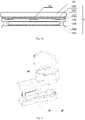
- FIG. 1 is a structural diagram of a pressure detection module provided by Embodiment 1 of the present disclosure.
- a pressure detection module 10 is disposed on an inner surface of a housing 20 of an electronic device, and the pressure detection module 10 includes: a first electrode 101, a second electrode 102, a first circuit board 103, a second circuit board 104, and at least two solder fixing parts 105 for fixing the first circuit board and the second circuit board.
- a first surface of the first circuit board 103 is fixed to an inner surface of a force input area of the housing 20, a second surface of the first circuit board 103 is fixed to a first surface of the first electrode 101, and a first surface of the second circuit board 104 is fixed to a second surface of the second electrode 102.
- Two end sides of the second surface of the first circuit board 103 and two end sides of the first surface of the second circuit 104 board are disposed opposed to each other through the solder fixing parts 105, and a compressible insulating layer is provided between a second surface of the first electrode 101 and a first surface of the second electrode 102 so that the first electrode 101 and the second electrode 102 form a capacitor.
- the force input area of the housing 20 drives the first electrode 101 to move towards the second electrode 102 based on received external pressure, so that the capacitance between the first electrode 101 and the second electrode 102 changes to determine a pressure detection result on the external pressure.
- the force input area of the housing 20 is an area of any shape.
- the force input area may use any marking to indicate that a user may apply pressure in this area.
- a position of a center of the force input area corresponds to a position of a center of the first electrode, so that the user drives the first electrode to move towards the second electrode through the external pressure applied by the force input area.
- the compressible insulating layer is air.
- the embodiment of the present disclosure is based on the above arrangement and the compressible insulating layer is air, so as to reduce an assembly difficulty and reduce production costs.
- the center of the force input area of the housing 20 When the force input area of the housing 20 receives an external force and deforms, the center of the force input area deforms the most, and the center of the force input area corresponds to the center of the first electrode 101.
- the force input area of the housing 20 receives the external force, the first electrode 101 fixed to the housing 20 deforms with the deformation of the housing 20, the deformation of the first electrode 101 is consistent with that of the housing 20, and the second electrode 102 is fixed to the second circuit board 104, the two end sides of the second circuit board 104 are fixedly disposed to the first circuit board 103 through the solder fixing parts, and there is the compressible insulating layer between the first electrode 101 and the second electrode 102, therefore, the second electrode 102 deforms following deformation of the second circuit board 104.
- a deformation displacement in a pressing center is larger than that of the two ends, that is, a deformation displacement of the first electrode 101 is larger than that of the second electrode 102, a distance between the first electrode 101 and the second electrode 102 changes, resulting in a change in the capacitance. Based on the change in the capacitance, the pressure detection result on the external pressure may be determined.
- the two end sides of the second surface of the first circuit board 103 refer to portions not fixed to the first electrode and located on both sides of the first electrode; the two end sides of the first surface of the second circuit board 104 refer to portions not fixed to the second electrode and located on both sides of the second electrode.
- the pressure detection module according to the embodiment of the present disclosure only needs to be installed on the inner surface of the force input area of the housing to achieve pressure detection. There is no need for a bracket and a thickness of the pressure detection module is reduced, thereby facilitating installation of other elements inside the electronic device, and facilitating reducing interference effects between the pressure detection module and other electronic components in a miniaturized electronic device.
- the two end sides of the second surface of the first circuit board and the two end sides of the first surface of the second circuit board in the embodiment of the present disclosure are disposed opposed to each other through the solder fixing parts, so that the first electrode on the second surface of the first circuit board and the second electrode on the first surface of the second circuit board are disposed opposed to each other, do not occupy an area of the first electrode and the second electrode, and only occupy a small area of the first circuit board and the second circuit board, which is beneficial to provide a larger first electrode and second electrode on the pressure detection module, further improve an accuracy of sensing the external pressure through the first electrode and the second electrode, making it easier to assemble elements and saving costs.
- the embodiment of the present disclosure provides a better adhesion effect of relatively fixedly disposing the first circuit board and the second circuit board through the solder fixing parts, so that when the electronic device is not subjected to external pressure, a relative position of the first electrode on the first circuit board and the second electrode on the second circuit board is more stable and reliable, which is also beneficial for the pressure detection module to be installed in the housing of the electronic device as a whole.
- the solder fixing parts do not need to be glued, the solder fixing parts are not easy to age, and a production process of the solder fixing parts adopts a surface mount technology, which is convenient for automation and may save manpower.
- the solder fixing parts are more stable and reliable than glue connection, which is more conducive to improving the accuracy and consistency of pressure detection.
- an adhesion effect of the solder fixing parts is better than an adhesion effect of glue or a double-sided tape, so that when the same adhesion effect is required, smaller solder fixing parts may be used, so as to reduce space occupied by the solder fixing parts and increase the area of the first electrode and the second electrode, to improve a signal volume and the accuracy of pressure detection.
- the solder fixing parts 105 are provided on edge sides of the first circuit board 103 and the second circuit board 104 away from the first electrode 101 and the second electrode 102.
- the embodiment of the present disclosure is based on the above arrangement, and providing the solder fixing parts 105 on the edge sides away from the first electrode 101 and the second electrode 102 can further avoid influence of the solder fixing parts 105 on the first electrode 101 and the second electrode 102, and improve the accuracy of sensing the external pressure through the first electrode 102 and the second electrode 103.
- the distance between the first electrode and the second electrode is very short and the area of the first electrode and the second electrode is very small, which may cause a capacitance signal volume to be small, so that a backend detection circuit cannot detect a capacitance signal or a detected signal is very weak. Therefore, the present embodiment may make the first electrode and the second electrode in the pressure detection module in a small headphone space be set larger, thereby increasing the signal volume of the capacitance signal between the first electrode and the second electrode, in order to help improve the accuracy of pressure detection.
- positions of the solder fixing parts 105 on one end side of the first circuit board 103 and the second circuit board 104 are disposed to be symmetrical with positions of the solder fixing parts 105 on the other end side of the first circuit board 103 and the second circuit board 104; and/or, the number of the solder fixing parts 105 located on one end side of the first circuit board and the second circuit board is the same as the number of the solder fixing parts located on the other end side of the first circuit board 103 and the second circuit board 104.
- the embodiment of the present disclosure is based on the above arrangement and the positions of the solder fixing parts 105 are symmetrically disposed or the number is symmetrically set, which can provide a better adhesion effect of relatively fixedly disposing the first circuit board 103 and the second circuit board 104.
- a height of the solder fixing parts 105 is greater than or equal to 0.05 mm to less than or equal to 0.15 mm.
- the embodiment of the present disclosure is based on the above arrangement and the height of the solder fixing parts 105, which may ensure that a detected pressure signal reaches a certain volume of signal, so as to avoid undetected signals or weak detected signals that affect the accuracy of pressure detection. It may also reduce a volume and thickness of the pressure detection module, simplify a manufacturing process and improve a consistency and yield of the product, which is more conducive to miniaturization of the electronic device.
- pads of the solder fixing parts 105 in contact with the first circuit board 103 and the second circuit board 104 are in a rectangle shape with a single side greater than or equal to 0.3 mm.
- the embodiment of the present disclosure is based on the above arrangement and an area of the pads can achieve a good fixing effect between the first circuit board 103 and the second circuit board 104.
- the number of the solder fixing parts 105 on each end side is two or three, to ensure the good fixing effect between the first circuit board 103 and the second circuit board 104 while avoiding occupying too much area of the first circuit board 103 and the second circuit board 104.
- the second electrode 102 is electrically connected to a chip through the solder fixing parts 105, so that the solder fixing parts 105 may achieve adhesion and fixing while conducting electrical connection, in order to further save an area occupied by the second circuit board 104.
- wiring may be reduced, thereby reducing interference of wiring to the electronic device.
- the pressure detection module 10 further includes: a first adhesion layer 106.
- the first surface of the first circuit board 103 is fixed to the inner surface of the force input area of the housing 20 through the first adhesion layer 106.
- the first circuit board is adhered to the inner surface of the force input area of the housing 20 through the first adhesion layer, which makes installation easier.
- the first adhesion layer 106 is a layered structure with adhesion on both upper and lower surfaces thereof, so that adhesion between the first circuit board 103 and the inner surface of the force input area of the housing 20 can be easily achieved.
- the first adhesion layer 106 is a double-sided tape.
- a thickness of the double-sided tape is less than or equal to 0.15 mm.
- the thickness of the double-sided tape is 0.1 mm.
- the first circuit board in order that the first electrode is better adhered to the second surface of the first circuit board, the first circuit board may be a rigid printed circuit board; and/or in order that the second electrode is better adhered to the first surface of the second circuit board, the second circuit board may be a rigid printed circuit board.
- the pressure detection module further includes: a first stiffener 107, and the first stiffener 107 is fixed on the first surface of the first circuit board 103.
- the first stiffener 107 is provided on the first surface of the first circuit board 103, so that the pressure detection module may be disposed as a whole inside the housing of the electronic device, so that the pressure detection module provided by the present embodiment may be suitable for electronic devices with non-detachable housings, for example, suitable for a structure in which a pull rod of the earphone is a cylindrical whole, thereby improving convenience of installing the pressure detection module on the electronic device.
- a supporting function of the first stiffener also enables the first circuit board to have better flatness.
- the housing of the pull rod may be disassembled, that is, the housing of the pull rod may be divided into an upper housing and a lower housing, the pressure detection module is first disposed inside the lower housing of the pull rod, and then the upper housing of the pull rod is buckled on the lower housing.
- the pressure detection module with the first stiffener because the first stiffener increases strength, there is no need to disassemble the housing of the pull rod, and the whole pressure detection module may be directly disposed inside the cylindrical housing.
- the first stiffener is made of an insulating material, so that the pressure detection module provided in the embodiment of the present disclosure may achieve pressure detection and touch detection at the same time.
- the pressure detection module 10 further includes: a first stiffened laminated layer 108, and the first stiffener 107 is fixed on the first surface of the first circuit board 103 through the first stiffened laminated layer 108.
- the first stiffener is fixed on the first surface of the first circuit board through the first stiffened laminated layer, which improves fitness and flatness between the first stiffener and the first surface of the first circuit board.
- a total thickness of the first stiffener 107 and the first stiffened laminated layer 108 is less than or equal to 0.2 mm.
- the total thickness of the first stiffener 107 and the first stiffened laminated layer 108 is 0.2 mm.
- the pressure detection module 10 further includes: a second stiffener 109, and the second stiffener 109 is fixed on a second surface of the second circuit board 104.
- the second stiffener is provided on the second surface of the second circuit board, so that the second circuit board is more closely adhered to the second surface of the second electrode.
- a supporting function of the second stiffener also enables the second electrode to have better flatness.
- the second stiffener 109 is a steel plate, which can provide better support, better flatness, and simple and convenient manufacturing process.
- the pressure detection module further includes: a second stiffened laminated layer 110, and the second stiffener 109 is fixed on the second surface of the second circuit board 104 through the second stiffened laminated layer 110.
- the second stiffener is fixed on the second surface of the second circuit board through the second stiffened laminated layer, which improves fitness and flatness between the second stiffener and the second circuit board.
- a total thickness of the second stiffener 109 and the second stiffened laminated layer 110 is less than or equal to 0.15 mm.
- the total thickness of the second stiffener 109 and the second stiffened laminated layer 110 is 0.15 mm.
- At least one touch sensor 30 is provided on the first surface of the first circuit board 103.
- At least one touch sensor 30 is provided on the first surface of the first circuit board 103, and the first stiffener 107 is an insulated stiffener, so that the touch sensor can detect the user's touch.
- the embodiment of the present disclosure installs both the touch sensor and the first electrode on the first circuit board, so that the first electrode for detecting pressure and the touch sensor for detecting touch are both located on the same side of the housing and at the same position on the same side (that is, the housing where the force input area is located). Further, the first circuit board may simultaneously sense the user's touch and pressure applied by the user through the force input area of the housing.
- the structure of the first circuit board is simple, an installation process thereof may also be simplified, and the simple structure and the simplified process may further improve the consistency of the product and improve the yield of the product.
- the embodiment of the present disclosure may further save the internal space of the electronic device, and facilitate the installation of other internal elements.
- a length of the first circuit board is greater than or equal to 5 mm, so that the at least one touch sensor on the first circuit board may better realize touch sensing.
- an embodiment of the present disclosure provides an electronic device, and the electronic device has the pressure detection module in any one of the above embodiments inside a housing thereof.
- a thickness of the housing is less than or equal to 1 mm. Therefore, the present embodiment can also reduce a weight of the housing as much as possible while meeting the strength of the housing.
- the electronic device includes: a wireless Bluetooth earphone, a smart glass, etc.
- the pressure detection module according to the embodiment of the present disclosure is installed in a pull rod of the wireless Bluetooth earphone or smart glass, and the pull rod is a rod-shaped part connected with an earpiece or a lens.
- the electronic device is an earphone or a smart glass
- the pressure detection module is detachably disposed inside a housing of a pull rod of the earphone or smart glass.
- the pressure detection module 10 is disposed in a pull rod 40.
- the pressure detection module is detachably disposed in the pull rod 40.
- the pressure detection module is detachably disposed in a middle section of the pull rod 40, facilitating replacement and maintenance of the pressure detection module.
- the pressure detection module 10 with the first stiffener is suitable for being non-detachably installed inside the housing of the pull rod 40 of the wireless Bluetooth earphone as a whole, without disassembling the pull rod 40, which is convenient for installation, replacement and maintenance.
- the pressure detection module according to the embodiment of the present disclosure only needs to be installed on the inner surface of the force input area of the housing to achieve pressure detection. There is no need for a bracket and the thickness of the pressure detection module is reduced, thereby facilitating the installation of other elements inside the electronic device, and facilitating reducing interference effects between the pressure detection module and other electronic components in a miniaturized electronic device.
- the two end sides of the second surface of the first circuit board and the two end sides of the first surface of the second circuit board in the embodiment of the present disclosure are disposed opposed to each other through the solder fixing parts, so that the first electrode on the second surface of the first circuit board and the second electrode on the first surface of the second circuit board are disposed opposed to each other, do not occupy an area of the first electrode and the second electrode, and only occupy a small area of the first circuit board and the second circuit board, thereby improving the accuracy of sensing the external pressure through the first electrode and the second electrode, making it easier to assemble elements and saving costs.
- the embodiment of the present disclosure provides a better adhesion effect of relatively fixedly disposing the first circuit board and the second circuit board, the solder fixing parts do not need to be glued, the solder fixing parts are not easy to age, and the production process adopts the surface mount technology, which is convenient for automation and may save manpower.
Landscapes
- Engineering & Computer Science (AREA)
- Physics & Mathematics (AREA)
- General Physics & Mathematics (AREA)
- General Engineering & Computer Science (AREA)
- Theoretical Computer Science (AREA)
- Power Engineering (AREA)
- Human Computer Interaction (AREA)
- Measuring Fluid Pressure (AREA)
- Force Measurement Appropriate To Specific Purposes (AREA)
Applications Claiming Priority (2)
| Application Number | Priority Date | Filing Date | Title |
|---|---|---|---|
| PCT/CN2021/076377 WO2022170527A1 (fr) | 2021-02-09 | 2021-02-09 | Module de détection de pression et dispositif électronique |
| PCT/CN2021/094710 WO2022170688A1 (fr) | 2021-02-09 | 2021-05-19 | Module de détection de pression et dispositif électronique |
Publications (2)
| Publication Number | Publication Date |
|---|---|
| EP4068800A1 true EP4068800A1 (fr) | 2022-10-05 |
| EP4068800A4 EP4068800A4 (fr) | 2022-10-05 |
Family
ID=81060217
Family Applications (1)
| Application Number | Title | Priority Date | Filing Date |
|---|---|---|---|
| EP21769869.5A Ceased EP4068800A4 (fr) | 2021-02-09 | 2021-05-19 | Module de détection de pression et dispositif électronique |
Country Status (5)
| Country | Link |
|---|---|
| US (1) | US12085459B2 (fr) |
| EP (1) | EP4068800A4 (fr) |
| KR (1) | KR20220116382A (fr) |
| CN (1) | CN216284032U (fr) |
| WO (1) | WO2022170749A1 (fr) |
Cited By (1)
| Publication number | Priority date | Publication date | Assignee | Title |
|---|---|---|---|---|
| EP4369607A4 (fr) * | 2021-07-08 | 2024-11-06 | Vivo Mobile Communication Co., Ltd. | Touche sensible à la pression et dispositif électronique |
Families Citing this family (2)
| Publication number | Priority date | Publication date | Assignee | Title |
|---|---|---|---|---|
| CN115243448B (zh) * | 2022-07-22 | 2025-09-05 | 深圳市景旺电子股份有限公司 | 压力感应模组及其制作方法、电子装置 |
| WO2026000290A1 (fr) * | 2024-06-27 | 2026-01-02 | 深圳市汇顶科技股份有限公司 | Appareil de détection de pression et dispositif électronique |
Family Cites Families (31)
| Publication number | Priority date | Publication date | Assignee | Title |
|---|---|---|---|---|
| US4587378A (en) | 1984-07-30 | 1986-05-06 | Koala Technologies Corporation | Two-layer touch tablet |
| SE443057B (sv) | 1984-08-09 | 1986-02-10 | Tecator Ab | Anordning och sett for registrering av en utmed en strecka gjord analog legesangivelse som en digital signal |
| US20060001655A1 (en) | 2004-07-01 | 2006-01-05 | Koji Tanabe | Light-transmitting touch panel and detection device |
| CN101490642A (zh) | 2006-07-18 | 2009-07-22 | Iee国际电子工程股份公司 | 输入设备 |
| US8063886B2 (en) | 2006-07-18 | 2011-11-22 | Iee International Electronics & Engineering S.A. | Data input device |
| US20120228109A1 (en) * | 2011-03-08 | 2012-09-13 | Ibiden Co., Ltd. | Sensor, keyboard and method for manufacturing sensor |
| US20130001550A1 (en) | 2011-06-29 | 2013-01-03 | Invensense, Inc. | Hermetically sealed mems device with a portion exposed to the environment with vertically integrated electronics |
| US20130018489A1 (en) * | 2011-07-14 | 2013-01-17 | Grunthaner Martin Paul | Combined force and proximity sensing |
| US9490804B2 (en) * | 2011-09-28 | 2016-11-08 | Cypress Semiconductor Corporation | Capacitance sensing circuits, methods and systems having conductive touch surface |
| US9429608B2 (en) | 2011-11-11 | 2016-08-30 | Plantronics, Inc. | Separation of capacitive touch areas |
| KR101712346B1 (ko) | 2014-09-19 | 2017-03-22 | 주식회사 하이딥 | 터치 입력 장치 |
| US9874951B2 (en) * | 2014-11-03 | 2018-01-23 | Microsoft Technology Licensing, Llc | Stylus for operating a digitizer system |
| US9921679B2 (en) | 2015-10-11 | 2018-03-20 | Pressure Profile Systems Inc. | Force-sensing touch screen input device |
| KR102517354B1 (ko) * | 2016-07-07 | 2023-04-04 | 삼성전자주식회사 | 센서를 포함한 전자 장치 및 이의 운용 방법 |
| CN206805504U (zh) * | 2016-11-23 | 2017-12-26 | 深圳市汇顶科技股份有限公司 | 压力检测装置、触控屏和触控终端 |
| CN206348812U (zh) | 2016-11-25 | 2017-07-21 | 敦泰电子有限公司 | 指纹识别模块,指纹识别器件,及配置该器件电气设备 |
| CN207249680U (zh) | 2017-05-26 | 2018-04-17 | 苏州迈瑞微电子有限公司 | 接触式检测模组及具有其的电子设备 |
| CN108702567B (zh) | 2017-11-27 | 2020-08-21 | 深圳市汇顶科技股份有限公司 | 耳机、检测耳机的佩戴状态的方法和电子设备 |
| US10728646B2 (en) * | 2018-03-22 | 2020-07-28 | Apple Inc. | Earbud devices with capacitive sensors |
| US10757491B1 (en) | 2018-06-11 | 2020-08-25 | Apple Inc. | Wearable interactive audio device |
| US10812888B2 (en) | 2018-07-26 | 2020-10-20 | Bose Corporation | Wearable audio device with capacitive touch interface |
| US11070904B2 (en) | 2018-09-21 | 2021-07-20 | Apple Inc. | Force-activated earphone |
| EP3855757B1 (fr) | 2018-09-25 | 2023-03-22 | Shenzhen Goodix Technology Co., Ltd. | Écouteur et procédé d'exécution d'une détection de port et d'une opération tactile |
| KR102348191B1 (ko) | 2018-12-26 | 2022-01-06 | 선전 구딕스 테크놀로지 컴퍼니, 리미티드 | 착용 검출 방법, 장치, 웨어러블 기기 및 저장매체 |
| CN110114738B (zh) | 2019-03-25 | 2020-12-01 | 深圳市汇顶科技股份有限公司 | 可穿戴设备、佩戴检测方法及存储介质 |
| CN110780769A (zh) | 2019-09-24 | 2020-02-11 | 维沃移动通信有限公司 | 一种控制方法、装置、可穿戴设备及介质 |
| CN110972020B (zh) | 2019-12-19 | 2021-06-01 | 东莞市逸音电子科技有限公司 | 一种新型智能触摸手感蓝牙耳机 |
| CN210725282U (zh) | 2019-12-30 | 2020-06-09 | 西安Tcl软件开发有限公司 | 触摸式耳机 |
| CN212425432U (zh) * | 2020-04-30 | 2021-01-29 | 苏州敏芯微电子技术股份有限公司 | 压力传感器封装结构及电子设备 |
| CN215599665U (zh) * | 2020-08-18 | 2022-01-21 | 深圳市汇顶科技股份有限公司 | 压力检测模组及电子设备 |
| CN214702567U (zh) * | 2021-04-19 | 2021-11-12 | 深圳市汇顶科技股份有限公司 | 压力传感器和电子设备 |
-
2021
- 2021-05-19 EP EP21769869.5A patent/EP4068800A4/fr not_active Ceased
- 2021-05-19 KR KR1020217030406A patent/KR20220116382A/ko not_active Ceased
- 2021-08-16 WO PCT/CN2021/112765 patent/WO2022170749A1/fr not_active Ceased
- 2021-08-16 CN CN202121923949.0U patent/CN216284032U/zh active Active
- 2021-09-21 US US17/481,041 patent/US12085459B2/en active Active
Cited By (1)
| Publication number | Priority date | Publication date | Assignee | Title |
|---|---|---|---|---|
| EP4369607A4 (fr) * | 2021-07-08 | 2024-11-06 | Vivo Mobile Communication Co., Ltd. | Touche sensible à la pression et dispositif électronique |
Also Published As
| Publication number | Publication date |
|---|---|
| WO2022170749A1 (fr) | 2022-08-18 |
| US20220252469A1 (en) | 2022-08-11 |
| KR20220116382A (ko) | 2022-08-23 |
| EP4068800A4 (fr) | 2022-10-05 |
| US12085459B2 (en) | 2024-09-10 |
| CN216284032U (zh) | 2022-04-12 |
Similar Documents
| Publication | Publication Date | Title |
|---|---|---|
| US12085459B2 (en) | Pressure detection module and electronic device | |
| US20220256272A1 (en) | Pressure detection module and electronic device | |
| CN114967949A (zh) | 触控板、压力触控装置及电子设备 | |
| CN214702567U (zh) | 压力传感器和电子设备 | |
| WO2021035741A1 (fr) | Appareil de détection de force, procédé et dispositif de détection de force | |
| CN213958032U (zh) | 压力检测模组及电子设备 | |
| CN205845026U (zh) | 压力感应模组及电子设备 | |
| CN212519062U (zh) | 一种移动终端 | |
| CN213211005U (zh) | 一种压力传感器、压力感应模组以及电子设备 | |
| CN217084025U (zh) | 压力检测模组及耳机 | |
| CN216645663U (zh) | 一种压力检测模组以及用于压力检测的电子设备 | |
| CN217034699U (zh) | 一种振动反馈模组、触控装置及电子设备 | |
| KR20210107457A (ko) | 포스 센싱 장치 및 이를 구비하는 전자 기기 | |
| WO2023221412A1 (fr) | Stylet et composant de dispositif électronique | |
| CN214011958U (zh) | 压力检测模组及电子设备 | |
| CN210954807U (zh) | 一种传感器模组和设备的侧边按键装置 | |
| CN203025666U (zh) | 触控面板组装结构及其导接模块 | |
| CN115617209A (zh) | 一种基于压电陶瓷技术的触控板结构 | |
| WO2022116121A1 (fr) | Module de détection de pression et appareil électronique | |
| CN114063789A (zh) | 一种振动反馈模组、触控装置及电子设备 | |
| WO2022116120A1 (fr) | Module de détection de pression et dispositif électronique | |
| CN220455819U (zh) | 一种压力传感结构及压力触控装置 | |
| CN223566125U (zh) | 终端设备及应用于移动设备的压感模组 | |
| CN213844153U (zh) | 一种手机指纹环弹片 | |
| CN218101035U (zh) | 一种按键结构及耳机 |
Legal Events
| Date | Code | Title | Description |
|---|---|---|---|
| STAA | Information on the status of an ep patent application or granted ep patent |
Free format text: STATUS: UNKNOWN |
|
| STAA | Information on the status of an ep patent application or granted ep patent |
Free format text: STATUS: THE INTERNATIONAL PUBLICATION HAS BEEN MADE |
|
| PUAI | Public reference made under article 153(3) epc to a published international application that has entered the european phase |
Free format text: ORIGINAL CODE: 0009012 |
|
| STAA | Information on the status of an ep patent application or granted ep patent |
Free format text: STATUS: REQUEST FOR EXAMINATION WAS MADE |
|
| 17P | Request for examination filed |
Effective date: 20210923 |
|
| A4 | Supplementary search report drawn up and despatched |
Effective date: 20220509 |
|
| AK | Designated contracting states |
Kind code of ref document: A1 Designated state(s): AL AT BE BG CH CY CZ DE DK EE ES FI FR GB GR HR HU IE IS IT LI LT LU LV MC MK MT NL NO PL PT RO RS SE SI SK SM TR |
|
| STAA | Information on the status of an ep patent application or granted ep patent |
Free format text: STATUS: EXAMINATION IS IN PROGRESS |
|
| 17Q | First examination report despatched |
Effective date: 20230203 |
|
| REG | Reference to a national code |
Ref country code: DE Ref legal event code: R003 |
|
| DAV | Request for validation of the european patent (deleted) | ||
| DAX | Request for extension of the european patent (deleted) | ||
| STAA | Information on the status of an ep patent application or granted ep patent |
Free format text: STATUS: THE APPLICATION HAS BEEN REFUSED |
|
| 18R | Application refused |
Effective date: 20240309 |