EP4070632B1 - Joint d'étanchéité léger à distribution de force transversale - Google Patents
Joint d'étanchéité léger à distribution de force transversale Download PDFInfo
- Publication number
- EP4070632B1 EP4070632B1 EP21711081.6A EP21711081A EP4070632B1 EP 4070632 B1 EP4070632 B1 EP 4070632B1 EP 21711081 A EP21711081 A EP 21711081A EP 4070632 B1 EP4070632 B1 EP 4070632B1
- Authority
- EP
- European Patent Office
- Prior art keywords
- layer
- section
- gasket
- display module
- module
- Prior art date
- Legal status (The legal status is an assumption and is not a legal conclusion. Google has not performed a legal analysis and makes no representation as to the accuracy of the status listed.)
- Active
Links
Images


Classifications
-
- H—ELECTRICITY
- H05—ELECTRIC TECHNIQUES NOT OTHERWISE PROVIDED FOR
- H05K—PRINTED CIRCUITS; CASINGS OR CONSTRUCTIONAL DETAILS OF ELECTRIC APPARATUS; MANUFACTURE OF ASSEMBLAGES OF ELECTRICAL COMPONENTS
- H05K9/00—Screening of apparatus or components against electric or magnetic fields
- H05K9/0007—Casings
- H05K9/002—Casings with localised screening
- H05K9/0022—Casings with localised screening of components mounted on printed circuit boards [PCB]
- H05K9/0024—Shield cases mounted on a PCB, e.g. cans or caps or conformal shields
- H05K9/0032—Shield cases mounted on a PCB, e.g. cans or caps or conformal shields having multiple parts, e.g. frames mating with lids
-
- H—ELECTRICITY
- H04—ELECTRIC COMMUNICATION TECHNIQUE
- H04M—TELEPHONIC COMMUNICATION
- H04M1/00—Substation equipment, e.g. for use by subscribers
- H04M1/02—Constructional features of telephone sets
- H04M1/0202—Portable telephone sets, e.g. cordless phones, mobile phones or bar type handsets
- H04M1/026—Details of the structure or mounting of specific components
-
- H—ELECTRICITY
- H05—ELECTRIC TECHNIQUES NOT OTHERWISE PROVIDED FOR
- H05K—PRINTED CIRCUITS; CASINGS OR CONSTRUCTIONAL DETAILS OF ELECTRIC APPARATUS; MANUFACTURE OF ASSEMBLAGES OF ELECTRICAL COMPONENTS
- H05K9/00—Screening of apparatus or components against electric or magnetic fields
- H05K9/0007—Casings
- H05K9/0015—Gaskets or seals
-
- H—ELECTRICITY
- H05—ELECTRIC TECHNIQUES NOT OTHERWISE PROVIDED FOR
- H05K—PRINTED CIRCUITS; CASINGS OR CONSTRUCTIONAL DETAILS OF ELECTRIC APPARATUS; MANUFACTURE OF ASSEMBLAGES OF ELECTRICAL COMPONENTS
- H05K9/00—Screening of apparatus or components against electric or magnetic fields
- H05K9/0007—Casings
- H05K9/002—Casings with localised screening
- H05K9/0022—Casings with localised screening of components mounted on printed circuit boards [PCB]
- H05K9/0024—Shield cases mounted on a PCB, e.g. cans or caps or conformal shields
-
- H—ELECTRICITY
- H04—ELECTRIC COMMUNICATION TECHNIQUE
- H04M—TELEPHONIC COMMUNICATION
- H04M1/00—Substation equipment, e.g. for use by subscribers
- H04M1/02—Constructional features of telephone sets
- H04M1/0202—Portable telephone sets, e.g. cordless phones, mobile phones or bar type handsets
- H04M1/026—Details of the structure or mounting of specific components
- H04M1/0266—Details of the structure or mounting of specific components for a display module assembly
-
- H—ELECTRICITY
- H04—ELECTRIC COMMUNICATION TECHNIQUE
- H04M—TELEPHONIC COMMUNICATION
- H04M2250/00—Details of telephonic subscriber devices
- H04M2250/12—Details of telephonic subscriber devices including a sensor for measuring a physical value, e.g. temperature or motion
Definitions
- US 2012/019015 A1 relates to an electronic device including a display located inside a housing, an optical sensor located on a rear surface of the display, and a partition wall member located between the display and the optical sensor.
- EP 3 544 468 relates to an electronic device that includes a display screen, and a light sensor arranged below the display area.
- This document describes a light-sealing gasket with crossbar force distribution that enables manufacturers to locate a sensor package beneath a display module of an electronic device.
- the gasket frames the sensor package, which includes a transmit module and a receive module.
- the architecture of the gasket is such that it shields signals between the sensor modules and avoids damage to the display module.
- the display module e.g., for displaying media content
- the display module is composed of several layers, including a glass layer, a panel layer, and a copper layer. A portion of the copper layer is removed, enabling signals to pass through the display and not reflect off the copper.
- the panel layer is extremely delicate, and removing the copper layer leaves the panel vulnerable to damage caused by loads applied to it.
- the gasket spans across the removed portion in the copper layer, applying a load to the copper layer on either side of the removed portion without applying a load to the panel layer.
- the gasket seals the volume through which the transmit signals travel and the volume through which the receive signals travel from one another, reducing interference between the two modules.
- the described gasket may be used to shield sensor signals and provide force distribution.
- Other examples and implementations are described herein. This document now turns to an example system.
- the gasket is employed on a sensor package with a transmit module and a receiver module, but the described gasket may be used on any sensor package installed on an electronic device requiring signals to be shielded.
- Fig. 1-1 illustrates an example environment 100 of a light-sealing gasket with crossbar force distribution in an electronic device 102 and a cross-sectional view of an example implementation.
- the electronic device 102 can represent other types of electronic devices, including tablets, laptops, game consoles, cameras, or any device with a display module.
- the cross-sectional view includes a display module 104, a gasket 106, and a sensor package 108 having a transmit module 110 and a receive module 112.
- Some example sensor packages are proximity sensors, ambient light sensors (ALS), or any sensors with multiple signal modules.
- the sensor package 108 may also represent two individual sensors placed in close proximity to one another.
- Two volumes (e.g., air gaps) 114 and 116 separate the sensor package 108 and the display module 104.
- the cross-sectional view also includes an interposer 118 and a back cover 120.
- the gasket 106 includes a first section 106-1 and a second section 106-2.
- the first section 106-1 of the gasket 106 surrounds the sensor package 108.
- the second section 106-2 of the gasket 106 is assembled to the first section 106-1.
- the second section 106-2 has a height that is configured to span a distance (e.g., the distance 122) between the sensor package 108 and the display module 104.
- the second section 106-2 spans across the sensor package 108, separating a volume into two volumes (e.g., the volume 114 and the volume 116) that is between the display module 104 and each of the transmit module 110 and the receive module 112.
- the volume 114 is located in front of the transmit module 110
- the volume 116 is located in front of the receive module 112.
- sensor package 108 Many sensor packages (e.g., sensor package 108) were previously restricted to areas within the form factor of an electronic device (e.g., electronic device 102) that provided direct access to the outer casing or the bezel of a screen not used for media display. This restriction limits the space within the electronic device where sensors can be located and, consequently, the number of sensors a manufacturer can install on the electronic device.
- a display module e.g., display module 104
- Placing sensor packages behind the display module 104 may provide additional locations for sensors, which increases the capabilities of the electronic device and, consequently, enhances the experience for a user.
- reflectivity of the display module 104 significantly interferes with conventional techniques attempting to position sensor packages behind the display module.
- the techniques described herein provide a solution to reducing the reflectivity of the display module and avoiding application of a load on the delicate panel layer of the display module.
- Fig. 1-2 illustrates a top-down view of the light-sealing gasket with crossbar force distribution.
- the first section 106-1 has a first surface 124.
- the second section 106-2 is assembled to the first surface 124 of the first section 106-1 and spans the sensor package 108. As mentioned in relation to Fig. 1 , the second section 106-2 splits the volume between the sensor package and the display module 104 into two volumes, where the volume 114 is located on the transmit module 110 side of the second section 106-2 and the volume 116 is located on the receive module 112 side of the second section 106-2.
- the second section 106-2 shields signals transmitted by the transmit module 110 from signals received by the receive module 112, reducing crosstalk between the two sensor modules.
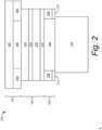
- Fig. 2 illustrates a stacked-layer view 200 of the light-sealing gasket 106 with crossbar force distribution.
- the display module 104 includes at least a panel layer 202 and a copper layer 204.
- the panel layer 202 may be stacked on an opposing side of the copper layer 204 from the second section 106-2.
- the display module 104 may include additional layers (e.g., glass layer, embossed layer), which, for simplicity of discussion, are not represented in this illustration.
- the copper layer 204 has a portion removed to define a gap (e.g., air gap 206) in the copper layer 204, which exposes a portion of the panel layer 202.
- the panel layer 202 may be delicate and receive cosmetic defects (e.g., dimples, abrasions, cracks) with less than 10 grams of force applied to it.
- the copper layer 204 is capable of withstanding much larger forces being applied.
- the gasket 106 can be assembled in multiple stacked layers.
- the first section 106-1 may include a structural layer 208 and an adhesive layer 210.
- the adhesive layer affixes the gasket 106 to the interposer layer 118.
- the structural layer 208 frames the sensor package 108, providing a base for the second section 106-2.
- the structural layer 208 may be composed of hard rubber, stiff foam, epoxy resins, plastic (e.g., polyvinyl chloride (PVC), polyethylene (PE), polyethylene terephthalate (PET), polypropylene (PP)), or any other material having structural properties that enable the structural layer 208 to provide structural support to the gasket 106 under a load.
- PVC polyvinyl chloride
- PE polyethylene
- PET polyethylene terephthalate
- PP polypropylene
- One example material used to compose the structural layer may have a compression force deflection of 259 to 279 kPa, though other materials having other ranges of compression force deflection may also be used, such as a material having a compression force deflection of 150 to 300 kPa or another with 280 to 450 kPa, to name just three examples.
- the second section 106-2 may include adhesive layers 212 and 214, a compressible layer 216, and a rigid layer 218, and have a height configured to span the distance 122 between the sensor package 108 and the display module 104.
- the rigid layer 218 (e.g., composed of a metal material) may be configured to abut the copper layer 204 of the display module 104 but does not intrude into the air gap 206. By contacting the copper layer 204 and not the panel layer 202, the rigid layer 218 applies no force to the panel layer 202, avoiding potential damage to the panel layer 202.
- the rigid layer 218 may be bonded to the compressible layer 216 by the adhesive layer 214.
- the rigid layer 218, compressible layer 216, and the adhesive layers 212 and 214 may be composed of a signal-blocking material, which shield transmit signals of the transmit module 110 and receive signals of the receive module 112 from one another.
- the rigid layer 218 may be composed of a metal material (e.g., stainless steel, aluminum) or other material that is reflective. To reduce reflectivity of the transmit signals and receive signals from the reflective material, the rigid layer 218 may receive further processing.
- the reflective material may be coated with a non-reflective material.
- the metal material may be painted a non-reflective color. Additionally or alternatively, the surface of the reflective material may be physically altered (e.g., scored, coarsened) to reduce reflections.
- the compressible layer 216 maintains a load on the rigid layer 218 and ensures the rigid layer 218 maintains contact with the copper layer 204 of the display module 104. By maintaining contact with the copper layer 204 and spanning the air gap 206, no load is applied to the panel layer 202. This protects the panel layer 202 from defects and damage. Likewise, the air gap 206 is minimized, further shielding the signals.
- the compressible layer 216 may be adhered to the first section 106-1 (e.g., the structural layer 208 of the first section 106-1) by the adhesive layer 212.
- the compressible layer 216 may be composed of any suitable material, including an elastomeric material. Some example materials may include a spongy foam, natural or synthetic soft rubber, and silicone-based materials. One example material used to compose the compressible layer may have a compression force deflection of 4.0 to 5.0 kPa, though other materials having other ranges of compression force deflection may also be used, such as a material having a compression force deflection of 3.0 to 4.4 kPa or another with 4.3 to 6 kPa, to name just three examples.
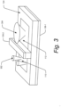
- Fig. 3 illustrates the light-sealing gasket 106 with crossbar force distribution shielding transmit signals 302 and receive signals 304 from one another.
- a display module e.g., the display module 104
- the second section 106-2 separates a volume (e.g., the volume 114 from Fig. 1-1 ) through which the transmit signals 302 propagate from a volume (e.g., the volume 116 from Fig. 1-1 ) through which the receive signals 304 propagate. In this manner, the transmit signals 302 and the receive signals 304 may not interfere with one another.
- Fig. 4-1 illustrates an example implementation 400-1 of the light-sealing gasket 106 with crossbar force distribution.
- the gasket 106 includes the first section 106-1 and a second section 404 (e.g., the second section 120-2).
- the second section 404 is represented as a beam (e.g., crossbar) assembled to the first surface 124 of the first section 106-1 and spanning across an opening (e.g., opening 408 having a center axis 410) defined by the first section 106-1.
- the first section 106-1 may define the opening 408 as any suitable two-dimensional shape in its top-down view, including a rectangular shape, a square shape, an elliptical shape, a hexagonal shape, and so forth.
- the shape of the opening 408 may be defined to substantially frame or border the sides of the sensor package 108 (shown in Fig. 1 ) that are substantially orthogonal to a front of the sensor package 108 (the front being the side of the sensor package 108 where the transmit signals 302 are output and the receive signals 304 are input). Accordingly, the shape of the opening 408 defined by the first section 106-1 of the gasket 106 may substantially match the shape of the sensor package 108, which may be any suitable shape in its top-down view.
- the second section 404 divides a volume into two volumes (e.g., the volumes 114 and 116, which are proximate to the transmit module 110 and the receive module 112, respectively, as illustrated in Fig. 1 ).
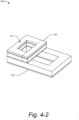
- Fig. 4-2 illustrates another example implementation 400-2 of the light-sealing gasket 106 with crossbar force distribution and a frame around the volume 114 located in front of the transmit module 110 of the sensor package 108.
- the gasket 106 has the first section 106-1 and a second section 404 (e.g., the second section 106-2).
- the second section 404 includes a frame 412 and encloses a volume (e.g., the volume 114 from Fig. 1-1 in front of the transmit module 110).
- the frame 412 can shield other components of an electronic device (e.g., the electronic device 102) from transmit signals (e.g., the transmit signals 302).
- the frame 412 may also provide additional stability to the second section 404.
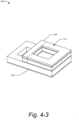
- Fig. 4-3 illustrates another example implementation 400-3 of a light-sealing gasket 106 with crossbar force distribution and a frame around the volume 116 located in front of the receive module 112 of the sensor package 108.
- the gasket 106 has the first section 106-1 and the second section 404 (e.g., the second section 106-2).
- the second section 404 includes a frame 414 and encloses a volume (e.g., the volume 116 from Fig. 1-1 ).
- the frame 414 shields the receive module 112 from any spurious signals that may be emitted by other components of an electronic device (e.g., the electronic device 102). Likewise, the frame 414 may provide additional stability to the second section 404.
- Fig. 4-4 illustrates another example implementation 400-4 of a light-sealing gasket 106 with crossbar force distribution and frames around the volumes located in front of the transmit module 110 and the receive module 112 of the sensor package 108.
- the gasket 106 has the first section 106-1 and a second section 404 (e.g., the second section 106-2).
- the second section 404 includes the frame 412 and the frame 414.
- Implementing both of the frames 412 and 414 may shield the transmit signals 302 and the receive signals 304 (shown in Fig. 3 ) from one another and from other components of the electronic device 102 (shown in Fig. 1 ). Additionally, the frames 412 and 414 may provide structural support around a complete perimeter of the second section 404.
Landscapes
- Engineering & Computer Science (AREA)
- Microelectronics & Electronic Packaging (AREA)
- Signal Processing (AREA)
- Devices For Indicating Variable Information By Combining Individual Elements (AREA)
- Shielding Devices Or Components To Electric Or Magnetic Fields (AREA)
- Casings For Electric Apparatus (AREA)
Claims (12)
- Joint (106) de protection contre les signaux de transmission et de réception d'un boîtier de capteur (108) positionné sous un module d'affichage (104) d'un dispositif électronique (102), le joint (106) comprenant :une première section (106-1) formant un cadre autour d'une ouverture avec un axe central, le cadre étant configuré pour s'enrouler autour du boîtier de capteur (108) lorsque le boîtier de capteur (108) est positionné à l'intérieur de l'ouverture, la première section (106-1) ayant une première surface (124) définissant un plan qui est sensiblement orthogonal à l'axe central ; etune seconde section (106-2) assemblée à la première surface (124) de la première section (106-1), la seconde section (106-2) ayant une hauteur configurée pour couvrir une distance (122) entre le boîtier de capteur (108) et le module d'affichage (104) du dispositif électronique (102), la seconde section (106-2) étant configurée pour :se prolonger à travers l'ouverture de la première section (106-1) au niveau d'un emplacement entre un module de transmission (110) du boîtier de capteur (108) et un module de réception (112) du boîtier de capteur (108) ;venir en butée contre le module d'affichage (104) du dispositif électronique (102) ; etprotéger les signaux de transmission (302) du module de transmission (110) des signaux de réception (304) du module de réception (112), etdans lequel la seconde section (106-2) forme une poutre à travers l'ouverture et comporte :une couche compressible (216) ;une couche rigide (218) ; etune couche adhésive (214) liant la couche compressible (216) à la couche rigide (218), etdans lequel la seconde section (106-2) est configurée pour :couvrir un espace (206) dans une couche de cuivre (204) du module d'affichage (104) ; etappliquer une charge à la couche de cuivre (204) sans appliquer de charge à travers l'espace (206) à une couche de panneau (202) du module d'affichage (104) qui est empilée sur un côté opposé de la couche de cuivre (204) à partir de la seconde section (106-2), dans lequel la couche rigide (218) est configurée pour venir en butée contre la couche de cuivre (204) du module d'affichage (104) sur des côtés opposés de l'espace (206).
- Joint (106) selon la revendication 1, dans lequel la couche compressible (216) est positionnée entre la couche rigide (218) et la première surface (124) de la première section (106-1).
- Joint (106) selon l'une quelconque des revendications précédentes, dans lequel la couche compressible (216) maintient une charge sur la couche rigide (218) pour amener la couche rigide (218) à maintenir le contact avec la couche de cuivre (204) du module d'affichage (104).
- Joint (106) selon l'une quelconque des revendications précédentes, dans lequel la seconde section (106-2) est assemblée à la première surface (124) de la première section (106-1) via une couche adhésive (212).
- Joint (106) selon l'une quelconque des revendications précédentes, dans lequel la première section (106-1) comporte une couche structurelle (208) pour fournir un support d'alignement pour le boîtier de capteur (108).
- Joint (106) selon l'une quelconque des revendications précédentes, dans lequel la couche rigide (218) comprend un matériau métallique.
- Joint (106) selon l'une quelconque des revendications précédentes, dans lequel la couche rigide (218) est revêtue pour réduire la réflectivité des signaux de transmission (302) et des signaux de réception (304).
- Joint (106) selon l'une quelconque des revendications précédentes, dans lequel la seconde section (106-2) forme un cadre autour d'un volume (114) entre le module de transmission (110) et le module d'affichage (104).
- Joint (106) selon l'une quelconque des revendications précédentes, dans lequel la seconde section (106-2) forme un cadre autour d'un volume (116) entre le module de réception (112) et le module d'affichage (104).
- Joint (106) selon l'une quelconque des revendications 1 à 6, dans lequel la seconde section (106-2) est une traverse.
- Joint (106) selon l'une quelconque des revendications précédentes, dans lequel la couche rigide (218) et la couche compressible (216) sont composées de matériaux bloquant les signaux.
- Dispositif électronique (102) comprenant :un module d'affichage (104) pour afficher un contenu multimédia, le module d'affichage (104) comportant une couche de cuivre (204) et une couche de panneau (202), la couche de cuivre (204) définissant un espace (206) qui expose une partie de la couche de panneau (202) ;un boîtier de capteur (108) positionné sous le module d'affichage (104) sur un côté de la couche de cuivre (204) opposé à la couche de panneau (202), le boîtier de capteur (108) ayant un module de transmission (110) et un module de réception (112) ; etun joint (106) tel que décrit selon l'une quelconque des revendications précédentes.
Applications Claiming Priority (1)
| Application Number | Priority Date | Filing Date | Title |
|---|---|---|---|
| PCT/US2021/017726 WO2022173437A1 (fr) | 2021-02-11 | 2021-02-11 | Joint d'étanchéité léger à distribution de force transversale |
Publications (2)
| Publication Number | Publication Date |
|---|---|
| EP4070632A1 EP4070632A1 (fr) | 2022-10-12 |
| EP4070632B1 true EP4070632B1 (fr) | 2025-04-30 |
Family
ID=74867621
Family Applications (1)
| Application Number | Title | Priority Date | Filing Date |
|---|---|---|---|
| EP21711081.6A Active EP4070632B1 (fr) | 2021-02-11 | 2021-02-11 | Joint d'étanchéité léger à distribution de force transversale |
Country Status (4)
| Country | Link |
|---|---|
| US (1) | US11974418B2 (fr) |
| EP (1) | EP4070632B1 (fr) |
| CN (1) | CN115428600A (fr) |
| WO (1) | WO2022173437A1 (fr) |
Family Cites Families (21)
| Publication number | Priority date | Publication date | Assignee | Title |
|---|---|---|---|---|
| TWI322661B (en) * | 2006-05-19 | 2010-03-21 | Asustek Comp Inc | Electromagnetic sheilding device and method of fabricating the same |
| US7288727B1 (en) * | 2006-05-31 | 2007-10-30 | Motorola, Inc. | Shield frame for a radio frequency shielding assembly |
| KR101483176B1 (ko) * | 2008-01-02 | 2015-01-16 | 삼성디스플레이 주식회사 | 개스킷과 스크린 스페이서 및 이들을 포함하는 표시 장치 |
| US20120019015A1 (en) | 2010-07-22 | 2012-01-26 | Trader Frederick E | Lift assist device |
| US9075567B2 (en) * | 2012-06-08 | 2015-07-07 | Apple Inc. | Electronic device display structures |
| US9223349B2 (en) * | 2012-06-20 | 2015-12-29 | Apple Inc. | Low-force dust seal |
| US9523586B2 (en) | 2015-03-06 | 2016-12-20 | Itron Global Sarl | Methods and apparatus for sealed communication interfaces |
| US9898054B2 (en) * | 2016-02-12 | 2018-02-20 | Apple Inc. | Near zero force grounding feature |
| US10299416B2 (en) * | 2016-06-28 | 2019-05-21 | Microsoft Technology Licensing, Llc | Shield for electronic components |
| EP3544468B1 (fr) | 2017-02-10 | 2022-01-05 | Golden Technologies, Inc. | Fauteuil inclinable ou fauteuil basculeur et inclinable à profil d'élévation variable |
| CN206490707U (zh) * | 2017-03-02 | 2017-09-12 | 广东欧珀移动通信有限公司 | 显示屏以及电子设备 |
| US20180373913A1 (en) | 2017-06-26 | 2018-12-27 | Qualcomm Incorporated | Ultrasonic fingerprint sensor for under-display applications |
| US10911656B2 (en) | 2017-11-21 | 2021-02-02 | Microsoft Technology Licensing, Llc | Optical isolation systems for displays |
| CN108769296B (zh) * | 2018-03-21 | 2020-08-07 | Oppo广东移动通信有限公司 | 电子装置及电子装置的制造方法 |
| CN108989494B (zh) * | 2018-06-27 | 2021-02-09 | 北京小米移动软件有限公司 | 一种电子设备 |
| CN108924304B (zh) * | 2018-07-16 | 2019-08-09 | Oppo广东移动通信有限公司 | 电子设备 |
| US20200022290A1 (en) * | 2018-07-16 | 2020-01-16 | Laird Technologies (Shenzhen) Ltd. | Shields |
| CN111129074B (zh) * | 2018-10-30 | 2022-07-15 | 北京小米移动软件有限公司 | 显示屏和电子设备 |
| KR102655179B1 (ko) * | 2019-07-18 | 2024-04-05 | 삼성전자주식회사 | 디스플레이 배면에 실장되는 광 센서를 포함하는 전자 장치 |
| US12028975B2 (en) * | 2020-11-09 | 2024-07-02 | Samsung Electronics Co., Ltd. | Electronic device including shielding member |
| US12133322B2 (en) * | 2020-12-23 | 2024-10-29 | Intel Corporation | Electromagnetic interference shields having attentuation interfaces |
-
2021
- 2021-02-11 EP EP21711081.6A patent/EP4070632B1/fr active Active
- 2021-02-11 CN CN202180007391.8A patent/CN115428600A/zh active Pending
- 2021-02-11 US US17/785,320 patent/US11974418B2/en active Active
- 2021-02-11 WO PCT/US2021/017726 patent/WO2022173437A1/fr not_active Ceased
Also Published As
| Publication number | Publication date |
|---|---|
| US11974418B2 (en) | 2024-04-30 |
| EP4070632A1 (fr) | 2022-10-12 |
| US20230354567A1 (en) | 2023-11-02 |
| WO2022173437A1 (fr) | 2022-08-18 |
| CN115428600A (zh) | 2022-12-02 |
Similar Documents
| Publication | Publication Date | Title |
|---|---|---|
| KR102702247B1 (ko) | 음향 모듈을 포함하는 전자 장치 | |
| KR102461205B1 (ko) | 휴대용 전자 디바이스 | |
| TWI524113B (zh) | 顯示裝置 | |
| EP2447762B1 (fr) | Appareil d'affichage | |
| KR20220026565A (ko) | 보호 필름 제조 방법 및 표시 장치 제조 방법 | |
| EP4018631B1 (fr) | Terminal portable ayant un haut-parleur et trajet de sortie acoustique pour haut-parleur | |
| EP2774137B1 (fr) | Construction résistant aux impacts d'un dispositif interactif | |
| US9119287B2 (en) | Display device and electronic apparatus | |
| WO2014083692A1 (fr) | Appareil d'affichage | |
| US9885899B2 (en) | Display device | |
| EP3342069B1 (fr) | Protection par l'intermédiaire d'un châssis d'affichage | |
| KR20190094982A (ko) | 전자 장치 | |
| US20140036458A1 (en) | Electronic apparatus | |
| WO2014020937A1 (fr) | Appareil électronique | |
| US20240179859A1 (en) | Trimless Foldable Displays | |
| EP4070632B1 (fr) | Joint d'étanchéité léger à distribution de force transversale | |
| EP3086535B1 (fr) | Dispositif mobile avec un écran agrandit | |
| KR101903398B1 (ko) | 디스플레이 장치 | |
| JP6530949B2 (ja) | 医療用モニター、電子機器、及び映像表示ユニット | |
| EP3761107B1 (fr) | Appareil d'affichage | |
| US9785003B2 (en) | Electronic device | |
| KR102715535B1 (ko) | 초음파 센서를 포함하는 표시 장치 | |
| US20250180799A1 (en) | Display module and electronic device | |
| US10353140B2 (en) | Backlight unit and display device | |
| KR101839377B1 (ko) | 표시 장치 |
Legal Events
| Date | Code | Title | Description |
|---|---|---|---|
| STAA | Information on the status of an ep patent application or granted ep patent |
Free format text: STATUS: UNKNOWN |
|
| STAA | Information on the status of an ep patent application or granted ep patent |
Free format text: STATUS: THE INTERNATIONAL PUBLICATION HAS BEEN MADE |
|
| PUAI | Public reference made under article 153(3) epc to a published international application that has entered the european phase |
Free format text: ORIGINAL CODE: 0009012 |
|
| STAA | Information on the status of an ep patent application or granted ep patent |
Free format text: STATUS: REQUEST FOR EXAMINATION WAS MADE |
|
| 17P | Request for examination filed |
Effective date: 20220623 |
|
| AK | Designated contracting states |
Kind code of ref document: A1 Designated state(s): AL AT BE BG CH CY CZ DE DK EE ES FI FR GB GR HR HU IE IS IT LI LT LU LV MC MK MT NL NO PL PT RO RS SE SI SK SM TR |
|
| DAV | Request for validation of the european patent (deleted) | ||
| DAX | Request for extension of the european patent (deleted) | ||
| GRAP | Despatch of communication of intention to grant a patent |
Free format text: ORIGINAL CODE: EPIDOSNIGR1 |
|
| STAA | Information on the status of an ep patent application or granted ep patent |
Free format text: STATUS: GRANT OF PATENT IS INTENDED |
|
| INTG | Intention to grant announced |
Effective date: 20241122 |
|
| GRAS | Grant fee paid |
Free format text: ORIGINAL CODE: EPIDOSNIGR3 |
|
| GRAA | (expected) grant |
Free format text: ORIGINAL CODE: 0009210 |
|
| STAA | Information on the status of an ep patent application or granted ep patent |
Free format text: STATUS: THE PATENT HAS BEEN GRANTED |
|
| AK | Designated contracting states |
Kind code of ref document: B1 Designated state(s): AL AT BE BG CH CY CZ DE DK EE ES FI FR GB GR HR HU IE IS IT LI LT LU LV MC MK MT NL NO PL PT RO RS SE SI SK SM TR |
|
| P01 | Opt-out of the competence of the unified patent court (upc) registered |
Free format text: CASE NUMBER: APP_13829/2025 Effective date: 20250320 |
|
| REG | Reference to a national code |
Ref country code: CH Ref legal event code: EP Ref country code: GB Ref legal event code: FG4D |
|
| REG | Reference to a national code |
Ref country code: IE Ref legal event code: FG4D |
|
| REG | Reference to a national code |
Ref country code: DE Ref legal event code: R096 Ref document number: 602021029978 Country of ref document: DE |
|
| REG | Reference to a national code |
Ref country code: NL Ref legal event code: MP Effective date: 20250430 |
|
| REG | Reference to a national code |
Ref country code: AT Ref legal event code: MK05 Ref document number: 1791322 Country of ref document: AT Kind code of ref document: T Effective date: 20250430 |
|
| PG25 | Lapsed in a contracting state [announced via postgrant information from national office to epo] |
Ref country code: FI Free format text: LAPSE BECAUSE OF FAILURE TO SUBMIT A TRANSLATION OF THE DESCRIPTION OR TO PAY THE FEE WITHIN THE PRESCRIBED TIME-LIMIT Effective date: 20250430 Ref country code: PT Free format text: LAPSE BECAUSE OF FAILURE TO SUBMIT A TRANSLATION OF THE DESCRIPTION OR TO PAY THE FEE WITHIN THE PRESCRIBED TIME-LIMIT Effective date: 20250901 Ref country code: ES Free format text: LAPSE BECAUSE OF FAILURE TO SUBMIT A TRANSLATION OF THE DESCRIPTION OR TO PAY THE FEE WITHIN THE PRESCRIBED TIME-LIMIT Effective date: 20250430 |
|
| REG | Reference to a national code |
Ref country code: LT Ref legal event code: MG9D |
|
| PG25 | Lapsed in a contracting state [announced via postgrant information from national office to epo] |
Ref country code: GR Free format text: LAPSE BECAUSE OF FAILURE TO SUBMIT A TRANSLATION OF THE DESCRIPTION OR TO PAY THE FEE WITHIN THE PRESCRIBED TIME-LIMIT Effective date: 20250731 Ref country code: NO Free format text: LAPSE BECAUSE OF FAILURE TO SUBMIT A TRANSLATION OF THE DESCRIPTION OR TO PAY THE FEE WITHIN THE PRESCRIBED TIME-LIMIT Effective date: 20250730 |
|
| PG25 | Lapsed in a contracting state [announced via postgrant information from national office to epo] |
Ref country code: NL Free format text: LAPSE BECAUSE OF FAILURE TO SUBMIT A TRANSLATION OF THE DESCRIPTION OR TO PAY THE FEE WITHIN THE PRESCRIBED TIME-LIMIT Effective date: 20250430 Ref country code: PL Free format text: LAPSE BECAUSE OF FAILURE TO SUBMIT A TRANSLATION OF THE DESCRIPTION OR TO PAY THE FEE WITHIN THE PRESCRIBED TIME-LIMIT Effective date: 20250430 |
|
| PG25 | Lapsed in a contracting state [announced via postgrant information from national office to epo] |
Ref country code: BG Free format text: LAPSE BECAUSE OF FAILURE TO SUBMIT A TRANSLATION OF THE DESCRIPTION OR TO PAY THE FEE WITHIN THE PRESCRIBED TIME-LIMIT Effective date: 20250430 |
|
| PG25 | Lapsed in a contracting state [announced via postgrant information from national office to epo] |
Ref country code: HR Free format text: LAPSE BECAUSE OF FAILURE TO SUBMIT A TRANSLATION OF THE DESCRIPTION OR TO PAY THE FEE WITHIN THE PRESCRIBED TIME-LIMIT Effective date: 20250430 |
|
| PG25 | Lapsed in a contracting state [announced via postgrant information from national office to epo] |
Ref country code: AT Free format text: LAPSE BECAUSE OF FAILURE TO SUBMIT A TRANSLATION OF THE DESCRIPTION OR TO PAY THE FEE WITHIN THE PRESCRIBED TIME-LIMIT Effective date: 20250430 |
|
| PG25 | Lapsed in a contracting state [announced via postgrant information from national office to epo] |
Ref country code: RS Free format text: LAPSE BECAUSE OF FAILURE TO SUBMIT A TRANSLATION OF THE DESCRIPTION OR TO PAY THE FEE WITHIN THE PRESCRIBED TIME-LIMIT Effective date: 20250731 |
|
| PG25 | Lapsed in a contracting state [announced via postgrant information from national office to epo] |
Ref country code: IS Free format text: LAPSE BECAUSE OF FAILURE TO SUBMIT A TRANSLATION OF THE DESCRIPTION OR TO PAY THE FEE WITHIN THE PRESCRIBED TIME-LIMIT Effective date: 20250830 |
|
| PG25 | Lapsed in a contracting state [announced via postgrant information from national office to epo] |
Ref country code: LV Free format text: LAPSE BECAUSE OF FAILURE TO SUBMIT A TRANSLATION OF THE DESCRIPTION OR TO PAY THE FEE WITHIN THE PRESCRIBED TIME-LIMIT Effective date: 20250430 |
|
| PG25 | Lapsed in a contracting state [announced via postgrant information from national office to epo] |
Ref country code: SM Free format text: LAPSE BECAUSE OF FAILURE TO SUBMIT A TRANSLATION OF THE DESCRIPTION OR TO PAY THE FEE WITHIN THE PRESCRIBED TIME-LIMIT Effective date: 20250430 Ref country code: DK Free format text: LAPSE BECAUSE OF FAILURE TO SUBMIT A TRANSLATION OF THE DESCRIPTION OR TO PAY THE FEE WITHIN THE PRESCRIBED TIME-LIMIT Effective date: 20250430 |
|
| PG25 | Lapsed in a contracting state [announced via postgrant information from national office to epo] |
Ref country code: CZ Free format text: LAPSE BECAUSE OF FAILURE TO SUBMIT A TRANSLATION OF THE DESCRIPTION OR TO PAY THE FEE WITHIN THE PRESCRIBED TIME-LIMIT Effective date: 20250430 |
|
| PG25 | Lapsed in a contracting state [announced via postgrant information from national office to epo] |
Ref country code: EE Free format text: LAPSE BECAUSE OF FAILURE TO SUBMIT A TRANSLATION OF THE DESCRIPTION OR TO PAY THE FEE WITHIN THE PRESCRIBED TIME-LIMIT Effective date: 20250430 |
|
| PG25 | Lapsed in a contracting state [announced via postgrant information from national office to epo] |
Ref country code: SK Free format text: LAPSE BECAUSE OF FAILURE TO SUBMIT A TRANSLATION OF THE DESCRIPTION OR TO PAY THE FEE WITHIN THE PRESCRIBED TIME-LIMIT Effective date: 20250430 |
|
| PG25 | Lapsed in a contracting state [announced via postgrant information from national office to epo] |
Ref country code: IT Free format text: LAPSE BECAUSE OF FAILURE TO SUBMIT A TRANSLATION OF THE DESCRIPTION OR TO PAY THE FEE WITHIN THE PRESCRIBED TIME-LIMIT Effective date: 20250430 |
|
| REG | Reference to a national code |
Ref country code: DE Ref legal event code: R097 Ref document number: 602021029978 Country of ref document: DE |
|
| PLBE | No opposition filed within time limit |
Free format text: ORIGINAL CODE: 0009261 |
|
| STAA | Information on the status of an ep patent application or granted ep patent |
Free format text: STATUS: NO OPPOSITION FILED WITHIN TIME LIMIT |
|
| REG | Reference to a national code |
Ref country code: CH Ref legal event code: L10 Free format text: ST27 STATUS EVENT CODE: U-0-0-L10-L00 (AS PROVIDED BY THE NATIONAL OFFICE) Effective date: 20260311 |
|
| 26N | No opposition filed |
Effective date: 20260202 |
|
| PGFP | Annual fee paid to national office [announced via postgrant information from national office to epo] |
Ref country code: DE Payment date: 20260227 Year of fee payment: 6 |