EP4071948B1 - Module de distribution d'énergie et système d'alimentation électrique de communication - Google Patents
Module de distribution d'énergie et système d'alimentation électrique de communication Download PDFInfo
- Publication number
- EP4071948B1 EP4071948B1 EP20904357.9A EP20904357A EP4071948B1 EP 4071948 B1 EP4071948 B1 EP 4071948B1 EP 20904357 A EP20904357 A EP 20904357A EP 4071948 B1 EP4071948 B1 EP 4071948B1
- Authority
- EP
- European Patent Office
- Prior art keywords
- signal
- circuit breaker
- module
- battery
- slot
- Prior art date
- Legal status (The legal status is an assumption and is not a legal conclusion. Google has not performed a legal analysis and makes no representation as to the accuracy of the status listed.)
- Active
Links
Images




Classifications
-
- H—ELECTRICITY
- H02—GENERATION; CONVERSION OR DISTRIBUTION OF ELECTRIC POWER
- H02B—BOARDS, SUBSTATIONS OR SWITCHING ARRANGEMENTS FOR THE SUPPLY OR DISTRIBUTION OF ELECTRIC POWER
- H02B1/00—Frameworks, boards, panels, desks, casings; Details of substations or switching arrangements
- H02B1/015—Boards, panels, desks; Parts thereof or accessories therefor
- H02B1/04—Mounting thereon of switches or of other devices in general, the switch or device having, or being without, casing
- H02B1/056—Mounting on plugboards
-
- H—ELECTRICITY
- H02—GENERATION; CONVERSION OR DISTRIBUTION OF ELECTRIC POWER
- H02B—BOARDS, SUBSTATIONS OR SWITCHING ARRANGEMENTS FOR THE SUPPLY OR DISTRIBUTION OF ELECTRIC POWER
- H02B1/00—Frameworks, boards, panels, desks, casings; Details of substations or switching arrangements
- H02B1/20—Bus-bar or other wiring layouts, e.g. in cubicles, in switchyards
- H02B1/205—Bus-bar or other wiring layouts, e.g. in cubicles, in switchyards for connecting electrical apparatus mounted side by side on a rail
-
- H—ELECTRICITY
- H01—ELECTRIC ELEMENTS
- H01H—ELECTRIC SWITCHES; RELAYS; SELECTORS; EMERGENCY PROTECTIVE DEVICES
- H01H71/00—Details of the protective switches or relays covered by groups H01H73/00 - H01H83/00
- H01H71/02—Housings; Casings; Bases; Mountings
- H01H71/0264—Mountings or coverplates for complete assembled circuit breakers, e.g. snap mounting in panel
-
- H—ELECTRICITY
- H02—GENERATION; CONVERSION OR DISTRIBUTION OF ELECTRIC POWER
- H02B—BOARDS, SUBSTATIONS OR SWITCHING ARRANGEMENTS FOR THE SUPPLY OR DISTRIBUTION OF ELECTRIC POWER
- H02B1/00—Frameworks, boards, panels, desks, casings; Details of substations or switching arrangements
- H02B1/015—Boards, panels, desks; Parts thereof or accessories therefor
- H02B1/04—Mounting thereon of switches or of other devices in general, the switch or device having, or being without, casing
- H02B1/056—Mounting on plugboards
- H02B1/0565—Mounting on plugboards by means of an adapter carrying one or more apparatuses
-
- H—ELECTRICITY
- H02—GENERATION; CONVERSION OR DISTRIBUTION OF ELECTRIC POWER
- H02J—ELECTRIC POWER NETWORKS; CIRCUIT ARRANGEMENTS OR SYSTEMS FOR SUPPLYING OR DISTRIBUTING ELECTRIC POWER; SYSTEMS FOR STORING ELECTRIC ENERGY
- H02J1/00—Circuit arrangements for DC mains or DC distribution networks
- H02J1/10—Parallel operation of DC sources
-
- H—ELECTRICITY
- H05—ELECTRIC TECHNIQUES NOT OTHERWISE PROVIDED FOR
- H05K—PRINTED CIRCUITS; CASINGS OR CONSTRUCTIONAL DETAILS OF ELECTRIC APPARATUS; MANUFACTURE OF ASSEMBLAGES OF ELECTRICAL COMPONENTS
- H05K7/00—Constructional details common to different types of electric apparatus
- H05K7/14—Mounting supporting structure in casing or on frame or rack
- H05K7/1438—Back panels or connecting means therefor; Terminals; Coding means to avoid wrong insertion
- H05K7/1457—Power distribution arrangements
-
- H—ELECTRICITY
- H02—GENERATION; CONVERSION OR DISTRIBUTION OF ELECTRIC POWER
- H02J—ELECTRIC POWER NETWORKS; CIRCUIT ARRANGEMENTS OR SYSTEMS FOR SUPPLYING OR DISTRIBUTING ELECTRIC POWER; SYSTEMS FOR STORING ELECTRIC ENERGY
- H02J9/00—Circuit arrangements for emergency or stand-by power supply, e.g. for emergency lighting
- H02J9/04—Circuit arrangements for emergency or stand-by power supply, e.g. for emergency lighting in which the distribution system is disconnected from the normal source and connected to a standby source
- H02J9/06—Circuit arrangements for emergency or stand-by power supply, e.g. for emergency lighting in which the distribution system is disconnected from the normal source and connected to a standby source with automatic change-over, e.g. UPS systems
- H02J9/061—Circuit arrangements for emergency or stand-by power supply, e.g. for emergency lighting in which the distribution system is disconnected from the normal source and connected to a standby source with automatic change-over, e.g. UPS systems for DC powered loads
Definitions
- This application relates to the field of communication power supply circuit technologies, and in particular, to a power distribution module and a communication power supply system.
- Loads of a communication power supply system generally include a primary load and a secondary load. When there is no mains supply, a standby power supply such as a battery is used. A primary load, a secondary load, and a battery are powered on and off by controlling corresponding circuit breakers by a contactor. Based on functionality of branches to which circuit breakers belong, copper bars to be connected to the circuit breakers need to be manufactured into sectional type copper bars each with a matched function area, to limit a quantity of circuit breakers to be installed in each function area and function allocation of the function area.
- EP 0 252 512 A1 discloses a multiple plug connection unit for the power supply of one or more parallel-connected loads having busbars for phase, neutral and earth connection arranged parallel to one another in a base strip of dielectric material, and in each case with an overcurrent circuit breaker which can be inserted between the phase busbar and the respective load.
- the loads are in each case connected via distribution lines which can be electrically connected to the relevant busbars by means of the multiple plug connection unit.
- the busbars are surrounded on all sides by the housing of the base strip and are accessible for contact tongues through plug-in openings which are arranged in a housing wall and are essentially flush in each case with the busbars.
- the distribution line terminals for each load are in each case collected in a separate terminal block.
- the terminal blocks are arranged in a row along the base strip and can be placed thereon providing a direct contact with the neutral and earth busbars.
- the overcurrent circuit breakers can be placed on the housing of the base strip making contact with the phase busbar and simultaneously, when they are in position, in each case make contact with the phase terminals of the terminal blocks enclosed between the base strip and the overcurrent circuit breaker.
- US 6 315 580 B1 discloses a connector module for overcurrent protection devices uses a printed circuit board substrate as a support surface for line and load busbar members and auxiliary signal clip connectors disposed on one side of the substrate. Passageways in the substrate enable male current plugs to extend through the substrate to mate with sockets disposed in the busbars. Additional passageways enable auxiliary contact terminals to extend through the substrate. Clip connectors disposed on the substrate are used to make electrical contact to the auxiliary terminals.
- the sockets and clips are shaped and dimensioned to mate with the current and alarm contact terminals of a plug-in circuit breaker.
- Implementations of this application intend to resolve a technical problem of providing a power distribution module and a communication power supply system that can improve installation flexibility of a circuit breaker.
- the present invention provides a communication power supply system according to claim 1. Preferred embodiments are disclosed in the dependent claims.
- the power distribution module in this application power is obtained by using the power busbar, the circuit breaker signal collected by the signal-driven collection module is fed back to a monitoring module, to control on and off (namely, powering off and on) of the circuit breaker of each of the primary load output module, the secondary load output module, and the battery module, monitoring of a status of the circuit breaker, and the like.
- no contactor is used for powering on and off and no current divider is used for current division. Therefore, no distinction is made on physical hardware between function areas accessed by a primary load, a secondary load, a battery, and the like.
- an integer quantity of first signal units are disposed in the connection area in which the signal-driven collection module is connected to the circuit breaker.
- the circuit breaker is disposed in the first direction in a manner of corresponding to an integer quantity of first signal units of the signal-driven collection module, for example, one or two, so that hybrid connection between the signal-driven collection module and the circuit breakers of the primary load output module, the secondary load output module, and the battery module is implemented without limitation, thereby reducing secondary design and development due to users' requirements for a capacity and a quantity of circuit breakers in function areas accessed by a primary load, a secondary load, a battery, and the like, and improving flexibility of layout of the power distribution module.
- FIG. 1 is a block diagram of a structure of a communication power supply system according to a first implementation of this application.
- the communication power supply system 200 includes an alternating current power distribution module 201, a rectifier module 203, a direct current power distribution module 10, and a monitoring module 207.
- the alternating current power distribution module 201 is configured to provide alternating current mains.
- the alternating current power distribution module 201 includes an alternating current power distribution unit 2011 and a lightning protection unit 2013.
- the lightning protection unit 2011 is configured to perform lightning protection detection on the alternating current power distribution unit 2011 and provide a detection result for the monitoring module 207.
- the rectifier module 203 is connected to the alternating current power distribution unit 2011 of the alternating current power distribution module 201, and is configured to: convert the alternating current mains into a direct current, and provide the direct current for the direct current power distribution module 10.
- the rectifier module 203 includes a plurality of rectifier units 2031 and a connector 2033 connected to the plurality of rectifier units 2031.
- the direct current power distribution module 10 includes a power busbar 11, a primary load output module 13, a secondary load output module 14, a battery module 15, and a signal-driven collection module 17.
- the power busbar 11 is connected to the connector 2033 of the rectifier module 203.
- Each of the primary load output module 13, the secondary load output module 14, and the battery module 15 includes a circuit breaker 19.
- the primary load output module 13 further includes a primary load 131 connected to the circuit breaker 19 of the primary load output module 13.
- the secondary load output module 14 further includes a secondary load 141 connected to the circuit breaker 19 of the secondary load output module 14.
- the battery module 15 further includes a battery 151 connected to the circuit breaker 19 of the battery module 15.
- the circuit breaker 19 of each of the primary load output module 13, the secondary load output module 14, and the battery module 15 is connected to the power busbar 11.
- the circuit breakers 19 of all function areas (accessed by the primary load 131, the secondary load 141, and the battery 151) share one power busbar 11, to simplify a structure of the direct current power distribution module 10.
- the rectifier module 203 is configured to supply power to the primary load 131, the secondary load 141, and the battery 151.
- the battery 151 is configured to supply power to the primary load 131 and the secondary load 141 when the rectifier module 203 cannot supply power.
- the primary load output module 13 includes M primary load branches 130, and each primary load branch 130 is provided with a circuit breaker 19 and a primary load 131, where M is an integer greater than or equal to 1.
- the secondary load output module 14 includes N secondary load branches 140, and each secondary load branch 140 includes a circuit breaker 19 and a secondary load 141, where N is an integer greater than or equal to 1.
- the battery module 15 includes P battery branches 150, and each battery branch 150 has a circuit breaker 19 and a battery 151, where P is an integer greater than or equal to 1.
- the signal-driven collection module 17 is connected to the circuit breaker 19 of each of the primary load output module 13, the secondary load output module 14, and the battery module 15, and is configured to collect a circuit breaker signal of the circuit breaker 19.
- the circuit breaker signal includes a switch-on signal, a switch-off signal, a circuit breaker address signal, a circuit breaker current signal, a circuit breaker voltage signal, a fault trip status signal, and the like.
- the monitoring module 207 is configured to control and monitor the circuit breaker 19 based on the circuit breaker signal collected by the signal-driven collection module 17, to improve intelligence and reliability of the communication power supply system 200. For example, when the monitoring module 207 obtains an instruction requiring a circuit breaker 19 of a specific address to be switched off, the monitoring module 207 identifies the circuit breaker 19 of the corresponding address by using a collected circuit breaker signal, and controls the circuit breaker 19 to be switched off. For another example, the monitoring module 207 may monitor a status of the circuit breakers 19 by using an obtained circuit breaker current signal, to determine whether each circuit breaker 19 can effectively switch a circuit on and off, to improve electrical safety and reliability of the communication power supply system 200.
- the signal-driven collection module 17 collects the circuit breaker signal, to not only implement a function of detecting the status of the circuit breaker, but also implement functions including controlling the circuit breaker to be switched off and on, detecting a current of the circuit breaker, collecting an address of the circuit breaker, identifying the circuit breaker, and the like, provided that the monitoring module 207 can control and monitor the circuit breaker based on the circuit breaker signal collected by the signal-driven collection module 17.
- the monitoring module 207 uses the circuit breaker signal of the circuit breaker 19 that is collected by the signal-driven collection module 17, to control on and off (namely, powering on and off) of the circuit breaker 19 of each of the primary load output module 13, the secondary load output module 14, and the battery module 15, and to monitor the status of the circuit breaker.
- the direct current power distribution module 10 does not use any contactor for powering on and off and does not use any current divider for current division. Therefore, no distinction is made on physical hardware between function areas accessed by the primary load, the secondary load, the battery, and the like, thereby improving flexibility of layout of the direct current power distribution module 10.
- the monitoring module 207 is further configured to monitor a voltage of the battery 151, to control power supplied by the battery to the primary load 131 and the secondary load 141.
- a power supply circuit for the battery 151 to supply power to the secondary load 141 is switched off.
- a power supply circuit for the battery 151 to supply power to the primary load 131 and the secondary load 141 is switched off.
- a working principle of the communication power supply system 200 shown in FIG. 1 is as follows: In a normal case, the rectifier module 203 supplies power to the primary load 131, the secondary load 141, and the battery 151. When the rectifier module 203 cannot supply power, the battery 151 supplies power to the primary load 131 and the secondary load 141.
- the voltage of the battery 151 When the voltage of the battery 151 is greater than or equal to the preset maximum threshold voltage and greater than or equal to the preset minimum threshold voltage, the voltage of the battery 151 can be used for operation of both the primary load 131 and the secondary load 141; and when the voltage of the battery 151 is greater than or equal to the preset minimum threshold voltage and less than the preset maximum threshold voltage, the voltage of the battery 151 is insufficient for operation of both the primary load 131 and the secondary load 141, but can be sufficient for operation of the primary load 131. Therefore, the monitoring module 207 controls the circuit breaker 19 on the secondary load output module 14 to be switched off, to power off the secondary load output module 14, thereby ensuring normal operation of the primary load 131.
- a quantity of circuit breakers 19 in the primary load output module 13 is not limited.
- the primary load output module 13 may include one circuit breaker 19 and M primary loads 131, and the monitoring module 207 controls the M primary loads 131 by using the circuit breaker 19.
- a quantity of circuit breakers 19 in the secondary load output module 14 is not limited.
- the secondary load output module 14 may include one circuit breaker 19 and N secondary loads 141, and the monitoring module 207 controls the N secondary loads 141 by using the circuit breaker 19.
- a quantity of circuit breakers 19 in the battery module 15 is not limited.
- the battery module 15 may include one circuit breaker 19 and P batteries 151, and the monitoring module 207 controls the P batteries 151 by using the circuit breaker 19.
- FIG. 2 is a schematic diagram of three-dimensional assembly of a direct current power distribution module according to a first implementation of this application.
- FIG. 3 is a schematic diagram of three-dimensional assembly of a circuit breaker with a power busbar and a signal-driven collection module shown in FIG. 2.
- FIG. 3 shows an example of assembling only one circuit breaker 19 with a power busbar 11 and a signal-driven collection module 17, and other circuit breakers 19 are hidden.
- the circuit breaker 19 includes a first slot 191, an insertion slot 193, and a second slot 195 that are provided at intervals in a Z direction, where the insertion slot 193 is located between the first slot 191 and the second slot 195.
- the first slot 191, the insertion slot 193, and the second slot 195 are all through slots extending in a Y direction.
- the power busbar 11 includes a positive power busbar 111 and a negative power busbar 113.
- the positive power busbar 111 is inserted into the first slot 191 to be connected to the circuit breaker 19
- the negative power busbar 113 is inserted into the second slot 195 to be connected to the circuit breaker 19
- the signal-driven collection module 17 is inserted into the insertion slot 193 to be connected to the circuit breaker 19.
- the positive power busbar 111, the negative power busbar 113, and the signal-driven collection module 17 are stacked in the Z direction, where the signal-driven collection module 17 is located between the positive power busbar 111 and the negative power busbar 113.
- FIG. 4 is a schematic diagram of a structure of a direct current power distribution module in an application scenario, where the signal-driven collection module 17 includes a plurality of signal collection boards 171.
- the plurality of signal collection boards 171 are disposed in parallel.
- FIG. 4 shows only two signal collection boards 171.
- the signal collection board 171 includes a plurality of first signal units 1711 and a plurality of guide slots 1713.
- the plurality of first signal units 1711 are sequentially arranged in a Y direction, and one guide slot 1713 is provided between every two adjacent first signal units 1711.
- the guide slot 1713 is of a guide structure used for guiding when the signal collection board 171 is inserted into the insertion slot 173, which facilitates assembly of the signal collection board 171 with the circuit breaker 19.
- the signal collection board 171 is generally comb-shaped
- the first signal unit 1711 is generally of a tooth-shaped structure
- the guide slot 1713 is of a groove structure disposed between two adjacent first signal units 1711.
- FIG. 4 shows only an example in which each signal collection board 171 includes 14 first signal units 1711.
- the plurality of first signal units 1711 have a same width, and the plurality of guide slots 1713 have a same width.
- the plurality of first signal units 1711 are disposed on the signal collection board 171 at an equal interval, which facilitates inserting the signal collection board 171 into the circuit breaker 19 for position limitation and fool-proofing. It may be understood that, that the plurality of first signal units 1711 are disposed at an equal interval is not limited, and that the plurality of guide slots 1713 have a same width is not limited.
- first signal units 1711 are disposed in a connection area 1701 in which the signal collection board 171 is connected to each circuit breaker 19.
- each circuit breaker 19 is disposed in the Y direction in a manner of corresponding to an integer quantity of first signal units 1711 of the signal-driven collection module 17, for example, one or two.
- An integer quantity of first signal units 1711 are disposed in a connection area 1701 in which the signal-driven collection board 171 is inserted into an insertion slot 193 of each circuit breaker 19, that is, each insertion slot 193 is provided in the Y direction in a manner of corresponding to an integer quantity of first signal units 1711.
- One second signal unit 194 is disposed in the insertion slot 193 of the circuit breaker 19.
- the second signal unit 194 interconnects with one first signal unit 1711 at a position corresponding to the signal collection board 1711, so that the signal collection board 171 collects a circuit breaker signal of the circuit breaker 19 and feeds back the circuit breaker signal to the monitoring module 207.
- the first signal unit 1711 is a connection terminal
- the second signal unit 194 is a connection interface or is of another structure that can implement signal transmission therebetween.
- the circuit breaker 19 includes a plurality of first circuit breakers 196 and a plurality of second circuit breakers 197.
- the first circuit breaker 196 and the second circuit breaker 197 have different widths.
- the first circuit breaker 196 is a 125A circuit breaker and the second circuit breaker 197 is a 63A circuit breaker.
- the plurality of first signal units 1711 have a same tooth width, the plurality of guide slots 1713 have a same width, and the width of the first circuit breaker 196 and the width of the second circuit breaker 197 are set in the Y direction in a manner of corresponding to an integer quantity of first signal units 1711, so that the signal collection board 171 can be installed on the first circuit breaker 196 and the second circuit breaker 197 randomly without limitation, that is, hybrid insertion of the signal collection board 171 into the circuit breakers 19 on the primary load output module 13, the secondary load output module 14, and the battery module 15 can be implemented without limitation according to arrangement of the circuit breakers 19, thereby improving freedom of the primary load 131, the secondary load 141, and the battery 151 to access the communication power supply system 200.
- W1:W2 1.5:1 is not limited, W1:W2 may be equal to another value, for example, 2:1, 1:1, 2:1, or the like.
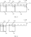
- the signal collection board 171 is assembled with three circuit breakers 19 having different widths.
- first signal units 1711 are disposed in a connection area 1701 in which the signal collection board 171 is connected to the first circuit breaker 196
- three first signal units 1711 are disposed in a connection area 1701 in which the signal collection board 171 is connected to the second circuit breaker 197
- four first signal units 171 are disposed in a connection area 1701 in which the signal collection board 171 is connected to the third circuit breaker 198.
- the signal collection board 171 is assembled with two circuit breakers 19 having different widths.
- the width W1 of the first circuit breaker 196 is approximately the same as that of one first signal unit 1711, one first signal unit 1711 is disposed in a connection area 1701 in which the signal collection board 171 is connected to the first circuit breaker 196, and two first signal units 171 are disposed in a connection area 1701 in which the signal collection board 171 is connected to the second circuit breaker 197.
- a structure of the direct current power distribution module in this implementation may also be applied to an alternating current power distribution module.
- a power distribution module includes a power busbar, a primary load output module, a secondary load output module, a battery module, and a signal-driven collection module, where each of the primary load output module, the secondary load output module, and the battery module includes a circuit breaker, the power busbar is connected to the circuit breaker, the signal-driven collection module is connected to the circuit breaker to collect a circuit breaker signal, the signal-driven collection module includes a plurality of first signal units sequentially arranged in a first direction, an integer quantity of first signal units are disposed in a connection area in which the signal-driven collection module is connected to each circuit breaker, each circuit breaker is provided with a second signal unit, and the second signal unit interconnects with one of the first signal units, implementing that the signal-driven collection module collects a circuit breaker signal of the circuit breaker and feeds back the circuit breaker signal to a
- the power busbar includes at least one of a direct current positive electrode, a direct current negative electrode, a ground bar, an alternating current L1-phase bar, an alternating current L2-phase bar, an alternating current L3-phase bar, and an alternating current N-phase bar. This is not limited herein.
- the signal-driven collection module 17 may alternatively include only one signal collection board 171. That a plurality of first signal units 1711 have a same width is not limited, and that a plurality of guide slots 1713 have a same width is not limited, that is, a plurality of first signal units 1711 are disposed on the signal collection board 171 at intervals, and an integer quantity of first signal units 1711 are disposed in a connection area 1701 in which the signal-driven collection module 17 is connected to each circuit breaker 19, provided that the second signal unit 194 interconnects with one of the integer quantity of first signal units 1711 in the connection area 1701.
- the first slot 191 is not limited to a through slot, provided that the positive power busbar 111 can be inserted into the first slot 191;
- the insertion slot 193 is not limited to a through slot, provided that the signal collection board 171 can be inserted into the insertion slot 193;
- the second slot 195 is not limited to a through slot, provided that the negative power busbar 113 can be inserted into the second slot 195.
- connection between the signal-driven collection module 17 and the circuit breaker 19 is implemented by using the insertion slot 193 is not limited, and the connection therebetween may alternatively be implemented in another manner.
- a slot is provided in the signal-driven collection module 17, and the circuit breaker 19 is provided with a plug part that can be inserted into the slot of the signal-driven collection module 17. This is not limited herein.
- FIG. 7 is a schematic planar diagram of assembly of a signal-driven collection module with a circuit breaker according to a second implementation of this application.
- FIG. 8 is a schematic planar diagram of disassembly of a signal-driven collection module from a circuit breaker shown in FIG. 7 .
- a structure of a power distribution module provided in the second implementation is generally the same as that of the direct current power distribution module 10 provided in the first implementation.
- a difference between the structures lies in that a part of a structure of a signal-driven collection module 271 and a part of a structure of a circuit breaker 29 are respectively different from those of the signal-driven collection module and the circuit breaker provided in the first implementation.
- the signal-driven collection module 271 includes a main body 2711, a plurality of first signal units 2713, and a plurality of guide pillars 2715.
- the main body 2711 includes a first surface 2721 and a second surface 2723 formed by bending and extending the first surface 2721.
- the plurality of first signal units 2713 are disposed on the first surface 2721 of the main body 2711 at an equal interval, there is a gap 2716 between every two adjacent first signal units 2713, the plurality of guide pillars 2715 are disposed on the second surface 2723 of the main body 2711 in a protruding manner at an equal interval, and each guide pillar 2715 is disposed in a manner of corresponding to one gap 2716.
- the circuit breaker 29 is provided with a second signal unit 291 and a guide slot 293 in an insertion slot (not shown in the figure), and the second signal unit 291 is configured to interconnect with the first signal unit 2713.
- Each guide pillar 2715 is inserted into one guide slot 293 in a matched manner.
- the guide pillar 2715 is disposed on the second surface 2723 in a protruding manner is not limited.
- the guide pillar 2715 may alternatively be disposed on the first surface 2721 or another surface in a protruding manner.
- the circuit breaker 29 includes a first circuit breaker 296, a second circuit breaker 297, and a third circuit breaker 298.
- the signal-driven collection module 271 is inserted into the first circuit breaker 296, the second circuit breaker 297, and the third circuit breaker 298, and the second circuit breaker 293 is located between the first circuit breaker 291 and the third circuit breaker 295.
- FIG. 9 is a schematic diagram of three-dimensional assembly of a partial structure of a power distribution module according to a third implementation of this application.
- a structure of the power distribution module provided in the third implementation is generally the same as that of the direct current power distribution module 10 provided in the first implementation.
- a difference between the structures lies in that a part of a structure of a circuit breaker 37 is different from that of the circuit breaker provided in the first implementation.
- the power distribution module further includes a support frame 38, which is configured to support the circuit breaker 37.
- the support frame 38 includes a support body 381 and a plurality of guide members 383 sequentially disposed on the support body 381 in a protruding manner at an equal interval.
- the guide member 383 is generally of an edge bending structure and includes a connection part 3831 and a guide part 3833 formed by bending and extending an edge of the connection part 3831 in a direction away from the support body 381.
- the connection part 3831 is fixedly connected to the support body 381.
- the circuit breaker 37 is provided with a first slot 371, an insertion slot 373, and a second slot 375.
- a positive power busbar 311 is inserted into the first slot 371
- a signal-driven collection module 35 is inserted into the insertion slot 373
- a negative power busbar 313 is inserted into the second slot 375.
- a guide slot 376 into which the guide member 383 is inserted in a matched manner, is also provided in the circuit breaker 37, and is configured to facilitate assembling the circuit breaker 37 on the support frame 38.
- the guide member 383 and the guide slot 376 form a guide structure.
- FIG. 10 is a schematic planar diagram of assembly of a circuit breaker with a signal-driven collection module according to a third implementation of this application.
- a signal-driven collection module 35 includes a plurality of first signal units 351 disposed side by side in a Y direction.
- the guide part 3833 is inserted into a guide slot 376 of the circuit breaker 37. Because two adjacent guide parts 3833 have a same width as the first signal unit 351, an integer quantity of first signal units 351 are to be disposed correspondingly when the signal-driven collection module 35 is inserted into the circuit breaker 39, thereby facilitating hybrid insertion of the signal-driven collection module 35 into a circuit breaker 19 of each function module without limitation, improving efficiency of assembling the signal-driven collection module 35 with the circuit breaker 37, and also improving precision of connection between the signal-driven collection module 35 and the circuit breaker 37.
- the guide slot 376 of the first circuit breaker 378 is provided in a bottom surface, facing the support body 381, of the first circuit breaker 378 at a position approximately 1/2 of a width of the bottom surface.
- the guide slots 377 of the second circuit breaker 379 are provided in a bottom surface, facing the support body 381, of the first circuit breaker 378 at positions approximately 1/3 and 2/3 of a width of the bottom surface.
- the guide slots 376 of the third circuit breaker 380 are provided in a bottom surface, facing the support body 381, of the third circuit breaker 380 at positions approximately 1/4, 1/2, and 3/4 of a width of the bottom surface.
- a plurality of guide members 383 are disposed on the support body 381 in a protruding manner at an equal interval is not limited.
- FIG. 14 is a schematic diagram of three-dimensional assembly of a partial structure of a power distribution module according to a fourth implementation which is not part of the invention and not covered by the claims.
- a structure of the power distribution module provided in the fourth implementation is generally the same as that of the direct current power distribution module 10 provided in the first implementation.
- a difference between the structures lies in that a structure of a signal-driven collection module 45 is different from that of the signal-driven collection module provided in the first implementation.
- the signal-driven collection module 45 includes a main body 451 and a plurality of first signal units 453 sequentially arranged on the main body 451.
- the first signal unit 453 is an elastic terminal, that is, the first signal unit 453 has an elastic deformation capability. Because the first signal unit 453 is an elastic terminal, the first signal unit 453 can float to automatically adjust a position of the first signal unit 453 when the first signal unit 453 interconnects with a second signal unit 491, so that the first signal unit 453 precisely interconnects with the second signal unit, thereby improving precision of interconnection between the first signal unit 453 and the second signal unit 491.
- a material of which the first signal unit 453 is made includes electrically conductive plastics.
- the material of which the first signal unit 453 is made is not limited to electrically conductive plastics, and may be another elastic material.
- the first signal unit 453 is a metal elastic piece.
- a structure of the first signal unit 453 is not limited.
- the first signal unit 453 includes a flexible body (not shown in the figure) and a signal collection part disposed on the flexible body, the flexible body is fixedly connected to the main body 451, and the signal collection part interconnects with the second signal unit 491.
Landscapes
- Engineering & Computer Science (AREA)
- Power Engineering (AREA)
- Microelectronics & Electronic Packaging (AREA)
- Distribution Board (AREA)
- Secondary Cells (AREA)
- Charge And Discharge Circuits For Batteries Or The Like (AREA)
Claims (10)
- Système d'alimentation électrique de communication (200), comprenantun module de distribution d'énergie de courant alternatif (201),un module redresseur (203) connecté au module de distribution d'énergie de courant alternatif (201),un module de distribution d'énergie de courant continu (10) et un module de surveillance (207) recevant du courant continu provenant du module redresseur (203),le module de distribution d'énergie (10) comprenantune barre omnibus d'alimentation (11), un module de sortie de charge primaire (13), un module de sortie de charge secondaire (14), un module de batterie (15) et un module de collecte piloté par signal (17, 35, 45, 271),dans lequel chacun du module de sortie de charge primaire (13), du module de sortie de charge secondaire (14) et du module de batterie (15) comprend un disjoncteur (19, 29, 39), et ledit disjoncteur est connecté à et partage ladite barre omnibus d'alimentation (11),dans lequel le module redresseur est configuré pour fournir de l'énergie à la charge primaire (131), à la charge secondaire (141) et à la batterie (151), etdans lequel ladite batterie est configurée pour fournir de l'énergie à la charge primaire et à la charge secondaire lorsque le module redresseur (203) ne peut pas fournir d'énergie,dans lequel le module de sortie de charge primaire (13) comporte M branches de charge primaire (130), et chaque branche de charge primaire (130) est dotée d'un disjoncteur (19) et d'une charge primaire (131), où M est un nombre entier supérieur ou égal à 1,dans lequel le module de sortie de charge secondaire (14) comporte N branches de charge secondaire (140), et chaque branche de charge secondaire (140) comporte un disjoncteur (19) et une charge secondaire (141), où N est un nombre entier supérieur ou égal à 1,dans lequel le module de batterie (15) comporte P branches de batterie (150), et chaque branche de batterie (150) comporte un disjoncteur (19) et une batterie (151), où P est un nombre entier supérieur ou égal à 1,dans lequel le module de collecte piloté par signal (17, 35, 45, 271) est connecté au disjoncteur (19, 29, 39) de chacun du module de sortie de charge primaire, du module de sortie de charge secondaire et du module de batterie,et est configuré pour collecter un signal de disjoncteur qui est renvoyé au module de surveillance (207), pour commander la mise hors tension et sous tension du disjoncteur (19, 29, 39) de chacun du module de sortie de charge primaire (13), du module de sortie de charge secondaire (14) et du module de batterie (15),dans lequel le module de collecte piloté par signal (17, 35, 45, 271) comporte une pluralité de cartes de collecte de signaux (171),dans lequel la carte de collecte de signal a une structure en forme de peigne comportant une pluralité de premières unités de signal (1711, 2713) et une pluralité de fentes de guidage (1713) prévues entre chaque paire de premières unités de signal adjacentes (1711), pour faciliter l'assemblage de la carte de collecte de signal (171) avec le disjoncteur (19),dans lequel les premières unités de signal (1711, 2713) sont agencées séquentiellement dans une première direction,dans lequel une quantité entière de premières unités de signal (1711, 2713) sont disposées dans une zone de connexion (1701) dans laquelle le module de collecte piloté par signal (17, 35, 45, 271) est connecté à chaque disjoncteur (19, 29, 39),dans lequel chaque disjoncteur (19, 29, 39) est doté d'une seconde unité de signal (194, 291, 491) disposée dans une fente d'insertion (193) du disjoncteur (19),dans lequel la seconde unité de signal (194, 291, 491) s'interconnecte avec l'une de la quantité entière de premières unités de signal (1711, 2713) dans la zone de connexion (1701) de sorte que la carte de collecte de signal (171) collecte un signal de disjoncteur du disjoncteur et renvoie le signal de disjoncteur au module de surveillance (207),moyennant quoi la pluralité de premières unités de signal (1711) ont une même largeur, et la pluralité de fentes de guidage (1713) ont une même largeur, dans lequel les disjoncteurs (19) comportent une pluralité de premiers disjoncteurs (196) et une pluralité de seconds disjoncteurs (197), ledit premier disjoncteur (196) et le second disjoncteur (197) ayant des largeurs différentes,moyennant quoi la largeur du premier disjoncteur (196) et la largeur du second disjoncteur (197) sont définies de manière à correspondre à une quantité entière de premières unités de signal (1711), de sorte que la carte de collecte de signal peut être installée sur le premier disjoncteur (196) et le second disjoncteur (197) de manière aléatoire sans limitation, c'est-à-dire que l'insertion hybride de la carte de collecte de signal (171) dans les disjoncteurs (19) sur le module de sortie de charge primaire (13), le module de sortie de charge secondaire (14) et le module de batterie (15) peut être mise en œuvre sans limitation selon l'agencement des disjoncteurs (19).
- Système d'alimentation électrique de communication (200) selon la revendication 1, dans lequel le module de collecte piloté par signal (17, 35, 45, 271) est inséré dans les fentes d'insertion de tous les disjoncteurs (19, 196, 197), la fente d'insertion se prolonge dans la première direction, une quantité entière de premières unités de signal (1711, 2713) sont disposées dans une zone de connexion (1701) dans laquelle le module de collecte piloté par signal (17, 35, 45, 271) est inséré dans la fente d'insertion, et la seconde unité de signal (194, 291, 491) est disposée dans la fente d'insertion.
- Système d'alimentation électrique de communication selon la revendication 2, dans lequel le module de collecte piloté par signal (17, 35, 45, 271) comprend également une fente de guidage (293, 376, 377, 1713), et la fente de guidage (293, 376, 377, 1713) est prévue entre chaque paire de premières unités de signal adjacentes (1711, 2713).
- Système d'alimentation électrique de communication (200) selon la revendication 2, dans lequel le module de collecte piloté par signal (17, 35, 45, 271) comprend également un corps principal (451, 2711) et une pluralité de piliers de guidage (2715) disposés sur le corps principal (451, 2711) de manière saillante, une pluralité de premières unités de signal (1711, 2713) sont disposées sur le corps principal (451, 2711) à des intervalles dans la première direction, le corps principal (451, 2711) est inséré dans les fentes d'insertion de tous les disjoncteurs (19, 196, 197), et le pilier de guidage (2715) est logé dans la fente d'insertion.
- Système d'alimentation électrique de communication selon la revendication 4, dans lequel une fente de guidage (293, 376, 377, 1713) est prévue dans la fente d'insertion, et chaque pilier de guidage (2715) est inséré dans une fente de guidage (293, 376, 377, 1713) de manière adaptée.
- Système d'alimentation électrique de communication (200) selon la revendication 2, dans lequel le module de distribution d'énergie (10) comprend également un cadre de support (38), le cadre de support (38) comprend un corps de support (381) et une pluralité d'éléments de guidage (383) disposés sur le corps de support (381) de manière saillante à des intervalles dans la première direction, une fente de guidage (293, 376, 377, 1713) est également prévue dans le disjoncteur (19, 29, 39), et la fente de guidage (293, 376, 377, 1713) est adaptée à l'élément de guidage (383).
- Système d'alimentation électrique de communication (200) selon la revendication 5, dans lequel l'élément de guidage (383) comprend une partie de connexion (3831) et une partie de guidage (3833), la partie de connexion (3831) est connectée de manière fixe au corps de support (381), la partie de guidage (3833) est formée en pliant et en prolongeant un bord latéral de la partie de connexion (3831) dans une direction s'éloignant du corps de support (381), chaque paire de parties de guidage adjacentes (3833) a une même largeur qu'une largeur de la première unité de signal (1711, 2713), et chaque paire de parties de guidage adjacentes (3833) est disposée de manière à correspondre à une première unité de signal (1711, 2713).
- Système d'alimentation électrique de communication selon la revendication 2, dans lequel le module de collecte piloté par signal (17, 35, 45, 271) comprend également un corps principal (451, 2711), une pluralité de premières unités de signal (1711, 2713) sont disposées sur le corps principal (451, 2711) de manière saillante à intervalles égaux, et la première unité de signal (1711, 2713) est un terminal élastique.
- Système d'alimentation électrique de communication (200) selon l'une quelconque des revendications 2 à 8, dans lequel le disjoncteur (19, 29, 39) est également doté d'une première fente (191, 371) et d'une seconde fente (195, 375), la première fente (191, 371), la fente d'insertion et la seconde fente (195, 375) sont prévues à des intervalles dans une seconde direction différente de la première direction, la barre omnibus d'alimentation (11) comprend une barre omnibus d'alimentation positive (111, 311) et une barre omnibus d'alimentation négative (113, 313), la barre omnibus d'alimentation positive (111, 311) est insérée dans la première fente (191, 371), et la barre omnibus d'alimentation négative (113, 313) est insérée dans la seconde fente (195, 375).
- Système d'alimentation électrique de communication (200) selon l'une quelconque des revendications 1 à 9, dans lequel le module de sortie de charge primaire (13) comprend également au moins une charge primaire (131) connectée à un disjoncteur (19, 29, 39) du module de sortie de charge primaire (13), le module de sortie de charge secondaire (14) comprend au moins une charge secondaire (141) connectée à un disjoncteur (19, 29, 39) du module de sortie de charge secondaire (14), le module de batterie (15) comprend au moins une batterie (151) connectée à un disjoncteur (19, 29, 39) du module de batterie (15), et le module de surveillance (207) est également configuré pour surveiller une tension d'une batterie (151) sur le module de batterie (15), pour commander la batterie (151) pour fournir de l'énergie à la charge primaire (131) et la charge secondaire (141).
Priority Applications (1)
| Application Number | Priority Date | Filing Date | Title |
|---|---|---|---|
| EP24213766.9A EP4531070A3 (fr) | 2019-12-25 | 2020-12-09 | Module de distribution d'énergie et système d'alimentation électrique de communication |
Applications Claiming Priority (2)
| Application Number | Priority Date | Filing Date | Title |
|---|---|---|---|
| CN201911358651.7A CN112952564B (zh) | 2019-12-25 | 2019-12-25 | 配电模块及通信电源系统 |
| PCT/CN2020/134734 WO2021129389A1 (fr) | 2019-12-25 | 2020-12-09 | Module de distribution d'énergie et système d'alimentation électrique de communication |
Related Child Applications (2)
| Application Number | Title | Priority Date | Filing Date |
|---|---|---|---|
| EP24213766.9A Division EP4531070A3 (fr) | 2019-12-25 | 2020-12-09 | Module de distribution d'énergie et système d'alimentation électrique de communication |
| EP24213766.9A Division-Into EP4531070A3 (fr) | 2019-12-25 | 2020-12-09 | Module de distribution d'énergie et système d'alimentation électrique de communication |
Publications (3)
| Publication Number | Publication Date |
|---|---|
| EP4071948A1 EP4071948A1 (fr) | 2022-10-12 |
| EP4071948A4 EP4071948A4 (fr) | 2023-03-08 |
| EP4071948B1 true EP4071948B1 (fr) | 2025-02-12 |
Family
ID=76234453
Family Applications (2)
| Application Number | Title | Priority Date | Filing Date |
|---|---|---|---|
| EP24213766.9A Pending EP4531070A3 (fr) | 2019-12-25 | 2020-12-09 | Module de distribution d'énergie et système d'alimentation électrique de communication |
| EP20904357.9A Active EP4071948B1 (fr) | 2019-12-25 | 2020-12-09 | Module de distribution d'énergie et système d'alimentation électrique de communication |
Family Applications Before (1)
| Application Number | Title | Priority Date | Filing Date |
|---|---|---|---|
| EP24213766.9A Pending EP4531070A3 (fr) | 2019-12-25 | 2020-12-09 | Module de distribution d'énergie et système d'alimentation électrique de communication |
Country Status (4)
| Country | Link |
|---|---|
| US (2) | US12119622B2 (fr) |
| EP (2) | EP4531070A3 (fr) |
| CN (2) | CN112952564B (fr) |
| WO (1) | WO2021129389A1 (fr) |
Families Citing this family (2)
| Publication number | Priority date | Publication date | Assignee | Title |
|---|---|---|---|---|
| WO2020118114A1 (fr) | 2018-12-06 | 2020-06-11 | Arthrosi Therapeutics, Inc. | Méthodes de traitement ou de prévention de la goutte ou de l'hyperuricémie |
| CN115989556A (zh) * | 2021-06-30 | 2023-04-18 | 华为数字能源技术有限公司 | 一种配电插框及配电设备 |
Family Cites Families (25)
| Publication number | Priority date | Publication date | Assignee | Title |
|---|---|---|---|---|
| DE8618540U1 (de) * | 1986-07-11 | 1986-09-18 | Ellenberger & Poensgen Gmbh, 8503 Altdorf | Mehrfach-Steckverbindungseinheit |
| US6002580A (en) * | 1996-12-09 | 1999-12-14 | Power Distribution Products International | Circuit breaker power distribution panel |
| US6317311B1 (en) | 1997-09-03 | 2001-11-13 | Tvm Group, Inc. | Pluggable circuit breaker mounting system |
| US6315580B1 (en) * | 1999-06-04 | 2001-11-13 | Astec International Limited | PCB connector module for plug-in circuit breakers and fuses |
| JP2001314007A (ja) * | 2000-04-27 | 2001-11-09 | Fuji Electric Co Ltd | 分電盤及び分岐回路遮断器 |
| TWI297560B (en) * | 2003-10-23 | 2008-06-01 | Delta Electronics Inc | Breaker distribution module |
| CN100449926C (zh) * | 2004-10-11 | 2009-01-07 | 华为技术有限公司 | 一种通信电源系统 |
| JP4858244B2 (ja) * | 2007-03-08 | 2012-01-18 | パナソニック電工株式会社 | 分電盤 |
| CN103107486B (zh) * | 2011-11-10 | 2015-08-19 | 深圳市泰昂能源科技股份有限公司 | 一种模块化单回路塑壳开关馈线测控装置 |
| US9301420B2 (en) * | 2012-02-01 | 2016-03-29 | Dell Products L.P. | Rack-level scalable and modular power infrastructure |
| TWI502835B (zh) * | 2012-08-31 | 2015-10-01 | 日本電氣股份有限公司 | 配電盤、消耗功率管理系統及其等之製造方法 |
| CN203466434U (zh) * | 2013-08-16 | 2014-03-05 | 深圳市泰昂能源科技股份有限公司 | 一种固定式带相序显示级联底座式智能配电模块 |
| CN204424700U (zh) * | 2015-01-19 | 2015-06-24 | 深圳睿立方智能科技有限公司 | 一种智能配电柜的配电单元 |
| CN204835527U (zh) * | 2015-07-30 | 2015-12-02 | 光一科技股份有限公司 | 一种基于软plc技术的微电网信息采集与通信装置 |
| CN204793630U (zh) * | 2015-08-03 | 2015-11-18 | 艾默生网络能源有限公司 | 一种配电插框 |
| DE202015009241U1 (de) * | 2015-11-06 | 2016-12-27 | Ellenberger & Poensgen Gmbh | Stromverteiler |
| US9618548B1 (en) * | 2015-12-15 | 2017-04-11 | Schneider Electric USA, Inc. | Integrated systems for miniature circuit breaker load centers |
| CN206332331U (zh) * | 2016-12-22 | 2017-07-14 | 苏州苏驼通信科技股份有限公司 | 一种直流智能配电单元 |
| DE102018130342A1 (de) * | 2018-11-29 | 2020-06-04 | Liebherr-Components Biberach Gmbh | Schaltgeräteanordnung |
| CN110048310B (zh) * | 2019-04-30 | 2020-10-02 | 常州太平通讯科技有限公司 | 高压直流智能配电单元 |
| CN111029223B (zh) * | 2019-12-25 | 2021-10-15 | 华为技术有限公司 | 断路器及配电系统 |
| EP4138110B1 (fr) * | 2020-05-08 | 2024-07-31 | Huawei Digital Power Technologies Co., Ltd. | Disjoncteur et boîte de distribution de puissance |
| CN112865037B (zh) * | 2021-01-21 | 2022-04-29 | 华为数字能源技术有限公司 | 一种配电系统以及断路器位置采集方法 |
| CN215816678U (zh) * | 2021-03-03 | 2022-02-11 | 华为数字能源技术有限公司 | 配电器件及配电设备 |
| CN115989556A (zh) * | 2021-06-30 | 2023-04-18 | 华为数字能源技术有限公司 | 一种配电插框及配电设备 |
-
2019
- 2019-12-25 CN CN201911358651.7A patent/CN112952564B/zh active Active
- 2019-12-25 CN CN202210387872.2A patent/CN114914795B/zh active Active
-
2020
- 2020-12-09 EP EP24213766.9A patent/EP4531070A3/fr active Pending
- 2020-12-09 EP EP20904357.9A patent/EP4071948B1/fr active Active
- 2020-12-09 WO PCT/CN2020/134734 patent/WO2021129389A1/fr not_active Ceased
-
2022
- 2022-06-24 US US17/848,740 patent/US12119622B2/en active Active
-
2024
- 2024-09-03 US US18/823,148 patent/US20240429687A1/en active Pending
Also Published As
| Publication number | Publication date |
|---|---|
| US20240429687A1 (en) | 2024-12-26 |
| EP4071948A1 (fr) | 2022-10-12 |
| US20220360054A1 (en) | 2022-11-10 |
| WO2021129389A1 (fr) | 2021-07-01 |
| EP4531070A2 (fr) | 2025-04-02 |
| CN114914795A (zh) | 2022-08-16 |
| CN112952564A (zh) | 2021-06-11 |
| CN114914795B (zh) | 2026-03-24 |
| EP4071948A4 (fr) | 2023-03-08 |
| CN112952564B (zh) | 2022-04-22 |
| US12119622B2 (en) | 2024-10-15 |
| EP4531070A3 (fr) | 2025-08-20 |
Similar Documents
| Publication | Publication Date | Title |
|---|---|---|
| US20240429687A1 (en) | Power Distribution Module and Communication Power Supply System | |
| US5503565A (en) | Receptacle assembly | |
| EP2181487B1 (fr) | Tableau de commande | |
| KR20100037102A (ko) | 무정전 전원 장치에 선택적인 전력을 공급하도록 구성된 입력 및 출력 전원 모듈 | |
| JP7740285B2 (ja) | 全負荷用分電盤及び全負荷用分電盤を含む電力供給システム | |
| CA2772886C (fr) | Commutateur de test modulaire | |
| US20170300100A1 (en) | Power supply device and server system provided with same | |
| MX2008016201A (es) | Conjunto de barra colectora modular para un centro de carga. | |
| US6544049B1 (en) | Electrical unit for mating with an electrical box | |
| CN119627348B (zh) | 一种储能柜以及储能系统 | |
| CN115864362A (zh) | 用于包括多个电源的家用设施的配电系统 | |
| EP1346387B1 (fr) | Pied de soutien pour disjoncteur | |
| JP2003289604A (ja) | ブレーカ用端子台および1次送りブレーカ付き分電盤 | |
| JP2020137133A (ja) | 切替開閉器 | |
| EA001041B1 (ru) | Устройство для сборки и электрического подсоединения модульных электрических распределительных узлов, таких как выключатели | |
| CN222582081U (zh) | 电池簇的簇控制盒及储能装置 | |
| CN210403622U (zh) | 断路器 | |
| US6921287B2 (en) | Exchangeable module for an electric system | |
| JP7569558B2 (ja) | 切替開閉器内蔵盤 | |
| CN112531252B (zh) | 锂电池模组 | |
| KR102911106B1 (ko) | 모터제어장치의 하프 유닛 어셈블리 | |
| JP7833711B2 (ja) | 回路遮断器及び分電盤 | |
| JP7565599B2 (ja) | 切替開閉器内蔵盤 | |
| CN104752112A (zh) | 模数化电器 | |
| CN223488092U (zh) | 一种嵌入式开关电源结构 |
Legal Events
| Date | Code | Title | Description |
|---|---|---|---|
| STAA | Information on the status of an ep patent application or granted ep patent |
Free format text: STATUS: THE INTERNATIONAL PUBLICATION HAS BEEN MADE |
|
| PUAI | Public reference made under article 153(3) epc to a published international application that has entered the european phase |
Free format text: ORIGINAL CODE: 0009012 |
|
| STAA | Information on the status of an ep patent application or granted ep patent |
Free format text: STATUS: REQUEST FOR EXAMINATION WAS MADE |
|
| 17P | Request for examination filed |
Effective date: 20220704 |
|
| AK | Designated contracting states |
Kind code of ref document: A1 Designated state(s): AL AT BE BG CH CY CZ DE DK EE ES FI FR GB GR HR HU IE IS IT LI LT LU LV MC MK MT NL NO PL PT RO RS SE SI SK SM TR |
|
| A4 | Supplementary search report drawn up and despatched |
Effective date: 20230208 |
|
| RIC1 | Information provided on ipc code assigned before grant |
Ipc: H01H 73/08 20060101ALI20230202BHEP Ipc: H02J 3/00 20060101ALI20230202BHEP Ipc: H02B 1/20 20060101AFI20230202BHEP |
|
| DAV | Request for validation of the european patent (deleted) | ||
| DAX | Request for extension of the european patent (deleted) | ||
| STAA | Information on the status of an ep patent application or granted ep patent |
Free format text: STATUS: EXAMINATION IS IN PROGRESS |
|
| 17Q | First examination report despatched |
Effective date: 20230912 |
|
| REG | Reference to a national code |
Ref country code: DE Ref legal event code: R079 Ref document number: 602020046130 Country of ref document: DE Free format text: PREVIOUS MAIN CLASS: H02B0001200000 Ipc: H01H0071040000 |
|
| RIC1 | Information provided on ipc code assigned before grant |
Ipc: H01H 71/04 20060101AFI20240628BHEP |
|
| GRAP | Despatch of communication of intention to grant a patent |
Free format text: ORIGINAL CODE: EPIDOSNIGR1 |
|
| STAA | Information on the status of an ep patent application or granted ep patent |
Free format text: STATUS: GRANT OF PATENT IS INTENDED |
|
| INTG | Intention to grant announced |
Effective date: 20240812 |
|
| GRAS | Grant fee paid |
Free format text: ORIGINAL CODE: EPIDOSNIGR3 |
|
| P01 | Opt-out of the competence of the unified patent court (upc) registered |
Free format text: CASE NUMBER: APP_59309/2024 Effective date: 20241031 |
|
| GRAA | (expected) grant |
Free format text: ORIGINAL CODE: 0009210 |
|
| STAA | Information on the status of an ep patent application or granted ep patent |
Free format text: STATUS: THE PATENT HAS BEEN GRANTED |
|
| AK | Designated contracting states |
Kind code of ref document: B1 Designated state(s): AL AT BE BG CH CY CZ DE DK EE ES FI FR GB GR HR HU IE IS IT LI LT LU LV MC MK MT NL NO PL PT RO RS SE SI SK SM TR |
|
| REG | Reference to a national code |
Ref country code: GB Ref legal event code: FG4D |
|
| REG | Reference to a national code |
Ref country code: CH Ref legal event code: EP |
|
| REG | Reference to a national code |
Ref country code: DE Ref legal event code: R096 Ref document number: 602020046130 Country of ref document: DE |
|
| REG | Reference to a national code |
Ref country code: IE Ref legal event code: FG4D |
|
| REG | Reference to a national code |
Ref country code: NL Ref legal event code: MP Effective date: 20250212 |
|
| PG25 | Lapsed in a contracting state [announced via postgrant information from national office to epo] |
Ref country code: RS Free format text: LAPSE BECAUSE OF FAILURE TO SUBMIT A TRANSLATION OF THE DESCRIPTION OR TO PAY THE FEE WITHIN THE PRESCRIBED TIME-LIMIT Effective date: 20250512 |
|
| PG25 | Lapsed in a contracting state [announced via postgrant information from national office to epo] |
Ref country code: FI Free format text: LAPSE BECAUSE OF FAILURE TO SUBMIT A TRANSLATION OF THE DESCRIPTION OR TO PAY THE FEE WITHIN THE PRESCRIBED TIME-LIMIT Effective date: 20250212 |
|
| PG25 | Lapsed in a contracting state [announced via postgrant information from national office to epo] |
Ref country code: PL Free format text: LAPSE BECAUSE OF FAILURE TO SUBMIT A TRANSLATION OF THE DESCRIPTION OR TO PAY THE FEE WITHIN THE PRESCRIBED TIME-LIMIT Effective date: 20250212 |
|
| PG25 | Lapsed in a contracting state [announced via postgrant information from national office to epo] |
Ref country code: ES Free format text: LAPSE BECAUSE OF FAILURE TO SUBMIT A TRANSLATION OF THE DESCRIPTION OR TO PAY THE FEE WITHIN THE PRESCRIBED TIME-LIMIT Effective date: 20250212 |
|
| REG | Reference to a national code |
Ref country code: LT Ref legal event code: MG9D |
|
| PG25 | Lapsed in a contracting state [announced via postgrant information from national office to epo] |
Ref country code: NO Free format text: LAPSE BECAUSE OF FAILURE TO SUBMIT A TRANSLATION OF THE DESCRIPTION OR TO PAY THE FEE WITHIN THE PRESCRIBED TIME-LIMIT Effective date: 20250512 Ref country code: IS Free format text: LAPSE BECAUSE OF FAILURE TO SUBMIT A TRANSLATION OF THE DESCRIPTION OR TO PAY THE FEE WITHIN THE PRESCRIBED TIME-LIMIT Effective date: 20250612 |
|
| PG25 | Lapsed in a contracting state [announced via postgrant information from national office to epo] |
Ref country code: NL Free format text: LAPSE BECAUSE OF FAILURE TO SUBMIT A TRANSLATION OF THE DESCRIPTION OR TO PAY THE FEE WITHIN THE PRESCRIBED TIME-LIMIT Effective date: 20250212 |
|
| PG25 | Lapsed in a contracting state [announced via postgrant information from national office to epo] |
Ref country code: HR Free format text: LAPSE BECAUSE OF FAILURE TO SUBMIT A TRANSLATION OF THE DESCRIPTION OR TO PAY THE FEE WITHIN THE PRESCRIBED TIME-LIMIT Effective date: 20250212 |
|
| PG25 | Lapsed in a contracting state [announced via postgrant information from national office to epo] |
Ref country code: LV Free format text: LAPSE BECAUSE OF FAILURE TO SUBMIT A TRANSLATION OF THE DESCRIPTION OR TO PAY THE FEE WITHIN THE PRESCRIBED TIME-LIMIT Effective date: 20250212 Ref country code: PT Free format text: LAPSE BECAUSE OF FAILURE TO SUBMIT A TRANSLATION OF THE DESCRIPTION OR TO PAY THE FEE WITHIN THE PRESCRIBED TIME-LIMIT Effective date: 20250612 |
|
| PG25 | Lapsed in a contracting state [announced via postgrant information from national office to epo] |
Ref country code: GR Free format text: LAPSE BECAUSE OF FAILURE TO SUBMIT A TRANSLATION OF THE DESCRIPTION OR TO PAY THE FEE WITHIN THE PRESCRIBED TIME-LIMIT Effective date: 20250513 Ref country code: BG Free format text: LAPSE BECAUSE OF FAILURE TO SUBMIT A TRANSLATION OF THE DESCRIPTION OR TO PAY THE FEE WITHIN THE PRESCRIBED TIME-LIMIT Effective date: 20250212 |
|
| REG | Reference to a national code |
Ref country code: AT Ref legal event code: MK05 Ref document number: 1766923 Country of ref document: AT Kind code of ref document: T Effective date: 20250212 |
|
| PG25 | Lapsed in a contracting state [announced via postgrant information from national office to epo] |
Ref country code: SE Free format text: LAPSE BECAUSE OF FAILURE TO SUBMIT A TRANSLATION OF THE DESCRIPTION OR TO PAY THE FEE WITHIN THE PRESCRIBED TIME-LIMIT Effective date: 20250212 |
|
| PG25 | Lapsed in a contracting state [announced via postgrant information from national office to epo] |
Ref country code: SM Free format text: LAPSE BECAUSE OF FAILURE TO SUBMIT A TRANSLATION OF THE DESCRIPTION OR TO PAY THE FEE WITHIN THE PRESCRIBED TIME-LIMIT Effective date: 20250212 |
|
| PG25 | Lapsed in a contracting state [announced via postgrant information from national office to epo] |
Ref country code: DK Free format text: LAPSE BECAUSE OF FAILURE TO SUBMIT A TRANSLATION OF THE DESCRIPTION OR TO PAY THE FEE WITHIN THE PRESCRIBED TIME-LIMIT Effective date: 20250212 |
|
| PG25 | Lapsed in a contracting state [announced via postgrant information from national office to epo] |
Ref country code: IT Free format text: LAPSE BECAUSE OF FAILURE TO SUBMIT A TRANSLATION OF THE DESCRIPTION OR TO PAY THE FEE WITHIN THE PRESCRIBED TIME-LIMIT Effective date: 20250212 |
|
| PG25 | Lapsed in a contracting state [announced via postgrant information from national office to epo] |
Ref country code: AT Free format text: LAPSE BECAUSE OF FAILURE TO SUBMIT A TRANSLATION OF THE DESCRIPTION OR TO PAY THE FEE WITHIN THE PRESCRIBED TIME-LIMIT Effective date: 20250212 |
|
| PG25 | Lapsed in a contracting state [announced via postgrant information from national office to epo] |
Ref country code: EE Free format text: LAPSE BECAUSE OF FAILURE TO SUBMIT A TRANSLATION OF THE DESCRIPTION OR TO PAY THE FEE WITHIN THE PRESCRIBED TIME-LIMIT Effective date: 20250212 Ref country code: CZ Free format text: LAPSE BECAUSE OF FAILURE TO SUBMIT A TRANSLATION OF THE DESCRIPTION OR TO PAY THE FEE WITHIN THE PRESCRIBED TIME-LIMIT Effective date: 20250212 |
|
| PG25 | Lapsed in a contracting state [announced via postgrant information from national office to epo] |
Ref country code: RO Free format text: LAPSE BECAUSE OF FAILURE TO SUBMIT A TRANSLATION OF THE DESCRIPTION OR TO PAY THE FEE WITHIN THE PRESCRIBED TIME-LIMIT Effective date: 20250212 |
|
| PG25 | Lapsed in a contracting state [announced via postgrant information from national office to epo] |
Ref country code: SK Free format text: LAPSE BECAUSE OF FAILURE TO SUBMIT A TRANSLATION OF THE DESCRIPTION OR TO PAY THE FEE WITHIN THE PRESCRIBED TIME-LIMIT Effective date: 20250212 |
|
| REG | Reference to a national code |
Ref country code: DE Ref legal event code: R097 Ref document number: 602020046130 Country of ref document: DE |
|
| PLBE | No opposition filed within time limit |
Free format text: ORIGINAL CODE: 0009261 |
|
| STAA | Information on the status of an ep patent application or granted ep patent |
Free format text: STATUS: NO OPPOSITION FILED WITHIN TIME LIMIT |
|
| PGFP | Annual fee paid to national office [announced via postgrant information from national office to epo] |
Ref country code: DE Payment date: 20251104 Year of fee payment: 6 |
|
| 26N | No opposition filed |
Effective date: 20251113 |