EP4072021A1 - Convertisseur analogique-numérique à approximations successives à entrelacement temporel et son procédé d'étalonnage - Google Patents
Convertisseur analogique-numérique à approximations successives à entrelacement temporel et son procédé d'étalonnage Download PDFInfo
- Publication number
- EP4072021A1 EP4072021A1 EP20898826.1A EP20898826A EP4072021A1 EP 4072021 A1 EP4072021 A1 EP 4072021A1 EP 20898826 A EP20898826 A EP 20898826A EP 4072021 A1 EP4072021 A1 EP 4072021A1
- Authority
- EP
- European Patent Office
- Prior art keywords
- analog
- modules
- digital conversion
- conversion sub
- digital
- Prior art date
- Legal status (The legal status is an assumption and is not a legal conclusion. Google has not performed a legal analysis and makes no representation as to the accuracy of the status listed.)
- Pending
Links
Images


Classifications
-
- H—ELECTRICITY
- H03—ELECTRONIC CIRCUITRY
- H03M—CODING; DECODING; CODE CONVERSION IN GENERAL
- H03M1/00—Analogue/digital conversion; Digital/analogue conversion
- H03M1/10—Calibration or testing
- H03M1/1009—Calibration
- H03M1/1014—Calibration at one point of the transfer characteristic, i.e. by adjusting a single reference value, e.g. bias or gain error
-
- H—ELECTRICITY
- H03—ELECTRONIC CIRCUITRY
- H03M—CODING; DECODING; CODE CONVERSION IN GENERAL
- H03M1/00—Analogue/digital conversion; Digital/analogue conversion
- H03M1/12—Analogue/digital converters
- H03M1/34—Analogue value compared with reference values
- H03M1/38—Analogue value compared with reference values sequentially only, e.g. successive approximation type
-
- H—ELECTRICITY
- H03—ELECTRONIC CIRCUITRY
- H03M—CODING; DECODING; CODE CONVERSION IN GENERAL
- H03M1/00—Analogue/digital conversion; Digital/analogue conversion
- H03M1/10—Calibration or testing
- H03M1/1009—Calibration
- H03M1/1033—Calibration over the full range of the converter, e.g. for correcting differential non-linearity
- H03M1/1038—Calibration over the full range of the converter, e.g. for correcting differential non-linearity by storing corrected or correction values in one or more digital look-up tables
- H03M1/1047—Calibration over the full range of the converter, e.g. for correcting differential non-linearity by storing corrected or correction values in one or more digital look-up tables using an auxiliary digital/analogue converter for adding the correction values to the analogue signal
-
- H—ELECTRICITY
- H03—ELECTRONIC CIRCUITRY
- H03M—CODING; DECODING; CODE CONVERSION IN GENERAL
- H03M1/00—Analogue/digital conversion; Digital/analogue conversion
- H03M1/10—Calibration or testing
- H03M1/1009—Calibration
-
- H—ELECTRICITY
- H03—ELECTRONIC CIRCUITRY
- H03M—CODING; DECODING; CODE CONVERSION IN GENERAL
- H03M1/00—Analogue/digital conversion; Digital/analogue conversion
- H03M1/12—Analogue/digital converters
- H03M1/1205—Multiplexed conversion systems
- H03M1/121—Interleaved, i.e. using multiple converters or converter parts for one channel
- H03M1/1215—Interleaved, i.e. using multiple converters or converter parts for one channel using time-division multiplexing
-
- H—ELECTRICITY
- H03—ELECTRONIC CIRCUITRY
- H03M—CODING; DECODING; CODE CONVERSION IN GENERAL
- H03M1/00—Analogue/digital conversion; Digital/analogue conversion
- H03M1/12—Analogue/digital converters
- H03M1/34—Analogue value compared with reference values
- H03M1/38—Analogue value compared with reference values sequentially only, e.g. successive approximation type
- H03M1/46—Analogue value compared with reference values sequentially only, e.g. successive approximation type with digital/analogue converter for supplying reference values to converter
- H03M1/466—Analogue value compared with reference values sequentially only, e.g. successive approximation type with digital/analogue converter for supplying reference values to converter using switched capacitors
-
- H—ELECTRICITY
- H03—ELECTRONIC CIRCUITRY
- H03M—CODING; DECODING; CODE CONVERSION IN GENERAL
- H03M1/00—Analogue/digital conversion; Digital/analogue conversion
- H03M1/06—Continuously compensating for, or preventing, undesired influence of physical parameters
- H03M1/08—Continuously compensating for, or preventing, undesired influence of physical parameters of noise
- H03M1/089—Continuously compensating for, or preventing, undesired influence of physical parameters of noise of temperature variations
Definitions
- the present disclosure relates the field of signal processing and communication, and in particular to a calibration method for a time-interleaved successive approximation register analog-to-digital converter, and a time-interleaved successive approximation register analog-to-digital converter.
- the RF sampling receiver can directly digitize the received signal and then process the signal in the digital domain, with the advantages of low cost, low power consumption and good performance.
- the RF sampling receiver mainly converts the received analog signal into a digital signal through an analog-to-digital converter (ADC).
- ADC analog-to-digital converter
- SAR ADCs Successive Approximation Register ADCs
- a time-interleaved SAR ADC a plurality of SAR ADCs operate simultaneously and alternately output the results of conversion, so that the conversion rate of the system is multiplied without increasing the design difficulty, and an effective solution is provided to overcome the bottleneck that the rate of SAR ADCs is difficult to increase.
- time-interleaved SAR ADC will lead to nonlinearity due to the capacitance errors of the SAR ADCs and lead to stray due to time errors, so the conversion accuracy of the time-interleaved SAR ADC is restricted and the requirements for high speed and high accuracy in wireless communication cannot be satisfied.
- the present disclosure provides a calibration method for a time-interleaved successive approximation register analog-to-digital convertor, and a time-interleaved successive approximation register analog-to-digital convertor.
- a calibration method for a time-interleaved successive approximation register analog-to-digital converter includes: sampling an analog signal input into the TISAR ADC to generate a reference digital signal; according to the reference digital signal and output digital signals generated by analog-to-digital conversion sub-modules of the TISAR ADC, obtaining capacitor array calibration parameters of the analog-to-digital conversion sub-modules and time delay calibration parameters of the analog-to-digital conversion sub-modules; adjusting capacitor arrays of the corresponding analog-to-digital conversion sub-modules according to the capacitor array calibration parameters, respectively; and, adjusting time delays of the corresponding analog-to-digital conversion sub-modules according to the time delay calibration parameters, respectively.
- a time-interleaved successive approximation register analog-to-digital converter (TISAR ADC) is provided.
- the TISAR ADC includes an analog-to-digital conversion module, a reference analog-to-digital convertor module, a calibration parameter calculation module, a capacitor array error compensation module and a time delay adjustment module.
- the analog-to-digital conversion module includes a plurality of analog-to-digital conversion sub-modules configured to perform time-interleaved sampling on an analog signal input into the TISAR ADC, each of the analog-to-digital conversion sub-modules is able to generate an output digital signal.
- the reference analog-to-digital convertor module is configured to sample the analog signal to generate a reference digital signal.
- the calibration parameter calculation module is configured to obtain, according to the reference digital signal generated by the reference analog-to-digital convertor module and the output digital signals generated by the analog-to-digital conversion sub-modules, capacitor array calibration parameters of the analog-to-digital conversion sub-modules and time delay calibration parameters of the analog-to-digital conversion sub-modules.
- the capacitor array error compensation module includes a plurality of error compensation sub-modules, the number of the error compensation sub-modules being the same as the number of the analog-to-digital conversion sub-modules, the error compensation sub-modules being in one-to-one correspondence to the analog-to-digital conversion sub-modules, the capacitor array error compensation sub-modules being configured to adjust capacitor arrays of the corresponding analog-to-digital conversion sub-modules according to the capacitor array calibration parameters of the analog-to-digital conversion sub-modules.
- the time delay adjustment module includes a plurality of analog delay line sub-modules, the number of the analog delay line sub-modules being the same as the number of analog-to-digital conversion sub-modules, the analog delay line sub-modules being in one-to-one correspondence to the analog-to-digital conversion sub-modules, and the analog delay line sub-modules being configured to adjust time delays of the corresponding analog-to-digital conversion sub-modules according to the time delay calibration parameters of the analog-to-digital conversion sub-modules.
- the adopted schemes are classified into a method for eliminating capacitor array errors of the time-interleaved SAR ADC and a method for eliminating sampling time errors of the time-interleaved SAR ADC.
- the time interleaving errors and capacitor array errors are calibrated separately, resulting in low convergence speed, high analog design requirement and other deficiencies affecting the dynamic range of the ADC.
- the calibration of time errors will often affect the calibration of capacitor array errors, and the presence of capacitor array errors will also reduce the performance of the time error calibration.
- the two errors will vary with PVT, that is, process, voltage and temperature. Therefore, the separate elimination of time interleaving errors or capacitor array errors cannot effectively improve the accuracy and performance of the time-interleaved SAR ADC.
- a calibration method for a time-interleaved successive approximation register analog-to-digital converter is provided. As shown in FIG. 1 , the calibration method includes steps S130 to S160.
- an analog signal input into the TISAR ADC is sampled to generate a reference digital signal.
- capacitor array calibration parameters of the analog-to-digital conversion sub-modules and time delay calibration parameters of the analog-to-digital conversion sub-modules are obtained.
- capacitor arrays of the corresponding analog-to-digital conversion sub-modules are adjusted according to the capacitor array calibration parameters, respectively.
- time delays of the corresponding analog-to-digital conversion sub-modules are adjusted according to the time delay calibration parameters, respectively.
- S150 and S160 will not be specifically limited in the present disclosure.
- the S150 may be performed prior to the S160, or the S150 may be performed prior to S160, or S150 and S160 may be performed simultaneously.
- the analog signal input into the TISAR ADC may the known specific reference signal, and a theoretically ideal result of conversion of the SAR ADC is taken as the reference digital signal, thereby realizing foreground calibration of the TISAR ADC.
- the analog signal input into the TISAR ADC may also be the signal input into the TISAR ADC during the operation of the TISAR ADC.
- the digital signal generated by sampling and quantizing the input signal is used as the reference digital signal, thereby realizing background calibration of the TISAR ADC without interfering with the normal operation of the TISAR ADC.
- errors of the output digital signals of the analog-to-digital conversion sub-modules are obtained by comparing the reference digital signal with the output digital signals generated by the analog-to-digital conversion sub-modules of the TISAR ADC at S140.
- the capacitor array calibration parameters of the analog-to-digital conversion sub-modules are calculated for calibrating the capacitor array errors of the TISAR ADC at S150
- the time delay calibration parameters of the analog-to-digital conversion sub-modules are calculated for calibrating the time errors of the TISAR ADC at S160. Accordingly, the capacitor array errors and time errors in the TISAR ADC are jointly calibrated, and the mutual influence of the capacitor array errors and time errors is reduced.
- the capacitor array errors and time errors in the TISAR ADC are jointly calibrated by utilizing the high-accuracy reference digital signal, so that the mutual influence of capacitor array errors and time errors can be reduced, and the accuracy of calibration of the capacitor array errors and time errors in the TISAR ADC can be improved to further improve the accuracy and performance of the TISAR ADC.
- Both the reference digital signal and the obtained errors of the output digital signals of the analog-to-digital conversion sub-modules are utilized to calibrate the capacitor array errors and time errors of the TISAR ADC, so that the consumption of calculation resource can be decreased.
- the calibration method according to the present disclosure can realize the foreground calibration and background calibration of the TISAR ADC, so that real-time calibration can be realized according to the change in PVT without affecting the operation of the TISAR ADC, and the stability of accuracy and performances of the TISAR ADC can be improved.
- the TISAR ADC includes two analog-to-digital conversion sub-modules and a reference analog-to-digital convertor.
- the analog signal S in input into the TISAR ADC is a sine signal.
- ADC 1 clock is a clock signal used for sampling S in by one analog-to-digital conversion sub-module (which is referred to as a first analog-to-digital conversion sub-module for convenience of description).
- T 1 is the period of the ADC 1 clock.
- ADC 2 clock is a clock signal used for sampling S in by the other analog-to-digital conversion sub-module (which is referred to as a second analog-to-digital conversion sub-module for convenience of description).
- T 2 is the period of the ADC 2 clock.
- ADC ref clock is a clock signal used for sampling S in by the reference analog-to-digital converter.
- T 3 is the period of the ADC ref clock.
- the analog-to-digital conversion sub-modules and the reference analog-to-digital converter sample the analog signal S in at a rising edge of respective clock signals.
- the first analog-to-digital conversion sub-module samples the level of a point P 1 of S in at the rising edge of the clock signal ADC 1 clock, and a generated output digital signal is the output digital signal of the TISAR ADC at the moment t 1 .
- the second analog-to-digital conversion sub-module samples the level of a point P 2 of S in at the rising edge of the clock signal ADC 2 clock, and a generated output digital signal is the output digital signal of the TISAR ADC at the moment t 2 .
- the first analog-to-digital conversion sub-module and the second analog-to-digital conversion sub-module sample S in in a time-interleaved manner to generate the output digital signals of the TISAR ADC, where each analog-to-digital conversion module adopts the period of respective clock signals as a sampling period to periodically sample the analog signal S in .
- the reference analog-to-digital converter also adopts the period of the ADC ref clock as a sampling period to periodically sample S in , so as to generate the reference digital signal.
- the sampling moment refers to the moment when the analog-to-digital conversion sub-module samples the input analog signal to generate the output digital signal.
- t 1 is the sampling moment of the output digital signal of the first analog-to-digital conversion sub-module at the moment t 1
- t 2 is the sampling moment of the output digital signal of the second analog-to-digital conversion sub-module at the moment t 2 .
- Each analog-to-digital conversion sub-module corresponds to a plurality of sampling moments.
- the errors of the output digital signals of the analog-to-digital conversion sub-modules are obtained by calculating a difference between the numerical values of the output digital signals generated by the analog-to-digital conversion sub-modules and the numerical value of the reference digital signal at the corresponding moment; and, the capacitor array calibration parameters of the analog-to-digital conversion sub-modules and the time delay calibration parameters of the analog-to-digital conversion sub-modules at S140 are obtained according to the differences.
- the S140 includes steps S141 to S143.
- capacitor array calibration parameters of the analog-to-digital conversion sub-modules are calculated according to the calculated differences, respectively.
- time delay calibration parameters of the analog-to-digital conversion sub-modules are calculated according to the calculated differences, respectively.
- analog-to-digital conversion sub-modules are the first analog-to-digital conversion sub-module and the second analog-to-digital conversion sub-module described above, respectively.
- the first analog-to-digital conversion sub-module samples the level of the point P 1 of S in at the rising edge of the clock signal ADC 1 clock to generate an output digital signal
- the reference analog-to-digital converter samples the level of the point P 1 of S in at the rising edge of the clock signal ADC ref clock to generate a reference digital signal.
- the second analog-to-digital conversion sub-module samples the level of a point P 4 of S in at the rising edge of the clock signal ADC 2 clock to generate an output digital signal
- the reference analog-to-digital converter samples the level of the point P 4 of S in at the rising edge of the clock signal ADC ref clock to generate a reference digital signal
- the first analog-to-digital conversion sub-module samples the level of a point P 5 of S in at the rising edge of the clock signal ADC 1 clock to generate an output digital signal
- the reference analog-to-digital converter samples the level of the point P 5 of S in at the rising edge of the clock signal ADC ref clock to generate a reference digital signal.
- the second analog-to-digital conversion sub-module samples the level of a point P 6 of S in at the rising edge of the clock signal ADC 2 clock to generate an output digital signal
- the reference analog-to-digital converter samples the level of the point P 6 of S in at the rising edge of the clock signal ADC ref clock to generate a reference digital signal.
- the analog-to-digital conversion sub-modules sample the input signal, but the reference analog-to-digital converter does not sample the input signal.
- the second analog-to-digital conversion sub-module samples the level of the point P 2 of S in at the rising edge of the clock signal ADC 2 clock to generate an output digital signal
- the first analog-to-digital conversion sub-module samples the level of a point P 3 of S in at the rising edge of the clock signal ADC 2 to generate an output digital signal.
- the reference analog-to-digital converter does not sample the S in .
- the errors of the output digital signals of the analog-to-digital conversion sub-modules are obtained by comparing the output digital signals of the analog-to-digital conversion sub-modules with the reference digital signals, and then the analog-to-digital conversion sub-modules are calibrated, respectively.
- the analog-to-digital conversion sub-modules sample S in in a time-interleaved manner to generate the output digital signals instead of simultaneously.
- the step 141 by taking the first analog-to-digital conversion sub-module as an example, in order to obtain the error of the output digital signal of the first analog-to-digital conversion sub-module relative to the reference digital signal, it is necessary to calculate the difference between the numerical value of the output digital signal generated by the first analog-to-digital conversion sub-module and the numerical value of the reference digital signal generated by the reference analog-to-digital converter at the moment when the first analog-to-digital conversion sub-module and the reference analog-to-digital converter simultaneously sample S in . More specifically, as shown in FIG. 7 , at the sampling moment t 1 , the first analog-to-digital conversion sub-module and the reference analog-to-digital converter simultaneously sample S in .
- a first difference between the numerical value of the output digital signal generated by the first analog-to-digital conversion sub-module and the numerical value of the reference digital signal generated by the reference analog-to-digital converter at the sampling moment t 1 is calculated.
- the capacitor array calibration parameter of the first analog-to-digital conversion sub-module is calculated according to the first difference.
- the time delay calibration parameter of the first analog-to-digital conversion sub-module is calculated according to the first difference.
- the second analog-to-digital conversion sub-module and the reference analog-to-digital converter simultaneously sample S in .
- a second difference between the numerical value of the output digital signal generated by the second analog-to-digital conversion sub-module and the numerical value of the reference digital signal generated by the reference analog-to-digital converter at the sampling moment t 4 is calculated.
- the capacitor array calibration parameter of the second analog-to-digital conversion sub-module is calculated according to the second difference.
- the time delay calibration parameter of the second analog-to-digital conversion sub-module is calculated according to the second difference.
- FIG. 3 is a structural diagram of an SAR ADC.
- the input signal is input into a comparator 220 after passing through a sample-and-hold circuit 210 and is compared with a voltage value of a capacitor array 225 to output a digital code element.
- the output digital code element controls a capacitance switch 230 through a logical module 235, so as to change the voltage value of the capacitor array 225.
- Each sub-capacitance C i in the capacitor array 225 is successively compared with the input signal to obtain a digital code element output d i .
- the weight of each sub-capacitance C i in the capacitor array 225 of the SAR ADC will have a deviation, leading to a capacitor array error of the TISAR ADC.
- weight errors of capacitor arrays of the analog-to-digital conversion sub-modules are calculated according to the differences, respectively, and calibration weights of the capacitor arrays of the corresponding analog-to-digital conversion sub-modules are calculated as the capacitor array calibration parameters according to the weight errors, so that the weight of each sub-capacitance C i in the capacitor array 225 of each analog-to-digital conversion sub-module can be calibrated to be approximate to a theoretical value as far as possible.
- the capacitor array errors of the analog-to-digital conversion sub-modules can be calibrated to realize further calibration of the capacitor array errors of the TISAR ADC.
- S142 includes steps S142a to S142b.
- weight errors of capacitor arrays of the analog-to-digital conversion sub-modules are calculated according to the differences, respectively.
- calibration weights of capacitor arrays of the corresponding analog-to-digital conversion sub-modules are calculated according to the weight errors, and the calibration weights are used as capacitor array calibration parameters of the analog-to-digital conversion sub-modules.
- the calibration of time errors in the TISAR ADC is mainly performed in the analog domain.
- the time errors of the analog-to-digital conversion sub-modules are compensated, so as to compensate the time errors of the TISAR ADC.
- the squares of the differences between the numerical values of the output digital signals of the TISAR ADC and the numerical value of the reference digital signal are positively related to the size of the time errors of the TISAR ADC. Therefore, in the present disclosure, as shown in FIG. 5 , S143 further includes steps S143a to S143b.
- an analog delay line digital control code of the corresponding analog-to-digital conversion sub-module is calculated according to the sum of squares, and the analog delay line digital control code is used as the time delay calibration parameter of the analog-to-digital conversion sub-module.
- the analog-to-digital conversion sub-modules that sample S in to generate the output digital signals may be different.
- square summation is performed on the plurality of differences to obtain the sum of squares. For example, as shown in FIG.
- the differences calculated at S141 correspond to the first analog-to-digital conversion sub-module; and, at moments t 4 and t 6 , the differences calculated at S141 correspond to the second analog-to-digital conversion sub-module.
- the present disclosure provides an embodiment of obtaining capacitor array calibration parameters of the analog-to-digital conversion sub-modules and time delay calibration parameters of the analog-to-digital conversion sub-modules according to the reference digital signal and the output digital signals generated by the analog-to-digital conversion sub-modules of the TISAR ADC.
- an analog signal S in is sampled by a plurality of SAR ADCs in a time-interleaved manner, and a sampling output S out of a high-speed ADC having a sampling frequency of f s is obtained by a multiplexer MUX.
- the sampling frequency of each SAR ADC is f s / M.
- the sampling frequency when the analog signal input into the TISAR ADC is sampled to generate a reference digital signal, the sampling frequency may be f s / N.
- the N and M have a co-prime relationship. It is to be noted that, as shown in FIG. 7 , N and M are set as co-prime natural numbers, so that each SAR ADC in the TISAR ADC has a reference digital signal corresponding to the output signal of the SAR ADC every certain time.
- the reference digital signal corresponds to the first analog-to-digital conversion sub-module; and, at moments t 4 and t 6 , the reference digital signal corresponds to the second analog-to-digital conversion sub-module, so that the plurality of sub-SAR ADCs in the TISAR ADC are calibrated by one reference ADC.
- the output digital signals of the SAR ADCs and the reference digital signal are sampled to obtain a plurality of samples. Since the analog-to-digital conversion sub-modules in the TISAR ADC sample the input signal in a time-interleaved manner to generate the output digital signals of the TISAR ADC, in order to calculate the difference between the numerical value of the output digital signal generated by each SAR ADC and the numerical value of the reference digital signal at the corresponding moment, the numerical value of each SAR ADC at each moment need to be associated with the numerical value of the reference digital signal at the corresponding component.
- the reference digital signal may be associated with the output digital signal generated by each analog-to-digital conversion sub-module in the following way.
- the correspondence between the output of an m th SAR ADC at the k th moment and the reference digital signal may be represented by the following formula (4):
- ADC ref 2 k ⁇ ADC m 3 k + m ⁇ 1 k 0 , 1,2 , ...
- the time error is calibrated iteratively.
- K is the number of samples to be accumulated in one iteration.
- J m ′ is obtained by utilizing J m of the current iteration and a previous iteration, so that a direction and step of digital code element iterations can be determined, as shown by the following formula (14):
- J m ′ n J m n sign J m n ⁇ 1 ⁇ J m n
- D m , n D m , n ⁇ 1 + u 2 J m ′
- D m,n and D m,n -1 denote the digital control codes of the analog delay lines of the m th SAR ADC at the current moment and a previous moment, respectively
- u 2 is a step factor used to control the convergence rate of the algorithm and can be set according to actual needs.
- the change in temperature may be taken as a condition for activating the calibration method for a TISAR ADC according to the present disclosure.
- the calibration method according to the present disclosure further includes step S120 prior to the step S130, as shown in FIG. 8 .
- the size of the error of the output digital signals of the TISAR ADC may also be taken as a condition for activating the calibration method according to the present disclosure, so that the calibration is activated in time when the errors of the output digital signals are greater than a first threshold.
- the calibration method according to the present disclosure further includes step S110 prior to S130, as shown in FIG. 9 .
- the calibration method when the calibrated errors of the output digital signals of the TISAR ADC relative to the reference digital signal are less than a second threshold, the calibration of the TISAR ADC is completed, and the calibration method ends.
- the calibration method according to the present disclosure further includes step S170 after S130, as shown in FIG. 10 .
- the calibration method according to the present disclosure is performed iteratively. Therefore, a determination can be made that the calibration of the TISAR ADC is completed when the number of iterations reaches a predetermined threshold, and the calibration method ends, thereby saving the calculation resources.
- the calibration method according to the present disclosure further includes step S180 prior to S130, as shown in FIG. 11 .
- step S130 and subsequent steps will be stopped.
- the two-channel TISAR ADC has a rate of 2 Gsps, and sub-ADCs adopt an SAR architecture and have a rate of 1 Gsps.
- the analog delay line corresponding to one digital code element has a step length of 75 fs, and the reference channel has a rate of 666.67 MHz.
- a 389 MHZ monophonic signal is input.
- a new capacitor array error calibration parameter is obtained by iterations, and the capacitance weight of the SAR AC is updated to complete digital calibration and updating.
- a time-interleaved successive approximation register analog-to-digital converter (TISAR ADC) is provided.
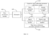
- the TISAR ADC includes an analog-to-digital conversion module 300, reference analog-to-digital convertor module 100, a calibration parameter calculation module 400, a capacitor array error compensation module 500 and a time delay adjustment module 600.
- the analog-to-digital conversion module 300 includes a plurality of analog-to-digital conversion sub-modules 310.
- the plurality of analog-to-digital conversion sub-modules 310 are configured to perform time-interleaved sampling on an analog signal input into the TISAR ADC, and each of the analog-to-digital conversion sub-modules 310 is able to generate an output digital signal.
- the reference analog-to-digital convertor module 100 is configured to sample the analog signal to generate a reference digital signal.
- the calibration parameter calculation module 400 is configured to obtain, according to the reference digital signal generated by the reference analog-to-digital convertor module 100 and the output digital signals generated by the analog-to-digital conversion sub-modules 310, capacitor array calibration parameters of the analog-to-digital conversion sub-modules 310 and time delay calibration parameters of the analog-to-digital conversion sub-modules 310.
- the capacitor array error compensation module 500 includes a plurality of error compensation sub-modules 510.
- the number of the error compensation sub-modules 510 is the same as the number of the analog-to-digital conversion sub-modules 310.
- the error compensation sub-modules 510 are in one-to-one correspondence to the analog-to-digital conversion sub-modules 310.
- the capacitor array error compensation sub-modules 510 are configured to adjust capacitor arrays of the corresponding analog-to-digital conversion sub-modules 310 according to the capacitor array calibration parameters of the analog-to-digital conversion sub-modules 310.
- the time delay adjustment module 600 includes a plurality of analog delay line sub-modules.
- the number of the analog delay line sub-modules is the same as the number of analog-to-digital conversion sub-modules 310.
- the analog delay line sub-modules are in one-to-one correspondence to the analog-to-digital conversion sub-modules 310.
- the analog delay line sub-modules are configured to adjust time delays of the corresponding analog-to-digital conversion sub-modules 310 according to the time delay calibration parameters of the analog-to-digital conversion sub-modules 310.
- the capacitor array error compensation module 500 is specifically a CDAC, i.e., a capacitor-type digital-to-analog conversion structure.
- the reference analog-to-digital convertor module 100 by configuring the reference analog-to-digital convertor module 100, the reference digital signal generated by the reference analog-to-digital convertor module 100 is compared with the output digital signals generated by the analog-to-digital conversion sub-modules 310 of the TISAR ADC to obtain errors of the output digital signals of the analog-to-digital conversion sub-modules 310.
- the calibration parameter calculation module 400 calculates capacitor array calibration parameters of the analog-to-digital conversion sub-modules 310 by utilizing the errors, and the capacitor array error compensation module 500 calibrates the capacitor array errors of the analog-to-digital conversion sub-modules 310 by utilizing the capacitor array calibration parameters. Meanwhile, the calibration parameter calculation module 400 calculate time delay calibration parameters of the analog-to-digital conversion sub-modules 310, and the time delay adjustment module 600 calibrate the time delay errors of the analog-to-digital conversion sub-modules 310 by utilizing the time delay calibration parameters. Thus, the capacitor array errors and time errors in the TISAR ADC are jointly calibrated, and the mutual influence of capacitor array errors and time errors is reduced.
- the calibration parameter calculation module 400 calculates the capacitor array calibration parameters and time delay calibration parameters of the analog-to-digital conversion sub-modules 310, the errors of the output digital signals of the analog-to-digital conversion sub-modules 310 only needs to be calculated for one time, so that the consumption of calculation resources can be decreased and the hardware circuit of the TISAR ADC can also be simplified.
- the calibration parameter calculation module 400 includes a subtractor 420, a capacitor array calibration parameter calculation module 430 and a time delay calibration parameter calculation module 440.
- the subtractor 420 is configured to calculate differences between the numerical values of the output digital signals generated by the analog-to-digital conversion sub-modules 310 and the numerical value of the reference digital signal at the corresponding sampling moment, respectively.
- the capacitor array calibration parameter calculation module 430 is configured to calculate, according to the differences calculated by the subtractor 420, capacitor array calibration parameters of the analog-to-digital conversion sub-modules 310, respectively.
- the time delay calibration parameter calculation module 440 is configured to calculate, according to the differences calculated by the subtractor 420, time delay calibration parameters of the analog-to-digital conversion sub-modules 310, respectively.
- the capacitor array calibration parameter calculation module 430 includes an error estimation module 431 and a weight calculation module 432.
- the error estimation module 431 is configured to calculate, according to the differences calculated by the subtractor 420, weight errors of capacitor arrays of the analog-to-digital conversion sub-modules 310, respectively.
- the weight calculation module 432 is configured to calculate, according to the weight errors calculated by the error estimation module 431, calibration weights of capacitor arrays of the corresponding analog-to-digital conversion sub-modules 310, and use the calibration weights as capacitor array calibration parameters of the analog-to-digital conversion sub-modules 310.
- the time delay parameter calculation module 440 includes a square summation module 441 and a digital control code calculate module 442.
- the square summation module 441 is configured to calculate the sum of squares of the differences corresponding to different sampling moments of each of the analog-to-digital conversion sub-modules 310.
- the digital control code calculate module 442 is configured to, for each of the analog-to-digital conversion sub-modules 310, calculate, according to the sum of squares calculated by the square summation module, a corresponding analog delay line digital control code of the analog-to-digital conversion sub-module 310, and use the analog delay line digital control code as a time delay calibration parameter of the analog-to-digital conversion sub-module 310.
- the TISAR ADC further includes a temperature sensor.
- the temperature sensor is configured to detect the temperature of the TISAR ADC and generate a temperature signal.
- the reference analog-to-digital convertor module 100 is configured to receive the temperature signal generated by the temperature signal and configured to, in the case that the temperature acquired in a predetermined time exceeds a predetermined range, sample the analog signal input into the TISAR ADC to generate the reference digital signal.
- the calibration parameter calculation module 400 is configured to determine whether the differences between the reference digital signal generated by the reference analog-to-digital converter module 100 and the output digital signals of the TISAR ADC are greater than a first threshold, and configured to, in the case that the differences between the reference digital signal and the output digital signals of the TISAR ADC are greater than the first threshold, obtain capacitor array calibration parameters of the analog-to-digital conversion sub-modules 310 and time delay calibration parameters of the analog-to-digital conversion sub-modules 310 according to the reference digital signal and the output digital signals generated by the analog-to-digital conversion sub-modules 310 of the TISAR ADC.
- the calibration parameter calculation module 400 is configured to determine whether the differences between the reference digital signal generated by the reference analog-to-digital converter module and the output digital signals of the TISAR ADC are less than a second threshold, and configured to, in the case that the differences between the reference digital signal and the output digital signals of the TISAR ADC are less than the second threshold, stop obtaining capacitor array calibration parameters of the analog-to-digital conversion sub-modules 310 and time delay calibration parameters of the analog-to-digital conversion sub-modules 310 according to the reference digital signal and the output digital signals generated by the analog-to-digital conversion sub-modules 310 of the TISAR ADC.
- the TISAR ADC includes a counting module.
- the counting module is configured to acquire the number of iterations of adjusting, by the capacitor array error compensation module, capacitor arrays of the corresponding analog-to-digital conversion sub-modules according to the capacitor array calibration parameters of the analog-to-digital conversion sub-modules respectively and adjusting, by the time delay adjustment module, time delays of the corresponding analog-to-digital conversion sub-modules according to the time delay calibration parameters of the analog-to-digital conversion sub-modules respectively.
- the reference analog-to-digital converter module 100 is configured to, in the case that the number of iterations exceeds a predetermined threshold, stop sampling the analog signal input into the TISAR ADC.
- the errors of the output digital signals of the analog-to-digital conversion sub-modules are obtained by comparing the reference digital signal with the output digital signals generated by the analog-to-digital conversion sub-modules of the TISAR ADC.
- the capacitor array calibration parameters of the analog-to-digital conversion sub-modules are calculated for calibrating the capacitor array errors of the TISAR ADC
- the time delay calibration parameters of the analog-to-digital conversion sub-modules are calculated for calibrating the time errors of the TISAR ADC. Accordingly, the capacitor array errors and time errors in the TISAR ADC are jointly calibrated, and the mutual influence of capacitor array errors and time errors is reduced.
- the errors of the output digital signals of the analog-to-digital conversion sub-modules do not need to be calculated repeatedly, so that the consumption of calculation resources can be decreased and the design requirement for the hardware circuit of the TISAR ADC can be reduced.
Landscapes
- Engineering & Computer Science (AREA)
- Theoretical Computer Science (AREA)
- Physics & Mathematics (AREA)
- Nonlinear Science (AREA)
- Analogue/Digital Conversion (AREA)
Applications Claiming Priority (2)
| Application Number | Priority Date | Filing Date | Title |
|---|---|---|---|
| CN201911249886.2A CN113037283B (zh) | 2019-12-09 | 2019-12-09 | 时间交织逐次逼近型模数转换器及其校准方法 |
| PCT/CN2020/124982 WO2021114939A1 (fr) | 2019-12-09 | 2020-10-29 | Convertisseur analogique-numérique à approximations successives à entrelacement temporel et son procédé d'étalonnage |
Publications (2)
| Publication Number | Publication Date |
|---|---|
| EP4072021A1 true EP4072021A1 (fr) | 2022-10-12 |
| EP4072021A4 EP4072021A4 (fr) | 2023-01-25 |
Family
ID=76328847
Family Applications (1)
| Application Number | Title | Priority Date | Filing Date |
|---|---|---|---|
| EP20898826.1A Pending EP4072021A4 (fr) | 2019-12-09 | 2020-10-29 | Convertisseur analogique-numérique à approximations successives à entrelacement temporel et son procédé d'étalonnage |
Country Status (4)
| Country | Link |
|---|---|
| US (1) | US12040810B2 (fr) |
| EP (1) | EP4072021A4 (fr) |
| CN (1) | CN113037283B (fr) |
| WO (1) | WO2021114939A1 (fr) |
Families Citing this family (11)
| Publication number | Priority date | Publication date | Assignee | Title |
|---|---|---|---|---|
| CN113805042B (zh) * | 2021-09-17 | 2022-10-18 | 普源精电科技股份有限公司 | 时延测量装置及测试方法 |
| KR102610407B1 (ko) * | 2021-10-01 | 2023-12-05 | 금오공과대학교 산학협력단 | 직렬 시간 인터리브 구조기반의 고성능 아날로그 디지털 컨버터 |
| CN114039603A (zh) * | 2021-11-09 | 2022-02-11 | 华南理工大学 | 一种双通道逐次逼近型模数转换器及其再开关方法 |
| CN115801005A (zh) * | 2022-11-16 | 2023-03-14 | 上海后摩智能科技有限公司 | 模数转换校准电路、多路模数转换电路、芯片及计算装置 |
| CN115664418B (zh) * | 2022-12-28 | 2023-02-28 | 江苏润石科技有限公司 | 基于非线性误差的sar adc的精度校准方法及装置 |
| CN116405033A (zh) * | 2023-03-10 | 2023-07-07 | 电子科技大学 | 一种高精度sar型模数转换器的前台校准方法 |
| CN115987287B (zh) * | 2023-03-20 | 2023-06-30 | 芯翼信息科技(南京)有限公司 | 基于模数转换器的参数校准方法及装置 |
| CN117254811A (zh) * | 2023-11-14 | 2023-12-19 | 北京智联安科技有限公司 | 逐次逼近型模数转换器及其电容阵列的校准方法和介质 |
| CN117555212B (zh) * | 2024-01-11 | 2024-04-09 | 深圳市山海半导体科技有限公司 | 延时模块、时间数字转换器、系统及方法 |
| CN119010905B (zh) * | 2024-08-16 | 2025-05-09 | 成都玖锦科技有限公司 | 一种时间交织采样电路实时校准方法、装置和系统 |
| CN119519709B (zh) * | 2024-10-29 | 2026-01-23 | 西安电子科技大学 | 基于分块LMS校准型高精度多级Pipelined_SAR ADC |
Family Cites Families (18)
| Publication number | Priority date | Publication date | Assignee | Title |
|---|---|---|---|---|
| US7219037B2 (en) * | 2002-10-24 | 2007-05-15 | Lecroy Corporation | High bandwidth oscilloscope |
| DE102004009612B4 (de) * | 2004-02-27 | 2010-11-18 | Infineon Technologies Ag | Verfahren und Schaltungsanordnung zum Verzögerungsabgleich von zeitversetzt arbeitenden Analog-Digital-Wandlern |
| US7408495B2 (en) * | 2006-05-15 | 2008-08-05 | Guzik Technical Enterprises | Digital equalization of multiple interleaved analog-to-digital converters |
| US20130344400A1 (en) * | 2010-12-07 | 2013-12-26 | Oregon State University | Biochemical systems for sulfur and carbon sequestration |
| US8519875B2 (en) * | 2011-04-12 | 2013-08-27 | Maxim Integrated Products, Inc. | System and method for background calibration of time interleaved analog to digital converters |
| US8471751B2 (en) * | 2011-06-30 | 2013-06-25 | Intel Corporation | Two-stage analog-to-digital converter using SAR and TDC |
| JP5537527B2 (ja) * | 2011-09-26 | 2014-07-02 | 株式会社東芝 | 時間誤差推定装置、誤差補正装置およびa/d変換器 |
| FR2982101A1 (fr) * | 2011-11-02 | 2013-05-03 | St Microelectronics Grenoble 2 | Etalonnage d'un adc entrelace |
| US9337853B2 (en) * | 2012-09-07 | 2016-05-10 | Hitachi, Ltd. | Interleaved A/D converter |
| WO2015120315A1 (fr) * | 2014-02-06 | 2015-08-13 | Massachusetts Institute Of Technology | Réduction d'erreurs de désalignement temporel dans des convertisseurs analogique-numérique à entrelacement temporel |
| US9287889B2 (en) * | 2014-04-17 | 2016-03-15 | The Board Of Regents, The University Of Texas System | System and method for dynamic path-mismatch equalization in time-interleaved ADC |
| WO2016003432A1 (fr) * | 2014-06-30 | 2016-01-07 | Synopsys, Inc. | Convertisseur analogique-numérique entrelacé et procédé d'étalonnage d'un convertisseur analogique-numérique entrelacé |
| US9401726B2 (en) * | 2014-11-26 | 2016-07-26 | Silicon Laboratories Inc. | Background calibration of time-interleaved analog-to-digital converters |
| US20170117914A1 (en) * | 2015-10-23 | 2017-04-27 | Industry-Academic Cooperation Foundation, Chosun University | Method and apparatus for providing digital background calibration for mismatches in m-channel time-interleved adcs (ti-adcs) |
| WO2019098981A1 (fr) | 2017-11-16 | 2019-05-23 | Sabanci Universitesi | Logique de sar à auto-détermination déclenchée par événement de can de sar asynchrones |
| CN108471313B (zh) | 2018-03-12 | 2021-07-02 | 东南大学 | 一种基于数模混合信号的tiadc系统校准方法 |
| CN109361392B (zh) | 2018-12-13 | 2022-05-03 | 江苏芯云电子科技有限公司 | 逐次逼近型模数转换器及其权重校准方法 |
| CN109861691B (zh) * | 2019-01-02 | 2020-08-28 | 西安电子科技大学 | 基于延迟锁相环的两步式混合结构sar tdc的模数转换器电路 |
-
2019
- 2019-12-09 CN CN201911249886.2A patent/CN113037283B/zh active Active
-
2020
- 2020-10-29 US US17/781,521 patent/US12040810B2/en active Active
- 2020-10-29 WO PCT/CN2020/124982 patent/WO2021114939A1/fr not_active Ceased
- 2020-10-29 EP EP20898826.1A patent/EP4072021A4/fr active Pending
Also Published As
| Publication number | Publication date |
|---|---|
| US12040810B2 (en) | 2024-07-16 |
| CN113037283B (zh) | 2025-12-26 |
| US20230047734A1 (en) | 2023-02-16 |
| EP4072021A4 (fr) | 2023-01-25 |
| CN113037283A (zh) | 2021-06-25 |
| WO2021114939A1 (fr) | 2021-06-17 |
Similar Documents
| Publication | Publication Date | Title |
|---|---|---|
| EP4072021A1 (fr) | Convertisseur analogique-numérique à approximations successives à entrelacement temporel et son procédé d'étalonnage | |
| US10291245B2 (en) | Device and method for correcting error estimation of analog-to-digital converter | |
| US8519875B2 (en) | System and method for background calibration of time interleaved analog to digital converters | |
| US11387838B1 (en) | SAR analog-to-digital converter calibration | |
| US10784882B2 (en) | Analog to digital converter device and method of calibrating clock skew | |
| CN102006073B (zh) | 一种快速收敛多通道时间交织模数转换器及其校准系统 | |
| US20140368364A1 (en) | Method and apparatus for estimating sampling delay error between first and second analog-to-digital converters of time-interleaved analog-to-digital converter | |
| US8174423B2 (en) | Pipelined analog-to-digital converter and sub-converter stage | |
| CN108432140B (zh) | 一种校正装置和方法 | |
| KR20180122367A (ko) | 교대 비교기를 갖는 adc의 dc 오프셋 보정 | |
| EP3565122A1 (fr) | Techniques d'amélioration de précision pour convertisseurs analogiques-numériques | |
| US8842029B2 (en) | Area-efficiency delta modulator for quantizing an analog signal | |
| US9866232B2 (en) | Analog-to-digital converter, radiation detector and wireless receiver | |
| CN105141312B (zh) | 一种n通道时域交织模数转换器时钟偏差的数字后台校准算法 | |
| US9685970B1 (en) | Analog-to-digital converting system and converting method | |
| CN108055039B (zh) | 一种用于tiadc采样时间误差的全数字校准模块及其校准方法 | |
| US10498349B2 (en) | Bit error rate forecast circuit for successive approximation register analog-to-digital conversion | |
| US8730083B2 (en) | Analog-digital converter with calibration and receiver including the converter | |
| CN112067868A (zh) | 一种具有自动校准功能的数字示波器多路adc交叉采样电路及其校准方法 | |
| US9831886B2 (en) | Background calibration for digital-to-analog converters | |
| US10644713B1 (en) | Process, voltage and temperature optimized asynchronous SAR ADC | |
| CN114448441A (zh) | 一种时钟校准方法、装置和设备 | |
| CN108832927B (zh) | 一种tiadc自校准系统 | |
| Song et al. | A 10-b 800MS/s time-interleaved SAR ADC with fast timing-skew calibration | |
| Liu et al. | 24.4 A 10b 3GS/s time-domain ADC with mutually exclusive metastability correction and wide common-mode input |
Legal Events
| Date | Code | Title | Description |
|---|---|---|---|
| STAA | Information on the status of an ep patent application or granted ep patent |
Free format text: STATUS: THE INTERNATIONAL PUBLICATION HAS BEEN MADE |
|
| PUAI | Public reference made under article 153(3) epc to a published international application that has entered the european phase |
Free format text: ORIGINAL CODE: 0009012 |
|
| STAA | Information on the status of an ep patent application or granted ep patent |
Free format text: STATUS: REQUEST FOR EXAMINATION WAS MADE |
|
| 17P | Request for examination filed |
Effective date: 20220706 |
|
| AK | Designated contracting states |
Kind code of ref document: A1 Designated state(s): AL AT BE BG CH CY CZ DE DK EE ES FI FR GB GR HR HU IE IS IT LI LT LU LV MC MK MT NL NO PL PT RO RS SE SI SK SM TR |
|
| A4 | Supplementary search report drawn up and despatched |
Effective date: 20230103 |
|
| RIC1 | Information provided on ipc code assigned before grant |
Ipc: H03M 1/08 20060101ALN20221221BHEP Ipc: H03M 1/46 20060101ALI20221221BHEP Ipc: H03M 1/12 20060101ALI20221221BHEP Ipc: H03M 1/10 20060101AFI20221221BHEP |
|
| DAV | Request for validation of the european patent (deleted) | ||
| DAX | Request for extension of the european patent (deleted) | ||
| STAA | Information on the status of an ep patent application or granted ep patent |
Free format text: STATUS: EXAMINATION IS IN PROGRESS |
|
| 17Q | First examination report despatched |
Effective date: 20241106 |